EP0303410B1 - Nichtlineare Squelch-Schaltung - Google Patents
Nichtlineare Squelch-Schaltung Download PDFInfo
- Publication number
- EP0303410B1 EP0303410B1 EP88307253A EP88307253A EP0303410B1 EP 0303410 B1 EP0303410 B1 EP 0303410B1 EP 88307253 A EP88307253 A EP 88307253A EP 88307253 A EP88307253 A EP 88307253A EP 0303410 B1 EP0303410 B1 EP 0303410B1
- Authority
- EP
- European Patent Office
- Prior art keywords
- signal
- level
- filtered
- signals
- squelch
- Prior art date
- Legal status (The legal status is an assumption and is not a legal conclusion. Google has not performed a legal analysis and makes no representation as to the accuracy of the status listed.)
- Expired - Lifetime
Links
- 239000003990 capacitor Substances 0.000 claims description 18
- 238000001914 filtration Methods 0.000 claims description 7
- 238000000034 method Methods 0.000 claims 4
- 238000001514 detection method Methods 0.000 claims 3
- 230000002459 sustained effect Effects 0.000 claims 1
- 230000004913 activation Effects 0.000 description 8
- 230000001052 transient effect Effects 0.000 description 5
- 230000007704 transition Effects 0.000 description 4
- 238000004804 winding Methods 0.000 description 4
- 230000001629 suppression Effects 0.000 description 3
- 230000033228 biological regulation Effects 0.000 description 2
- 238000010586 diagram Methods 0.000 description 2
- 230000003213 activating effect Effects 0.000 description 1
- 230000005540 biological transmission Effects 0.000 description 1
- 230000001351 cycling effect Effects 0.000 description 1
- 238000013479 data entry Methods 0.000 description 1
- 230000009849 deactivation Effects 0.000 description 1
- 230000007423 decrease Effects 0.000 description 1
- 230000000694 effects Effects 0.000 description 1
- 238000009434 installation Methods 0.000 description 1
- 230000004044 response Effects 0.000 description 1
- 230000000630 rising effect Effects 0.000 description 1
- 230000008054 signal transmission Effects 0.000 description 1
- 238000001228 spectrum Methods 0.000 description 1
Images

Classifications
-
- H—ELECTRICITY
- H04—ELECTRIC COMMUNICATION TECHNIQUE
- H04L—TRANSMISSION OF DIGITAL INFORMATION, e.g. TELEGRAPHIC COMMUNICATION
- H04L1/00—Arrangements for detecting or preventing errors in the information received
- H04L1/20—Arrangements for detecting or preventing errors in the information received using signal quality detector
Definitions
- This invention relates to interconnection of electronic equipment in a local area network and, more particularly, to a filtering and squelch circuit which eliminates impulse and other low frequency noise from falsely activating equipment located on the network.
- Shielded coax cable allows interconnection in a local area network (LAN) covering up to 300 linear feet distance. This is because external radio frequency (RF) energy is not induced in shielded coax cable and because crosstalk energy between parallel cables is suppressed by the use of such cable.
- LAN local area network
- RF radio frequency
- TP twisted-pair
- unshielded wires to interconnect electronic equipment, such as computers, workstations, data entry terminals, and the like.
- TP twisted-pair
- TP wires act as an antenna and are susceptible to external radio frequency (RF) energy.
- RF radio frequency
- This RF noise can swamp a signal carried by the TP wires and thus they provide very poor signal-to-noise (S/N) ratios.
- S/N signal-to-noise
- S/N ratios can be improved by using very high signal transmission power levels, but FCC regulations specify maximum tansmission levels and high power tansmission is costly.
- a better solution is to provide a totally differential balanced receiver and to filter at transmission to fall within the FCC regulations, and filter at receiver to 40-100 megahertz (MHz) which then eliminates bulk of external RF noise susceptibility.
- EP-A-0 132 307 discloses a non-linear filter comprising: filter means responsive to a received signal for generating filtered differential signals representing said received signals having a frequency between a first and a second predetermined frequency; squelch means responsive to said filtered signals for generating a squelch signal at a first level when a noise pulse is detected in the filtered signal and at a second level when no noise pulse is detected, and logic means responsive to said filtered signals and said squelch signal for suppressing said filtered signals upon reception of said first level of said squelch signal and for not suppressing said filtered signals upon reception of said second level of said squelch signal.
- filter means responsive to a received signal for generating filtered differential signals representing said received signals having a frequency between a first and a second predetermined frequency
- squelch means responsive to said filtered signals for generating a squelch signal at a first level when a noise pulse is detected in the filtered signal and at a second level when no noise pulse is detected
- a non-linear filter comprising: filter means responsive to a received signal for generating filtered differential signals representing said received signals having a frequency between a first and a second predetermined frequency; squelch means reponsive to said filtered signals for generating a squelch signal at a first level when a noise pulse is detected in the filtered signal and at a second level when no noise pulse is detected, and logic means responsive to said filtered signals and said squelch signal for suppressing said filtered signals upon reception of said first level of said squelch signal and for not suppressing said filtered signals upon reception of said second level of said squelch signal, characterized in that the squelch signal at said first level is generated upon reception of no more than a predetermined number of consecutive half-cycles of said filtered signals within a preselected frequency range and within a preselected amplitude range, and at said second level upon reception of more than said predetermined number of consecutive half-cycles of said filtered signals within said
- a low-cost filter and non-linear squelch circuit is provided by the present invention which, employed in a receiver in a LAN, eliminates low frequency noise and impulses present by virtue of un-shielded TP wires interconnecting elements on the LAN.
- the low pass filter and non-linear squelch circuit assures that only signals having the right frequency - 3 MHz to 15 MHz in the case of the IEEE 802.3 standards - and which are not transient impulses, will be passed to the receiver, causing its activation.
- the resulting non-linear filter provides an inexpensive (approximately 50 cents) solution to the attenuation of error-causing transient "spikes" in the LAN and employs emitter-coupled logic (ECL) circuitry for speed.
- ECL emitter-coupled logic
- the invention assures that only a multiple transition of at least three half-cycles of a received waveform, at a proper frequency, each half-cycle exceeding a threshold level will activate the receiver. While a single half-cycle, although at a proper frequency and exceeding the threshold will not falsely activate the receiver. Employing certain circuit values, even a double half-cycle will not falsely activate the receiver.
- the non-linear squelch portion of the circuit employs ECL comparators and logic elements providing fast suppression of transient impulses so as to avoid false activation of the receiver.
- Each of a pair of ECL comparators receive the positive or negative portion of the filtered differential signal generated by the low pass filter.
- a threshold value is also supplied to each comparator and a signal is generated by each comparator if the filtered signal it receives exceeds the threshold.
- An RC circuit is connected to the output terminal of each comparator to provide a time constant for the decay of the signal generated by the comparator. This time constant is chosen to cut off all frequencies lower than 3 MHz.
- An ECL NAND gate receives the signals generated by the comparator.
- a second RC circuit is connected to the output terminal of the NAND gate to avoid double-cycle false activation.
- a final ECL comparator generates a squelch signal at a level appropriate for suppressing signals generated by the low-pass filter.
- Fig.1 is a logic diagram of the non-linear squelch circuit of the instant invention.
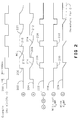
- Fig.2 is a waveform diagram illustrating the operation of the squelch circuit of the instant invention.
- a pair of terminals 50 and 52 carries the signals received on one TP wire by a transceiver. These wires comprise one-half of the full-duplex interconnection commonly employed in telephone equipment.
- the signals carried thereon follow IEEE 802.3 LAN standard Protocol.
- a transformer 54 receives at its primary winding the signals present at terminals 50 and 52.
- a secondary winding of transformer 54 generates signals to the low-pass filter (LPF) 56 of the present invention.
- LPF low-pass filter
- LPF 56 includes resistors 58 and 60 connected in series between the secondary windings of transformer 54.
- a first terminal of a capacitor 62 is connected to the common point of the resistors 58 and 60.
- the second terminal of capacitor 62 is connected to ground.
- a pair of resistors 64 and 66 have a first terminal connected to each end of the secondary windings of transformer 54.
- the second terminals of resistors 64 and 66 are connected to a first terminal of inductors 68 and 70, respectively.
- a capacitor 72 is connected between the second terminals of resistors 64 and 66.
- a capacitor 74 is connected between the second terminals of inductors 68 and 70.
- inductors 68 and 70 Also connected between the second terminals of inductors 68 and 70 is a series connection of resistors 76 and 78.
- the second terminals of inductors 68 and 70 is also connected to an inverting and a non-inverting input, respectively, of an amplifier (amp) 82.
- the common point of resistors 76 and 78 receives a reference voltage generated by a voltage source 83.
- the signals generated by amp 82 are differential signals passed by the low pass filter section 56 of the instant invention.
- Squelch portion includes ECL comparators 86 and 88 receiving at a non-inverting and an invorting terminal, respectively, the differential signals generated by amp 82. Inverting and non-inverting terminal, respectively, of comparators 86 and 88 are connected to the common point of a series connection of resistors 90 and 92. The resistors 90 and 92 serve as a voltage-divider and are connected between the reference voltage source 83 and ground.
- comparators 86 and 88 are connected to the inputs of an ECL AND gate 94.
- a capacitor 96 and a resistor 98 are connected between the output terminal of comparator 86 and ground.
- a capacitor 100 and a resistor 102 are connected between the output terminal of comparator 88 and ground.
- a complementing output terminal of AND gate 94 is connected to an inverting input of an ECL comparator 104. Accordingly, AND gate 94 functions as a NAND gate, and will be referred to thusly hereinafter.
- a capacitor 106 and a resistor 108 are connected between the output terminal of NAND gate 94 and ground.
- a voltage source 110 is connected to a non-inverting input of comparator 104.
- the signal generated by comparator 104 is a squelch generated by squelch portion 84 of non-linear squelch circuit of the instant invention.
- the voltage generated by voltage source 84 as divided by resistors 90 and 92 provides a reference voltage so that the squelch signal generated by comparator 104 has a predetermined threshold value.
- a resistor 111 is connected between the output terminal of comparator 104 and the common point of connection of resistors 90 and 92. Resistor 111 provides a hysteresis effect which avoids off-on-off-on cycling of the squelch circuit at the threshold.
- the signals generated by amp 82 are also conducted to an inverting and a non-inverting input terminal of an amplifier 112.
- the input terminals of amp 112 are connected to ground via resistors 114 and 116, respectively.
- the signals generated by op amp 112 are differential signals conducted to a first input terminal of ECL AND gate 118 and 120, respectively.
- Second input terminals of gates 118 and 120 receive the squelch signal generated by comparator 104.
- the first input terminals of AND gates 118 and 120 are connected to ground via resistors 122 and 124, respectively.
- Signals generated at the output terminals of AND gates 118 and 120 represent the differential signals actually applied to data terminal equipment connected to the LAN via the Pod including the receiver section including low-pass filter 56 and the squelch 84, comprising the non-linear squelch circuit of the instant invention.
- LPF 56 acts a linear differential-mode rejection filter preferably having flat response at 3 MHz and a 3 dB attenuation at 15 MHz.
- Common-mode rejection is provided by transformer 54, and LPF56.
- a pod and Hub connected via twisted-paid unshielded wires in a LAN are sensitive to signals in the frequency range 3-15 MHz in accordance with the IEEE 802.3 LAN 10 base 5 standard power spectrum.
- LPF 56 attenuates much of the impulse and high-frequency noise associated with the use of unshielded TP wires.
- spurious transient signals representing high-frequency impulse noise or large low-frequency crosstalk noise in the LAN may falsely activate the DTE connected to the LAN because the LPF 56 will pass such noise if it is in the bandpass frequency 50KHz - 15MHz.
- Squelch circuit 84 receives differential signals Rx+ and Rx- generated by amp 82 of LPF 56, as shown as waveform 200 of Fig. 2. Because of the application of Rx+ and Rx- to inverting and non-inverting terminals of comparators 86 and 88, respectively, the difference (Rx+) - (Rx-) signal is depicted as waveform 200. The signals generated by comparators 88 and 86 are shown as waveforms 202 and 204, respectively.
- Each waveform experiences a sharp rise 206, 208, 210 and 212 at successive transitions of waveform 200 and a smooth drop 214, 216, 218 and 220 determined by the RC time constant determined by the values of resistor-capacitor combination 98 and 96, and 102 and 100 connected to the output terminal of comparator 86 and 88, respectively.
- the magnitude of the rise and overall drop shown for waveforms 202 and 204 is determined by a reference voltage generated by voltage source 83 and voltage divider comprising resistors 90 and 92.
- the logical product of waveforms 202 and 204 is generated by NAND gate 94 and is shown as waveform 222. As shown, it comprises a signal reaching a HIGH level 224 and 226 upon every rising transition of waveform 200.
- capacitor 106 is omitted, and a corresponding waveform 228 is generated by comprator 104 representing the squelch signal applied to AND gates 118 and 120.
- a single one-half cycle transition of waveform 200 will accordingly cause waveform 228 to produce a LOW logic level signal such as shown at 230 and 232 in Fig. 2.
- AND gates 118 and 120 will not pass the differential signal passed by LPF 56 as generated by amp 112.
- a single positive-going impulse even within the 3-15 MHz bandpass frequency of LPF 56 will be suppressed. Accordingly, false activation of the DTE connected to the LAN via a Pod including the non-linear squelch circuit of the instant invention, will be avoided.
- NAND gate 94 Two or more pulses occurring close in time, then, will result in NAND gate 94 generating at its complemented output, a logic LOW coincident with the second pulse.
- This LOW will be applied to the inverting terminal of comparator 104 which will, in turn, generate a logic HIGH signal.
- This signal when applied to AND gates 118 and 120 will not suppress the differential signals passed by LPF 56 and these differential signals will be applied to the DTE and will correctly activate it.
- capacitor 106 In the embodiment without capacitor 106, multiple low-frequency half-cycles of noise less than 3MHz will produce undesirable false deactivation and activation of the squelch circuit.
- consecutive double half-cycles, representing one complete cycle of a spurious transient impulse can be suppresed so as to avoid false activation of the DTE equipment connected to the LAN via the Pod.
- capacitor 106 is included in the squelch circuit 84. The value for capacitor 106 is selected so that even though two consecutive impulses cause AND gate 94 to generate the LOW logic signal as described hereinabove, the signal so-generated decay as shown in waveform 234 of Fig. 2.
- capacitor 106 will however be chosen so that three or more consecutive half-wave pulses will occur over a sufficiently long time to assure ample decay of the waveform 234 to permit generation by comparator 104 of a HIGH logic level. This, in turn, places AND gates 118 and 120 in an "ON" mode thereby permitting passage of received signals to the DTE.
- the elements 86, 88, 94 and 104 of squelch circuit 84 are preferably ECL monolithic circuits which afford speed to permit fast suppression of impulse noise. Yet, because of the simplicity of the squelch circuit of the present invention, it provides a non-linear filter function at low cost. In another embodiment of the invention, open collector transistor-tansistor logic (TTL) circuitry could be employed to provide the requisite speed.
- TTL transistor-tansistor logic
Landscapes
- Engineering & Computer Science (AREA)
- Quality & Reliability (AREA)
- Computer Networks & Wireless Communication (AREA)
- Signal Processing (AREA)
- Noise Elimination (AREA)
- Networks Using Active Elements (AREA)
- Dc Digital Transmission (AREA)
Claims (12)
- Nichtlineares Filter, mit einer Filtervorrichtung (56), die auf ein empfangenes Signal anspricht, um gefilterte Differentialsignale zu erzeugen, welche das empfangene Signal darstellen und eine Frequenz zwischen einer ersten und einer Zweiten vorgegebenen Frequenz haben; einer Squelch-Vorrichtung (84), die auf die gefilterten Signale anspricht, um ein Squelch-Signal bei einem ersten Pegel zu erzeugen, wenn ein Störimpuls in dem gefilterten Signal erfaßt wird, und bei einem zweiten Pegel, wenn kein Störimpuls erfaßt wird; und einer Logikvorrichtung (118, 120), die auf die gefilterten Signale und das Squelch-Signal anspricht, um die gefilterten Signale beim Empfang des ersten Pegels des Squelch-Signales Zu unterdrücken und um die gefilterten Signale bei Empfang des zweiten Pegels des Squelch-Signales nicht zu unterdrücken, dadurch gekennzeichnet, daß das Squelch-Signal bei Empfang von nicht mehr als einer vorgegebenen Anzahl von aufeinanderfolgenden Halbzyklen der gefilterten Signale innerhalb eines voreingestellten Frequenzbereiches und innerhalb eines voreingestellten Amplitudenbereiches bei dem ersten Pegel erzeugt wird und bei Empfang von mehr als der vorgegebenen Anzahl aufeinanderfolgender Halbzyklen des gefilterten Signales innerhalb des voreingestellten Frequenzbereiches und des voreingestellten Amplitudenbereiches bei dem Zweiten Pegel erzeugt wird.
- Nichtlineares Filter nach Anspruch 1, mit weiterhin einer Vorrichtung (83) zum Erzeugen einer ersten Bezugsspannung, wobei die Squelch-Vorrichtung (84) umfaßt: eine erste Vergleichervorrichtung (86), die auf ein erstes der gefilterten Differentialsignaie und die erste Bezugsspannung anspricht, um bei einem Ausgang ein binärwertiges Signal zu erzeugen, das angibt, ob das erste gefilterte Differentialsignal die erste Bezugsspannung überschreitet; eine zweite Vergleichervorrichtung (88), die auf ein zweites der gefilterten Differentialsignale und die erste Bezugsspannung anspricht, um bei einem Ausgang ein binärwärtiges Signal zu erzeugen, das angibt, ob die erste Bezugsspannung das zweite gefilterte Differentialsignal überschreitet; eine erste und eine zweite Passiv-Vorrichtung (96, 98, 100, 102), die mit den Ausgängen der ersten bzw. der zweiten Vergleichervorrichtung verbunden ist, um den Zeitpunkt, zu dem das von der ersten bzw. der zweiten Vergleichervorrichtung erzeugte Signal sich von einem ersten binären Wert in einen zweiten binären Wert ändert, um einen ausgewählten Betrag zu verzögern; und eine Spitzenwert-Detektorvorrichtung (94, 110), die die bei den Ausgängen der ersten und der zweiten Vergleichervorrichtung erzeugten Signale empfängt, um bei einem Ausgang das zweipeglige Squelch-Signal zu erzeugen, wenn der Absolutwert beider empfangener Signale innerhalb der ersten ausgewählten Verzögerungszeit eine zweite vorgegebene Bezugsspannung überschreiten, und dadurch den Empfang von nicht mehr als der vorgegebenen Anzahl von aufeinanderfolgenden Halbzyklen des gefilterten Signales anzuzeigen.
- Nichtlineares Filter nach Anspruch 2, bei dem die Spitzenwert-Detektorvorrichtung aufweist: ein NAND-Gatter (94) mit einem ersten und einem zweiten Eingangsanschluß, die mit dem Ausgang der ersten bzw. der zweiten Vergleichervorrichtung (86, 88) verbunden sind und bei einem Ausgangsanschluß daraus ein Signal erzeugen; eine Vorrichtung (110) zum Erzeugen der zweiten vorgegebenen Bezugsspannung; und eine dritte Vergleichervorrichtung (104), die auf die zweite vorgegebene Bezugsspannung und auf das von dem NAND-Gatter erzeugte Signal anspricht, um bei einem Ausgang das zweipeglige Squelch-Signal zu erzeugen, das angibt, ob das von dem NAND-Gatter erzeugte Signal die zweite Bezugsspannung überschreitet, um so den Empfang von nur einem der aufeinanderfolgenden Halbzyklen des gefilterten Signals bei dem ersten Pegel oder von mindestens zweien der aufeinanderfolgenden Halbzyklen des gefilterten Signals bei dem ersten Pegel anzuzeigen.
- Nichtlineares Filter nach Anspruch 3, bei der die Spitzenwert-Detektorvorrichtung weiterhin aufweist: eine dritte Passiv-Vorrichtung (106, 108), die mit dem Ausgangsanschluß des NAND-Gatters (94) verbunden ist, um den Zeitpunkt, zu dem sich das am Ausgangsanschluß des NAND-Gatters erzeugte Signal von einem ersten zu einem zweiten Pegel verändert, um einen zweiten ausgewählten Wert zu verzögern, wobei das von der dritten Vergleichervorrichtung erzeugte Squelch-Signal den Empfang von nur zwei aufeinanderfolgenden Halbzyklen des gefilterten Signals beim ersten Pegel und von mindestens drei aufeinanderfolgenden Kalbzyklen des gefilterten Signals bei dem zweiten Pegel anzeigt.
- Nichtlineares Filter nach einem der vorangehenden Ansprüche, bei dem die Logikvorrichtung aufweist: ein erstes UND-Gatter (118), das bei einem ersten Eingang ein erstes der gefilterten Differentialsignale empfängt und bei einem zweiten Eingang das Squelch-Signal empfängt und bei einem Ausgangsanschluß ein erstes gefiltertes, unterdrücktes Differentialsignal erzeugt; und ein zweites UND-Gatter (120), das bei einem ersten Eingang ein zweites der gefilterten Differentialsignale und bei einem zweiten Eingang das Squelch-Signal empfängt und bei einem Ausgangsanschluß ein zweites gefiltertes, unterdrücktes Differentialsignal erzeugt.
- Nichtlineares Filter nach einen der Ansprüche 2 bis 5, bei dem die erste passive Verzögerungsvorrichtung einen ersten Kondensator (96) mit einer ersten Kapazität aufweist, der zwischen dem Ausgang der ersten Vergleichervorrichtung (86) und Masse angeschlossen ist, sowie einen ersten Widerstand (98) mit einem ersten Widerstandswert, der zwischen dem Ausgang der ersten Vergleichervorrichtung und Masse angeschlossen ist; bei dem die zweite passive Verzögerungsvorrichtung einen zweiten Kondensator (100) mit der ersten Kapazität aufweist, der zwischen dem Ausgang der zweiten Vergleichervorrichtung (98) und Masse angeschlossen ist, sowie einen zweiten Widerstand (102) mit dem ersten Widerstandswert, der zwischen dem Ausgang der zweiten Vergleichervorrichtung und Masse angeschlossen ist; und bei dem die erste ausgewählte Verzögerung die von der ersten Kapazität und dem ersten Widerstandswert vorgesehene RC-"Zeitkonstante" ist.
- Nichtlineares Filter nach einem der Ansprüche 4 bis 6, bei dem die dritte passive Verzögerungsvorrichtung einen dritten Kondensator (106) mit einer zweiten Kapazität aufweist, der zwischen dem Ausgangsanschluß des NAND-Gatters (94) und Masse angeschlossen ist, sowie einen dritten Widerstand (108) mit einem zweiten Widerstandswert, der zwischen dem Ausgangsanschluß des NAND-Gatters und Masse angeschlossen ist, wobei die zweite ausgewählte Verzögerung die von der zweiten Kapazität und dem zweiten Widerstand vorgesehene RC-"Zeitkonstante" ist.
- Nichtlineares Filter nach einem der Ansprüche 3 bis 7, bei dem die erste und die zweite Vergleichervorrichtung (86, 88) jeweils mindestens einen mit der ersten Bezugsspannung (83) verbundenen Eingangsanschluß aufweisen, wobei die ersten Eingangsanschlüsse miteinander verbunden sind, wobei das nichtlineare Filter (56) ferner eine Widerstandsvorrichtung (92) aufweist, die zwischen dem Ausgang der dritten Vergleichervorrichtung und der gemeinsamen Verbindung der ersten Eingangsanschlüsse der ersten und der zweiten Vergleichervorrichtung angeschlossen ist, um eine Hysterese innerhalb der Squelch-Vorrichtung (84) zu bewirken.
- Verfahren zum nichtlinearen Filtern eines empfangenen Signales, mit den Verfahrensschritten:a) Filtern des empfangenen Signales durch Dämpfung außerhalb eines vorgegebenen Frequenz-Durchlaßbereiches; undb) Erzeugen eines Squelch-Signales bei einem ersten Pegel beim Empfang von nicht mehr als einer vorgegebenen Anzahl von aufeinanderfolgenden Halbzyklen des gefilterten Signals innerhalb eines voreingestellten Frequenzbereiches und innerhalb eines voreingestellten Amplitudenbereiches und bei einem zweiten Pegel beim Empfang von mehr als der vorgegebenen Anzahl von aufeinanderfolgenden Halbzyklern des gefilterten Signales innerhalb des voreingestellten Frequenzbereiches und des voreingestellten Amplitudenbereiches; und Unterdrücken der gefilterten Signale beim Empfang des ersten Pegels des Squelch-Signales und nicht Unterdrücken der gefilterten Signale bei Empfang des Zweiten Pegels des Squelch-Signales.
- Nichtlineares Filterverfahren nach Anspruch 9, bei dem der Schritt (b) umfaßt:(b1) Vergleichen der gefilterten Signale mit einer ersten und einer zweiten vorgegebenen Bezugsspannung,(b2) Erzeugen eines ersten zweipegligen Signales bei einem ersten Pegel, wenn die gefilterten Signale die erste Bezugsspannung überschreiten, und Erzeugen eines zweiten zweipegligen Signales bei einem ersten Pegel, wenn die gefilterten Signale kleiner sind als die zweite Bezugsspannung,(b3) Verzögern des ersten und des zweiten Signales um einen ausgewählten Wert in der Zeit, zu der das erste und das zweite Signal von dem ersten Pegel auf einen Zweiten Pegel gehen,(b4) Erzeugen eines ersten Pegels eines zweipegiigen Squelch-Signales, wenn das erste und das Zweite Signal innerhalb der ausgewählten Verzögerungszeit eine dritte vorgegebene Bezugsspannung überschreiten, und(b5) Unterdrücken der gefilterten Signale beim Erzeugen des ersten Pegels des Squelch-Signales.
- Nichtlineares Filterverfahren nach Anspruch 10, bei dem der Schritt (b4) ferner das Verzögern des Erzeugens des Squelch-Signales um einen ausgewählten Wert in der Zeit umfaßt, zu der das Squelch-Signal von dem ersten Pegel auf einen zweiten Pegel geht.
- Nichtlineares Filterverfahren nach Anspruch 10 oder 11, bei dem die Verzögerung im Schritt (b3) so gewählt ist, daß die gefilterten Signale unterdrückt werden, wenn sie nicht mindestens einen Halbzyklus andauern.
Applications Claiming Priority (2)
| Application Number | Priority Date | Filing Date | Title |
|---|---|---|---|
| US07/084,961 US4908530A (en) | 1987-08-13 | 1987-08-13 | Non-linear squelch circuit for IEEE-802. 3 protocol |
| US84961 | 1987-08-13 |
Publications (3)
| Publication Number | Publication Date |
|---|---|
| EP0303410A2 EP0303410A2 (de) | 1989-02-15 |
| EP0303410A3 EP0303410A3 (en) | 1990-04-04 |
| EP0303410B1 true EP0303410B1 (de) | 1993-11-18 |
Family
ID=22188308
Family Applications (1)
| Application Number | Title | Priority Date | Filing Date |
|---|---|---|---|
| EP88307253A Expired - Lifetime EP0303410B1 (de) | 1987-08-13 | 1988-08-05 | Nichtlineare Squelch-Schaltung |
Country Status (5)
| Country | Link |
|---|---|
| US (1) | US4908530A (de) |
| EP (1) | EP0303410B1 (de) |
| JP (1) | JPS6471246A (de) |
| CA (1) | CA1321415C (de) |
| DE (1) | DE3885673T2 (de) |
Families Citing this family (10)
| Publication number | Priority date | Publication date | Assignee | Title |
|---|---|---|---|---|
| US5164960A (en) * | 1990-02-15 | 1992-11-17 | Advanced Micro Devices Inc. | Medium attachment unit for use with twisted pair local area network |
| US5191581A (en) * | 1990-12-07 | 1993-03-02 | Digital Equipment Corporation | Method and apparatus for providing high performance interconnection between interface circuits coupled to information buses |
| DE69221338T2 (de) * | 1991-01-18 | 1998-03-19 | Nat Semiconductor Corp | Steuervorrichtung für Wiederholerschnittstelle |
| US5412498A (en) * | 1991-03-29 | 1995-05-02 | Raynet Corporation | Multi-RC time constant receiver |
| US5418821A (en) * | 1991-10-15 | 1995-05-23 | National Semiconductor Corporation | Method and apparatus for sample-data receiver squelch |
| US5436934A (en) * | 1992-08-13 | 1995-07-25 | 3 Com Corporation | Differential high frequency level detector and data restoration circuit including squelch offset and slicing offset |
| US5550836A (en) * | 1992-11-06 | 1996-08-27 | Hewlett-Packard Company | High speed data transfer over twisted pair cabling |
| US5920203A (en) * | 1996-12-24 | 1999-07-06 | Lucent Technologies Inc. | Logic driven level shifter |
| US7120408B2 (en) * | 2003-07-31 | 2006-10-10 | Agilent Technologies, Inc. | Differential signal squelch detection circuit and method |
| DE102007048164B4 (de) * | 2007-10-08 | 2013-01-17 | Siemens Aktiengesellschaft | Verfahren zur kontaktlosen Übertragung wenigstens eines differentiellen Signals zwischen einem Sender und einem Empfänger bei Vorliegen wenigstens eines Gleichtaktstörsignals sowie zugehörige Schaltungsanordnung |
Family Cites Families (5)
| Publication number | Priority date | Publication date | Assignee | Title |
|---|---|---|---|---|
| DE3030866A1 (de) * | 1980-08-14 | 1982-03-11 | Siemens AG, 1000 Berlin und 8000 München | Verfahren und schaltungsanordnung zur unterdrueckung von stoerimpulsen |
| US4504959A (en) * | 1983-02-25 | 1985-03-12 | Johnson Service Company | Noise-neutralizing digital interface circuit |
| GB8317200D0 (en) * | 1983-06-24 | 1983-07-27 | Motorola Gmbh | Receiver having noise blanker |
| US4597082A (en) * | 1984-03-06 | 1986-06-24 | Controlonics Corporation | Transceiver for multi-drop local area networks |
| US4602364A (en) * | 1984-04-23 | 1986-07-22 | Codex Corporation | Local area data communication network |
-
1987
- 1987-08-13 US US07/084,961 patent/US4908530A/en not_active Expired - Fee Related
-
1988
- 1988-06-24 CA CA000570340A patent/CA1321415C/en not_active Expired - Fee Related
- 1988-08-05 DE DE3885673T patent/DE3885673T2/de not_active Expired - Fee Related
- 1988-08-05 EP EP88307253A patent/EP0303410B1/de not_active Expired - Lifetime
- 1988-08-10 JP JP63199751A patent/JPS6471246A/ja active Pending
Also Published As
| Publication number | Publication date |
|---|---|
| DE3885673D1 (de) | 1993-12-23 |
| EP0303410A3 (en) | 1990-04-04 |
| CA1321415C (en) | 1993-08-17 |
| DE3885673T2 (de) | 1994-05-26 |
| EP0303410A2 (de) | 1989-02-15 |
| JPS6471246A (en) | 1989-03-16 |
| US4908530A (en) | 1990-03-13 |
Similar Documents
| Publication | Publication Date | Title |
|---|---|---|
| JP2722213B2 (ja) | 整合装置 | |
| US6246718B1 (en) | Method and apparatus for decoding a bit sequence for transmission over pots wiring | |
| US6292517B1 (en) | Method and apparatus for detecting a data signal on a carrier medium | |
| US6771774B1 (en) | Filter arrangement for shaping a pulse propagated over pots wiring, and a method of manufacturing the same | |
| US5903605A (en) | Jitter detection method and apparatus | |
| US4908530A (en) | Non-linear squelch circuit for IEEE-802. 3 protocol | |
| JPH10511242A (ja) | 無線通信システム用の衝突検出装置および方法 | |
| US5493650A (en) | Apparatus and method for monitoring the presence of cables connected to ports of a computer network controller and automatically reconfiguring the network when cables are connected to or removed from the controller | |
| US5555277A (en) | Technique for cancelling common mode switching noise to achieve reduced error rates in a local area network | |
| US5161185A (en) | Method and apparatus for reducing noise in a digital voltage signal | |
| JPS6343444A (ja) | 多ノ−ド・バス・トポロジ−を有する局部区域ネットワ−ク | |
| US5315597A (en) | Method and means for automatically detecting and correcting a polarlity error in twisted-pair media | |
| US5418821A (en) | Method and apparatus for sample-data receiver squelch | |
| US6879645B1 (en) | Method and apparatus for dynamically varying the noise sensitivity of a receiver | |
| US4984248A (en) | High speed transceiver | |
| US5003556A (en) | Squelch circuit | |
| US4068174A (en) | Digital carrier wave detect circuitry | |
| EP0240245B1 (de) | Erkennen von Gleichstrom bei Vorhandensein von Datensignalen | |
| EP0281313B1 (de) | Digitale Empfangsfilterschaltung | |
| EP0008220A1 (de) | Schnittstelle für Zweifrequenz-Tondekodiersystem | |
| JPH01260949A (ja) | 衝突検出回路 | |
| EP0214159A1 (de) | Datenbus pilotton | |
| US4472816A (en) | FSK Discriminator | |
| JPS58131848A (ja) | デ−タバス衝突検出方式 | |
| US6879644B1 (en) | Method and apparatus for automatically determining a peak voltage level for a data signal propagated on a carrier medium |
Legal Events
| Date | Code | Title | Description |
|---|---|---|---|
| PUAI | Public reference made under article 153(3) epc to a published international application that has entered the european phase |
Free format text: ORIGINAL CODE: 0009012 |
|
| AK | Designated contracting states |
Kind code of ref document: A2 Designated state(s): DE FR GB IT |
|
| PUAL | Search report despatched |
Free format text: ORIGINAL CODE: 0009013 |
|
| AK | Designated contracting states |
Kind code of ref document: A3 Designated state(s): DE FR GB IT |
|
| 17P | Request for examination filed |
Effective date: 19900928 |
|
| 17Q | First examination report despatched |
Effective date: 19920708 |
|
| GRAA | (expected) grant |
Free format text: ORIGINAL CODE: 0009210 |
|
| AK | Designated contracting states |
Kind code of ref document: B1 Designated state(s): DE FR GB IT |
|
| REF | Corresponds to: |
Ref document number: 3885673 Country of ref document: DE Date of ref document: 19931223 |
|
| ET | Fr: translation filed | ||
| ITF | It: translation for a ep patent filed | ||
| PLBE | No opposition filed within time limit |
Free format text: ORIGINAL CODE: 0009261 |
|
| STAA | Information on the status of an ep patent application or granted ep patent |
Free format text: STATUS: NO OPPOSITION FILED WITHIN TIME LIMIT |
|
| 26N | No opposition filed | ||
| PGFP | Annual fee paid to national office [announced via postgrant information from national office to epo] |
Ref country code: FR Payment date: 19960715 Year of fee payment: 9 |
|
| PGFP | Annual fee paid to national office [announced via postgrant information from national office to epo] |
Ref country code: DE Payment date: 19960716 Year of fee payment: 9 |
|
| PGFP | Annual fee paid to national office [announced via postgrant information from national office to epo] |
Ref country code: GB Payment date: 19960724 Year of fee payment: 9 |
|
| PG25 | Lapsed in a contracting state [announced via postgrant information from national office to epo] |
Ref country code: GB Free format text: LAPSE BECAUSE OF NON-PAYMENT OF DUE FEES Effective date: 19970805 |
|
| GBPC | Gb: european patent ceased through non-payment of renewal fee |
Effective date: 19970805 |
|
| PG25 | Lapsed in a contracting state [announced via postgrant information from national office to epo] |
Ref country code: FR Free format text: LAPSE BECAUSE OF NON-PAYMENT OF DUE FEES Effective date: 19980430 |
|
| PG25 | Lapsed in a contracting state [announced via postgrant information from national office to epo] |
Ref country code: DE Free format text: LAPSE BECAUSE OF NON-PAYMENT OF DUE FEES Effective date: 19980501 |
|
| REG | Reference to a national code |
Ref country code: FR Ref legal event code: ST |
|
| PG25 | Lapsed in a contracting state [announced via postgrant information from national office to epo] |
Ref country code: IT Free format text: LAPSE BECAUSE OF NON-PAYMENT OF DUE FEES;WARNING: LAPSES OF ITALIAN PATENTS WITH EFFECTIVE DATE BEFORE 2007 MAY HAVE OCCURRED AT ANY TIME BEFORE 2007. THE CORRECT EFFECTIVE DATE MAY BE DIFFERENT FROM THE ONE RECORDED. Effective date: 20050805 |