EP0234212B1 - Electroplating cell - Google Patents
Electroplating cell Download PDFInfo
- Publication number
- EP0234212B1 EP0234212B1 EP87100343A EP87100343A EP0234212B1 EP 0234212 B1 EP0234212 B1 EP 0234212B1 EP 87100343 A EP87100343 A EP 87100343A EP 87100343 A EP87100343 A EP 87100343A EP 0234212 B1 EP0234212 B1 EP 0234212B1
- Authority
- EP
- European Patent Office
- Prior art keywords
- plating solution
- plating
- electroplating cell
- plated
- cell
- Prior art date
- Legal status (The legal status is an assumption and is not a legal conclusion. Google has not performed a legal analysis and makes no representation as to the accuracy of the status listed.)
- Expired
Links
- 238000009713 electroplating Methods 0.000 title claims description 22
- 238000007747 plating Methods 0.000 claims description 66
- 235000012431 wafers Nutrition 0.000 claims description 35
- 229910052751 metal Inorganic materials 0.000 claims description 7
- 239000002184 metal Substances 0.000 claims description 7
- 239000011324 bead Substances 0.000 claims description 5
- 238000004090 dissolution Methods 0.000 claims description 3
- 239000012528 membrane Substances 0.000 claims description 3
- 238000000034 method Methods 0.000 claims description 2
- 230000002093 peripheral effect Effects 0.000 claims description 2
- 238000007599 discharging Methods 0.000 claims 2
- 239000000463 material Substances 0.000 description 10
- RYGMFSIKBFXOCR-UHFFFAOYSA-N Copper Chemical compound [Cu] RYGMFSIKBFXOCR-UHFFFAOYSA-N 0.000 description 9
- 229910052802 copper Inorganic materials 0.000 description 9
- 239000010949 copper Substances 0.000 description 9
- 239000010408 film Substances 0.000 description 6
- 239000011248 coating agent Substances 0.000 description 4
- 238000000576 coating method Methods 0.000 description 4
- PNEYBMLMFCGWSK-UHFFFAOYSA-N Alumina Chemical compound [O-2].[O-2].[O-2].[Al+3].[Al+3] PNEYBMLMFCGWSK-UHFFFAOYSA-N 0.000 description 3
- 238000000429 assembly Methods 0.000 description 3
- 230000000712 assembly Effects 0.000 description 3
- 239000011521 glass Substances 0.000 description 3
- 229920003229 poly(methyl methacrylate) Polymers 0.000 description 3
- 239000004926 polymethyl methacrylate Substances 0.000 description 3
- 238000003756 stirring Methods 0.000 description 3
- UFHFLCQGNIYNRP-UHFFFAOYSA-N Hydrogen Chemical compound [H][H] UFHFLCQGNIYNRP-UHFFFAOYSA-N 0.000 description 2
- 239000004743 Polypropylene Substances 0.000 description 2
- QAOWNCQODCNURD-UHFFFAOYSA-N Sulfuric acid Chemical compound OS(O)(=O)=O QAOWNCQODCNURD-UHFFFAOYSA-N 0.000 description 2
- 239000004809 Teflon Substances 0.000 description 2
- 229920006362 Teflon® Polymers 0.000 description 2
- 239000002253 acid Substances 0.000 description 2
- 230000002378 acidificating effect Effects 0.000 description 2
- 229910010293 ceramic material Inorganic materials 0.000 description 2
- 239000000203 mixture Substances 0.000 description 2
- -1 polypropylene Polymers 0.000 description 2
- 229920001155 polypropylene Polymers 0.000 description 2
- 230000003134 recirculating effect Effects 0.000 description 2
- 239000010409 thin film Substances 0.000 description 2
- 229910001369 Brass Inorganic materials 0.000 description 1
- OAICVXFJPJFONN-UHFFFAOYSA-N Phosphorus Chemical compound [P] OAICVXFJPJFONN-UHFFFAOYSA-N 0.000 description 1
- BQCADISMDOOEFD-UHFFFAOYSA-N Silver Chemical compound [Ag] BQCADISMDOOEFD-UHFFFAOYSA-N 0.000 description 1
- 238000009825 accumulation Methods 0.000 description 1
- 239000000654 additive Substances 0.000 description 1
- 230000000996 additive effect Effects 0.000 description 1
- 239000010405 anode material Substances 0.000 description 1
- 239000010951 brass Substances 0.000 description 1
- 239000004020 conductor Substances 0.000 description 1
- 238000010276 construction Methods 0.000 description 1
- ARUVKPQLZAKDPS-UHFFFAOYSA-L copper(II) sulfate Chemical compound [Cu+2].[O-][S+2]([O-])([O-])[O-] ARUVKPQLZAKDPS-UHFFFAOYSA-L 0.000 description 1
- 230000007547 defect Effects 0.000 description 1
- 239000008367 deionised water Substances 0.000 description 1
- 229910021641 deionized water Inorganic materials 0.000 description 1
- 230000001419 dependent effect Effects 0.000 description 1
- 238000000151 deposition Methods 0.000 description 1
- 230000008021 deposition Effects 0.000 description 1
- 239000006185 dispersion Substances 0.000 description 1
- 229920001971 elastomer Polymers 0.000 description 1
- 239000000806 elastomer Substances 0.000 description 1
- 239000010419 fine particle Substances 0.000 description 1
- PCHJSUWPFVWCPO-UHFFFAOYSA-N gold Chemical compound [Au] PCHJSUWPFVWCPO-UHFFFAOYSA-N 0.000 description 1
- 239000010931 gold Substances 0.000 description 1
- 229910052737 gold Inorganic materials 0.000 description 1
- 238000000265 homogenisation Methods 0.000 description 1
- 238000003475 lamination Methods 0.000 description 1
- 238000003754 machining Methods 0.000 description 1
- 238000004519 manufacturing process Methods 0.000 description 1
- 238000002156 mixing Methods 0.000 description 1
- 239000012811 non-conductive material Substances 0.000 description 1
- 230000003647 oxidation Effects 0.000 description 1
- 238000007254 oxidation reaction Methods 0.000 description 1
- 239000011236 particulate material Substances 0.000 description 1
- 229910052698 phosphorus Inorganic materials 0.000 description 1
- 239000011574 phosphorus Substances 0.000 description 1
- 238000004080 punching Methods 0.000 description 1
- 238000004064 recycling Methods 0.000 description 1
- 238000007493 shaping process Methods 0.000 description 1
- 229920002379 silicone rubber Polymers 0.000 description 1
- 239000004945 silicone rubber Substances 0.000 description 1
- 229910052709 silver Inorganic materials 0.000 description 1
- 239000004332 silver Substances 0.000 description 1
- 238000004544 sputter deposition Methods 0.000 description 1
- 229910001220 stainless steel Inorganic materials 0.000 description 1
- 239000010935 stainless steel Substances 0.000 description 1
- 238000003860 storage Methods 0.000 description 1
- 239000000758 substrate Substances 0.000 description 1
- 238000010408 sweeping Methods 0.000 description 1
- MTPVUVINMAGMJL-UHFFFAOYSA-N trimethyl(1,1,2,2,2-pentafluoroethyl)silane Chemical compound C[Si](C)(C)C(F)(F)C(F)(F)F MTPVUVINMAGMJL-UHFFFAOYSA-N 0.000 description 1
- 238000001771 vacuum deposition Methods 0.000 description 1
- 239000011800 void material Substances 0.000 description 1
- XLYOFNOQVPJJNP-UHFFFAOYSA-N water Chemical compound O XLYOFNOQVPJJNP-UHFFFAOYSA-N 0.000 description 1
Images

Classifications
-
- C—CHEMISTRY; METALLURGY
- C25—ELECTROLYTIC OR ELECTROPHORETIC PROCESSES; APPARATUS THEREFOR
- C25D—PROCESSES FOR THE ELECTROLYTIC OR ELECTROPHORETIC PRODUCTION OF COATINGS; ELECTROFORMING; APPARATUS THEREFOR
- C25D5/00—Electroplating characterised by the process; Pretreatment or after-treatment of workpieces
- C25D5/08—Electroplating with moving electrolyte e.g. jet electroplating
-
- C—CHEMISTRY; METALLURGY
- C25—ELECTROLYTIC OR ELECTROPHORETIC PROCESSES; APPARATUS THEREFOR
- C25D—PROCESSES FOR THE ELECTROLYTIC OR ELECTROPHORETIC PRODUCTION OF COATINGS; ELECTROFORMING; APPARATUS THEREFOR
- C25D17/00—Constructional parts, or assemblies thereof, of cells for electrolytic coating
- C25D17/001—Apparatus specially adapted for electrolytic coating of wafers, e.g. semiconductors or solar cells
-
- C—CHEMISTRY; METALLURGY
- C25—ELECTROLYTIC OR ELECTROPHORETIC PROCESSES; APPARATUS THEREFOR
- C25D—PROCESSES FOR THE ELECTROLYTIC OR ELECTROPHORETIC PRODUCTION OF COATINGS; ELECTROFORMING; APPARATUS THEREFOR
- C25D17/00—Constructional parts, or assemblies thereof, of cells for electrolytic coating
- C25D17/008—Current shielding devices
Definitions
- This invention relates to an electroplating cell and more particularly to an improved cell for electrode- positing metallic films having uniform thickness.
- Electroplating has been used for many years in the manufacturing of magnetic devices and thin film electronic components.
- One of the severe problems in the use of electroplating in these applications is maintaining the required thickness uniformity and the uniformity of other characteristics such as grain size and maintaining the plated film free from defects. These problems have become more severe as the physical size of the manufactured parts has become progressively smaller.
- U.S. Patent 3,652,442 shows a plating cell which includes a reciprocating arm with a stirring paddle which moves back and forth along the length of the cathode and just above the surface of the cathode.
- a homogenization of the bath solution occurs upon the surface of the cathode and the agitating means is adapted to cause a laminar flow of the bath across the surface of the cathode.
- the reciprocating motion of the stirring paddles does not produce a laminar flow over the entire flow path for all parts of the plating cycle, and this patent does not provide any means for circulating or replenishing the bath.
- U.S. Patent 4, 102,756 describes a plating cell which includes a paddle agitator which is moved back and forth at a uniform rate near the centre of the cell where the electrodes are located.
- This plating cell provides means for recirculating the plating bath which is directed downward through an opening toward the horizontally mounted cathode in a continuous laminar regime of mixing and the plating solution is taken away from the cell for recirculation.
- this patent discloses means for recirculating the plating bath, it uses a similar reciprocating stirring paddle motion as US-A- 3,652,442, so it does not produce a laminar flow over the entire flow path for all parts of the plating cycle.
- U.S. Patent 4,085,010 describes an electroplating apparatus in which a powdery material is uniformly dispersed in the plating solution.
- the plating solution is introduced at the bottom of the cell by a pump from one of three different storage tanks and the solution flows upwardly past the electrodes and overflows into a recycling tank surrounding the cylindrical plating tank.
- a dispersion plate is installed at the bottom of the cylindrical plating tank to disperse the powdery material uniformly and to separate individual fine particles.
- this apparatus produces a non-uniform flow across the flow channel between the anode and the cathode, thereby making the thickness of the plated deposits dependent upon the position within the flow path.
- an electroplating cell comprising first and second spaced wall members fixed in position to define a channel between the wall members which serves as a flow path for the plating solution.
- the anode forms at least a part of one of the wall members, and the cathode, which includes an article to be plated, forms at least a part of the other wall member.
- the plating solution is introduced into the plating cell under pressure, and is directed to an isostatic chamber which equalized the pressure over the entire area of the channel so that a laminar flow of the plating solution is produced along the length of the channel flow path.
- a uniform current density is produced across the electrodes, in the presence of the laminar flow so that a metal film of uniform thickness is plated on the article.
- the plating cell comprises an enclosed tank, a cathode assembly which is vertically mounted and which holds a plurality of wafers upon which a thin metal film is to be plated, and an anode which is vertically mounted adjacent to the cathode assembly.
- the anode and the cathode are spaced apart and form opposite walls of a channel through which the plating bath is provided in a substantially laminar flow.
- the plating cell structure of the present invention permits plating which has uniform thickness within each wafer, from wafer to wafer and from batch to batch.
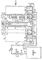
- the plating cell 10 comprises a rectangular tank 12 which is made from a material which is non-conductive and does not interact with the acid plating bath, such as poly (methylmethacrylate) (PMMA) or polypropylene, for example.
- PMMA poly (methylmethacrylate)
- An anode 16 is provided which forms a major part of a wall member which extends from one wall of the tank 12 to the opposite wall.
- the anode 16 is formed of the same metal as the metal to be plated. For example, if copper is to be plated on the wafers, then the anode is made of pure copper or copper with a minor additive, such as 5% phosphorus to improve grain size control, for example.
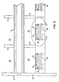
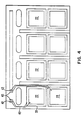
- the embodiment of the cathode assembly 14 shown in the drawings comprises a holder 18 which extends from one wall of tank 12 to the opposite wall of the tank in a vertically extending plane that is substantially parallel to the anode 16 to form a channel 20 through which the plating bath is directed vertically upward in a laminar flow.
- Holder 18 mounts a plurality of wafers 22 upon which a metallic coating is to be electroplated.
- the wafers are formed of a suitable substrate material such as a ceramic material, for example, and one surface 24 of the wafers 22 is coated with a thin film conductive coating of the same material as the material to be plated by vacuum deposition, E beam deposition or sputtering, for example.
- Holder 18 is made from a non-conductive material which does not react with the acidic plating bath such as PMMA or polypropylene, and has a plurality of openings 26 into which the wafers 22 are mounted in a fixed position. Each of the openings 26 has a reduced area lip 28 (FIG. 3) against which one of the wafers is mounted in a position so that a seal is formed to prevent the plating bath from contacting the sides or rear surface of the wafer.
- a non-conductive material which does not react with the acidic plating bath such as PMMA or polypropylene
- Conductive gasket 38 is designed to provide a uniform peripheral contact to the thin conductive coating on surface 24 of wafers 22.
- Conductive gasket 38 may comprise a thin conductive metal such as stainless steel, brass or berryllium copper. In this case, the gasket 38 is shaped by punching or machining, is flat annealed after shaping and then gold plated to minimize dissolution of the gasket material in the plating bath.
- conductive gasket 38 may be made from a conductive elastomer such as a silver loaded silicone rubber material, for example.
- a conductor 40 is included within holder 18 which extends from a position in contact with conductive gasket 38 to a terminal 42 to which a suitable power supply connection can be made.
- the power supply 44 is connected between the anode 16 and the terminals 42, one of which is provided for each wafer 22 of cathode assembly 14.
- a short wall member 41 is provided which extends from the anode 16 toward the cathode 14 so that, when the cathode assembly 14 is in place, a channel 20' is provided for each two wafers 22.
- This structure has the advantage that each pair of wafers 22 can be controlled to different characteristics, if desired.
- This construction has the additional advantage that the number of wafers to be plated can be varied in increments of two wafers from two up to the maximum capacity of the cell and still retain the characteristics of uniform thickness plating.
- a blank piece of an inert material such as glass which has the same size as that of the wafers is inserted into openings 26 to close these openings and thereby maintain the laminar flow of plating bath.
- a thieving ring 39 may be provided surrounding each wafer 22, and in that case a further terminal 43 is provided for each wafer 22 of the cathode assembly 14.
- a thieving ring 39 is a conductive element which surrounds the wafer 22, and is operable to produce a greater uniformity control.
- a variable resistor is connected in the circuit from power supply to the thieving ring 39 and a second variable resistor is connected in the circuit from the power supply 44 to the wafer 22. The variable resistors are adjusted prior to the plating operation to maintain a constant preselected current bias ratio between the wafer 22 and thieving ring 39 during the plating process.
- the plating bath is supplied to inlet 58 of cell 10 from a suitable reservoir 46 by means of tube 48, pump 50, filter 52, pressure regulator 54 and tube 56.
- the inlet 58 comprises a common manifold which supplies plating bath under pressure to an isostatic chamber 60 which produces, at its output side, a laminar flow of plating bath which has uniform flow across each channel 20'.
- the isostatic chamber 60 is separated from inlet 58 by means of a perforated plate 62 having openings from 2 to 4 mm, for example, which serves to distribute the flow across the chamber.
- the isostatic chamber is filled with a plurality of generally spherical beads 64, the size of which is chosen to produce the desired flow through channel 20. In a particular application, glass beads in the range of 4 to 6 mm worked well. Beads 64 are made from an inert material such as glass or Teflon (Registered Trade Mark), and these beads 64 are held in position by means of a thin membrane member 66.
- Membrane 66 has a plurality of spaced orifices 68 to form a fine mesh screen so that a laminar flow of the plating bath is produced having substantially equal flow at the output end of the isostatic chamber 60.
- a teflon screen with orifices within the range of 10 to 25 Il m was used.
- a shaped deflector 68 is provided to direct the plating bath in a substantially vertical laminar flow which has a substantially equal flow across the width of channel 20.
- the continuous vertical flow has the advantage that any hydrogen gas and/or any particulate material formed during the plating operation is/are swept away from the face of the article to be plated. This sweeping action prevents voids from forming in the plated film due to hydrogen gas bubble accumulation or due to other causes.
- the plating cell 10 is operated by inserting cathode 14 through openings 11 in the cover 15 of tank 12 to produce a sealed enclosure with the side walls 13 of tank 12. Flow of the plating bath is started, and the level of plating bath in channels 20 rises until the level reaches openings 17 in holder 18 and openings 19 in anode 16. Openings 17 and 19 are past the wafers 22 in the vertical direction so that a laminar flow will be present for all areas to be plated. The plating bath overflows through openings 17 and 19 to a sump 21 from which the plating bath is returned through tube 57 to the reservoir 46 for treatment for temperature and pH control, for example.
- the continuous flow of the plating bath through the plating cell is continued for a predetermined time which is chosen so that the acid plating bath removes any oxidation from the cathode and the anode and to provide the time required for the system to reach thermal equilibrium.
- the current from power supply 44 is turned ON to both the wafers 22 and thieving rings 39 for a predetermined time based on the thickness to be plated.
- the cathode assembly is removed vertically from the plating cell. Since one wall of channel 20 is opened by this action, the flow of the plating solution is from the isostatic chamber to the sump. The level of the plating solution is below the bottom of the anode member, and, as a result, the plating bath composition is not altered by the continuous dissolution of the anode material by the acidic plating bath during non-plating intervals.
- a plurality of wafers of a ceramic material comprising a mixture of aluminium oxide and titanium carbide with a flash coating of copper sputtered on one face of the wafers was plated with copper with the apparatus of the present invention to provide a plurality of copper patterns thereon.
- the plating bath comprised copper sulphate, sulfuric acid and deionized water to a pH of 2.5.
- the bath was maintained to a temperature of 20 ° C and the continuous flow rate was about 2,27 I (0.6 gallons) per minute.
- copper was deposited at the rate of 0,1 [im (1000 angstroms) per minute.
- the plated copper had a thickness uniformity within a wafer, from wafer to wafer and from batch to batch of better than ⁇ 2%.
- the plated deposits had an average grain size of about 1.5 to 3 ⁇ m, and the high density plating deposits were void free and lamination free.
Landscapes
- Chemical & Material Sciences (AREA)
- Engineering & Computer Science (AREA)
- Chemical Kinetics & Catalysis (AREA)
- Electrochemistry (AREA)
- Materials Engineering (AREA)
- Metallurgy (AREA)
- Organic Chemistry (AREA)
- Life Sciences & Earth Sciences (AREA)
- Sustainable Development (AREA)
- Electroplating Methods And Accessories (AREA)
- Electrodes Of Semiconductors (AREA)
Applications Claiming Priority (2)
| Application Number | Priority Date | Filing Date | Title |
|---|---|---|---|
| US834699 | 1986-02-28 | ||
| US06/834,699 US4696729A (en) | 1986-02-28 | 1986-02-28 | Electroplating cell |
Publications (2)
| Publication Number | Publication Date |
|---|---|
| EP0234212A1 EP0234212A1 (en) | 1987-09-02 |
| EP0234212B1 true EP0234212B1 (en) | 1990-01-03 |
Family
ID=25267571
Family Applications (1)
| Application Number | Title | Priority Date | Filing Date |
|---|---|---|---|
| EP87100343A Expired EP0234212B1 (en) | 1986-02-28 | 1987-01-13 | Electroplating cell |
Country Status (4)
| Country | Link |
|---|---|
| US (1) | US4696729A (enExample) |
| EP (1) | EP0234212B1 (enExample) |
| JP (1) | JPS62207895A (enExample) |
| DE (1) | DE3761314D1 (enExample) |
Families Citing this family (99)
| Publication number | Priority date | Publication date | Assignee | Title |
|---|---|---|---|---|
| US4871435A (en) * | 1988-10-14 | 1989-10-03 | Charles Denofrio | Electroplating apparatus |
| GB8900557D0 (en) * | 1989-01-11 | 1989-03-08 | Atomic Energy Authority Uk | Electrochemical cell |
| US4935108A (en) * | 1989-04-28 | 1990-06-19 | Hewlett-Packard Company | Apparatus for troubleshooting photoimage plating problems in printed circuit board manufacturing |
| US5256565A (en) * | 1989-05-08 | 1993-10-26 | The United States Of America As Represented By The United States Department Of Energy | Electrochemical planarization |
| GB8911566D0 (en) * | 1989-05-19 | 1989-07-05 | Sun Ind Coatings | Plating system |
| US6375741B2 (en) | 1991-03-06 | 2002-04-23 | Timothy J. Reardon | Semiconductor processing spray coating apparatus |
| DE4024576A1 (de) * | 1990-08-02 | 1992-02-06 | Bosch Gmbh Robert | Vorrichtung zum einseitigen aetzen einer halbleiterscheibe |
| US5198089A (en) * | 1991-10-29 | 1993-03-30 | National Semiconductor Corporation | Plating tank |
| JP2888001B2 (ja) * | 1992-01-09 | 1999-05-10 | 日本電気株式会社 | 金属メッキ装置 |
| US5514258A (en) * | 1994-08-18 | 1996-05-07 | Brinket; Oscar J. | Substrate plating device having laminar flow |
| US5516412A (en) * | 1995-05-16 | 1996-05-14 | International Business Machines Corporation | Vertical paddle plating cell |
| US5522975A (en) * | 1995-05-16 | 1996-06-04 | International Business Machines Corporation | Electroplating workpiece fixture |
| US5597460A (en) * | 1995-11-13 | 1997-01-28 | Reynolds Tech Fabricators, Inc. | Plating cell having laminar flow sparger |
| US5620581A (en) * | 1995-11-29 | 1997-04-15 | Aiwa Research And Development, Inc. | Apparatus for electroplating metal films including a cathode ring, insulator ring and thief ring |
| WO2000061498A2 (en) | 1999-04-13 | 2000-10-19 | Semitool, Inc. | System for electrochemically processing a workpiece |
| US5893966A (en) * | 1997-07-28 | 1999-04-13 | Micron Technology, Inc. | Method and apparatus for continuous processing of semiconductor wafers |
| US6033548A (en) * | 1997-07-28 | 2000-03-07 | Micron Technology, Inc. | Rotating system and method for electrodepositing materials on semiconductor wafers |
| US6156167A (en) * | 1997-11-13 | 2000-12-05 | Novellus Systems, Inc. | Clamshell apparatus for electrochemically treating semiconductor wafers |
| US6126798A (en) * | 1997-11-13 | 2000-10-03 | Novellus Systems, Inc. | Electroplating anode including membrane partition system and method of preventing passivation of same |
| US6159354A (en) * | 1997-11-13 | 2000-12-12 | Novellus Systems, Inc. | Electric potential shaping method for electroplating |
| US6179983B1 (en) | 1997-11-13 | 2001-01-30 | Novellus Systems, Inc. | Method and apparatus for treating surface including virtual anode |
| US6027631A (en) * | 1997-11-13 | 2000-02-22 | Novellus Systems, Inc. | Electroplating system with shields for varying thickness profile of deposited layer |
| US6565729B2 (en) | 1998-03-20 | 2003-05-20 | Semitool, Inc. | Method for electrochemically depositing metal on a semiconductor workpiece |
| US6228232B1 (en) | 1998-07-09 | 2001-05-08 | Semitool, Inc. | Reactor vessel having improved cup anode and conductor assembly |
| US6497801B1 (en) | 1998-07-10 | 2002-12-24 | Semitool Inc | Electroplating apparatus with segmented anode array |
| US6919010B1 (en) | 2001-06-28 | 2005-07-19 | Novellus Systems, Inc. | Uniform electroplating of thin metal seeded wafers using rotationally asymmetric variable anode correction |
| US6454918B1 (en) * | 1999-03-23 | 2002-09-24 | Electroplating Engineers Of Japan Limited | Cup type plating apparatus |
| US7264698B2 (en) | 1999-04-13 | 2007-09-04 | Semitool, Inc. | Apparatus and methods for electrochemical processing of microelectronic workpieces |
| US7585398B2 (en) | 1999-04-13 | 2009-09-08 | Semitool, Inc. | Chambers, systems, and methods for electrochemically processing microfeature workpieces |
| US7189318B2 (en) | 1999-04-13 | 2007-03-13 | Semitool, Inc. | Tuning electrodes used in a reactor for electrochemically processing a microelectronic workpiece |
| US7020537B2 (en) | 1999-04-13 | 2006-03-28 | Semitool, Inc. | Tuning electrodes used in a reactor for electrochemically processing a microelectronic workpiece |
| US7438788B2 (en) | 1999-04-13 | 2008-10-21 | Semitool, Inc. | Apparatus and methods for electrochemical processing of microelectronic workpieces |
| US7351314B2 (en) | 2003-12-05 | 2008-04-01 | Semitool, Inc. | Chambers, systems, and methods for electrochemically processing microfeature workpieces |
| US6916412B2 (en) | 1999-04-13 | 2005-07-12 | Semitool, Inc. | Adaptable electrochemical processing chamber |
| US7351315B2 (en) | 2003-12-05 | 2008-04-01 | Semitool, Inc. | Chambers, systems, and methods for electrochemically processing microfeature workpieces |
| KR100293239B1 (ko) * | 1999-06-23 | 2001-06-15 | 김무 | 반도체 기질 도금장치 및 방법 |
| DE19938409C1 (de) * | 1999-08-13 | 2001-03-22 | Tyco Electronics Logistics Ag | Anordnung zum gleichmäßigen Umströmen einer Oberfläche einer Probe mit Flüssigkeit und Verwendung der Anordnung |
| US6278210B1 (en) | 1999-08-30 | 2001-08-21 | International Business Machines Corporation | Rotary element apparatus with wireless power transfer |
| US8308931B2 (en) * | 2006-08-16 | 2012-11-13 | Novellus Systems, Inc. | Method and apparatus for electroplating |
| US8475636B2 (en) | 2008-11-07 | 2013-07-02 | Novellus Systems, Inc. | Method and apparatus for electroplating |
| US6821407B1 (en) * | 2000-05-10 | 2004-11-23 | Novellus Systems, Inc. | Anode and anode chamber for copper electroplating |
| US6527920B1 (en) | 2000-05-10 | 2003-03-04 | Novellus Systems, Inc. | Copper electroplating apparatus |
| US7622024B1 (en) | 2000-05-10 | 2009-11-24 | Novellus Systems, Inc. | High resistance ionic current source |
| US6869515B2 (en) | 2001-03-30 | 2005-03-22 | Uri Cohen | Enhanced electrochemical deposition (ECD) filling of high aspect ratio openings |
| US20060011487A1 (en) * | 2001-05-31 | 2006-01-19 | Surfect Technologies, Inc. | Submicron and nano size particle encapsulation by electrochemical process and apparatus |
| US7682498B1 (en) | 2001-06-28 | 2010-03-23 | Novellus Systems, Inc. | Rotationally asymmetric variable electrode correction |
| US6908540B2 (en) * | 2001-07-13 | 2005-06-21 | Applied Materials, Inc. | Method and apparatus for encapsulation of an edge of a substrate during an electro-chemical deposition process |
| US6818115B2 (en) | 2001-10-19 | 2004-11-16 | Viasystems Group, Inc. | System and method for electrolytic plating |
| JP4011336B2 (ja) * | 2001-12-07 | 2007-11-21 | 日鉱金属株式会社 | 電気銅めっき方法、電気銅めっき用純銅アノード及びこれらを用いてめっきされたパーティクル付着の少ない半導体ウエハ |
| US6841057B2 (en) | 2002-03-13 | 2005-01-11 | Applied Materials Inc. | Method and apparatus for substrate polishing |
| US7854828B2 (en) * | 2006-08-16 | 2010-12-21 | Novellus Systems, Inc. | Method and apparatus for electroplating including remotely positioned second cathode |
| US7118658B2 (en) * | 2002-05-21 | 2006-10-10 | Semitool, Inc. | Electroplating reactor |
| US20050061660A1 (en) * | 2002-10-18 | 2005-03-24 | Kempen Hein Van | System and method for electrolytic plating |
| JP2006513041A (ja) * | 2002-12-05 | 2006-04-20 | サーフェクト テクノロジーズ インク. | コーティングされた磁性粒子及びその応用 |
| WO2004072331A2 (en) * | 2003-02-12 | 2004-08-26 | Surfect Technologies, Inc. | Apparatus and method for highly controlled electrodeposition |
| US20060049038A1 (en) * | 2003-02-12 | 2006-03-09 | Surfect Technologies, Inc. | Dynamic profile anode |
| CN1920105B (zh) * | 2003-10-22 | 2010-12-08 | 内克斯系统公司 | 用于对工件进行流体处理的方法和设备 |
| US7727366B2 (en) * | 2003-10-22 | 2010-06-01 | Nexx Systems, Inc. | Balancing pressure to improve a fluid seal |
| WO2005076977A2 (en) * | 2004-02-04 | 2005-08-25 | Surfect Technologies, Inc. | Plating apparatus and method |
| US7553401B2 (en) * | 2004-03-19 | 2009-06-30 | Faraday Technology, Inc. | Electroplating cell with hydrodynamics facilitating more uniform deposition across a workpiece during plating |
| US7947161B2 (en) * | 2004-03-19 | 2011-05-24 | Faraday Technology, Inc. | Method of operating an electroplating cell with hydrodynamics facilitating more uniform deposition on a workpiece with through holes |
| US8623193B1 (en) | 2004-06-16 | 2014-01-07 | Novellus Systems, Inc. | Method of electroplating using a high resistance ionic current source |
| US20050283993A1 (en) * | 2004-06-18 | 2005-12-29 | Qunwei Wu | Method and apparatus for fluid processing and drying a workpiece |
| US7285195B2 (en) * | 2004-06-24 | 2007-10-23 | Applied Materials, Inc. | Electric field reducing thrust plate |
| US7608174B1 (en) | 2005-04-22 | 2009-10-27 | Sandia Corporation | Apparatus and method for electroforming high aspect ratio micro-parts |
| JP4458057B2 (ja) * | 2005-07-28 | 2010-04-28 | Tdk株式会社 | めっき装置及びめっき方法 |
| TWI314957B (en) * | 2005-12-29 | 2009-09-21 | Ind Tech Res Inst | Apparatus for metal plating on a substrate |
| US9822461B2 (en) | 2006-08-16 | 2017-11-21 | Novellus Systems, Inc. | Dynamic current distribution control apparatus and method for wafer electroplating |
| US7651384B2 (en) * | 2007-01-09 | 2010-01-26 | Applied Materials, Inc. | Method and system for point of use recycling of ECMP fluids |
| US7799684B1 (en) | 2007-03-05 | 2010-09-21 | Novellus Systems, Inc. | Two step process for uniform across wafer deposition and void free filling on ruthenium coated wafers |
| US8012319B2 (en) * | 2007-11-21 | 2011-09-06 | Texas Instruments Incorporated | Multi-chambered metal electrodeposition system for semiconductor substrates |
| US7964506B1 (en) | 2008-03-06 | 2011-06-21 | Novellus Systems, Inc. | Two step copper electroplating process with anneal for uniform across wafer deposition and void free filling on ruthenium coated wafers |
| US8513124B1 (en) | 2008-03-06 | 2013-08-20 | Novellus Systems, Inc. | Copper electroplating process for uniform across wafer deposition and void free filling on semi-noble metal coated wafers |
| US8703615B1 (en) | 2008-03-06 | 2014-04-22 | Novellus Systems, Inc. | Copper electroplating process for uniform across wafer deposition and void free filling on ruthenium coated wafers |
| US8858774B2 (en) | 2008-11-07 | 2014-10-14 | Novellus Systems, Inc. | Electroplating apparatus for tailored uniformity profile |
| US20120261254A1 (en) | 2011-04-15 | 2012-10-18 | Reid Jonathan D | Method and apparatus for filling interconnect structures |
| US8475637B2 (en) * | 2008-12-17 | 2013-07-02 | Novellus Systems, Inc. | Electroplating apparatus with vented electrolyte manifold |
| US8262871B1 (en) | 2008-12-19 | 2012-09-11 | Novellus Systems, Inc. | Plating method and apparatus with multiple internally irrigated chambers |
| US8795480B2 (en) | 2010-07-02 | 2014-08-05 | Novellus Systems, Inc. | Control of electrolyte hydrodynamics for efficient mass transfer during electroplating |
| US9523155B2 (en) | 2012-12-12 | 2016-12-20 | Novellus Systems, Inc. | Enhancement of electrolyte hydrodynamics for efficient mass transfer during electroplating |
| US10233556B2 (en) | 2010-07-02 | 2019-03-19 | Lam Research Corporation | Dynamic modulation of cross flow manifold during electroplating |
| US9624592B2 (en) | 2010-07-02 | 2017-04-18 | Novellus Systems, Inc. | Cross flow manifold for electroplating apparatus |
| US10094034B2 (en) | 2015-08-28 | 2018-10-09 | Lam Research Corporation | Edge flow element for electroplating apparatus |
| US9909228B2 (en) | 2012-11-27 | 2018-03-06 | Lam Research Corporation | Method and apparatus for dynamic current distribution control during electroplating |
| US9670588B2 (en) | 2013-05-01 | 2017-06-06 | Lam Research Corporation | Anisotropic high resistance ionic current source (AHRICS) |
| US9449808B2 (en) | 2013-05-29 | 2016-09-20 | Novellus Systems, Inc. | Apparatus for advanced packaging applications |
| US9677190B2 (en) | 2013-11-01 | 2017-06-13 | Lam Research Corporation | Membrane design for reducing defects in electroplating systems |
| US9752248B2 (en) | 2014-12-19 | 2017-09-05 | Lam Research Corporation | Methods and apparatuses for dynamically tunable wafer-edge electroplating |
| US9567685B2 (en) | 2015-01-22 | 2017-02-14 | Lam Research Corporation | Apparatus and method for dynamic control of plated uniformity with the use of remote electric current |
| US9816194B2 (en) | 2015-03-19 | 2017-11-14 | Lam Research Corporation | Control of electrolyte flow dynamics for uniform electroplating |
| US10014170B2 (en) | 2015-05-14 | 2018-07-03 | Lam Research Corporation | Apparatus and method for electrodeposition of metals with the use of an ionically resistive ionically permeable element having spatially tailored resistivity |
| US9988733B2 (en) | 2015-06-09 | 2018-06-05 | Lam Research Corporation | Apparatus and method for modulating azimuthal uniformity in electroplating |
| CN105648507A (zh) * | 2016-03-24 | 2016-06-08 | 河南理工大学 | 一种用于电沉积平面件的装置 |
| JP6462620B2 (ja) * | 2016-03-29 | 2019-01-30 | 東京エレクトロン株式会社 | 基板処理装置および基板処理方法 |
| US10364505B2 (en) | 2016-05-24 | 2019-07-30 | Lam Research Corporation | Dynamic modulation of cross flow manifold during elecroplating |
| CN106824581A (zh) * | 2017-02-17 | 2017-06-13 | 张薄 | 一种静电吸附镀膜装置及静电吸附镀膜方法 |
| US11001934B2 (en) | 2017-08-21 | 2021-05-11 | Lam Research Corporation | Methods and apparatus for flow isolation and focusing during electroplating |
| US10781527B2 (en) | 2017-09-18 | 2020-09-22 | Lam Research Corporation | Methods and apparatus for controlling delivery of cross flowing and impinging electrolyte during electroplating |
| CN110541180B (zh) * | 2019-10-12 | 2020-08-18 | 深圳市宜诺自动化设备有限公司 | 一种具有阳极导电装置的铝箔连续氧化设备 |
Family Cites Families (10)
| Publication number | Priority date | Publication date | Assignee | Title |
|---|---|---|---|---|
| US3458421A (en) * | 1966-07-15 | 1969-07-29 | Ibm | Electrode with integral flow channel |
| US3477051A (en) * | 1967-12-26 | 1969-11-04 | Ibm | Die casting of core windings |
| US3933615A (en) * | 1969-06-09 | 1976-01-20 | The United States Of America As Represented By The Secretary Of The Air Force | Fluid flow stripping and plating system |
| US4085010A (en) * | 1974-01-22 | 1978-04-18 | Suzuki Motor Company Limited | Process for powder-dispersed composite plating |
| US4053377A (en) * | 1976-02-13 | 1977-10-11 | The United States Of America As Represented By The Secretary Of The Interior | Electrodeposition of copper |
| US4102756A (en) * | 1976-12-30 | 1978-07-25 | International Business Machines Corporation | Nickel-iron (80:20) alloy thin film electroplating method and electrochemical treatment and plating apparatus |
| US4139429A (en) * | 1978-06-15 | 1979-02-13 | Dart Industries Inc. | Electrolytic cell |
| US4385967A (en) * | 1981-10-07 | 1983-05-31 | Chemcut Corporation | Electroplating apparatus and method |
| US4376031A (en) * | 1982-03-31 | 1983-03-08 | Rca Corporation | Apparatus for electrophoretic deposition |
| DE3317970A1 (de) * | 1983-05-13 | 1984-11-15 | Schering AG, 1000 Berlin und 4709 Bergkamen | Vorrichtung und verfahren zur galvanischen abscheidung von metallen |
-
1986
- 1986-02-28 US US06/834,699 patent/US4696729A/en not_active Expired - Lifetime
- 1986-11-19 JP JP61274264A patent/JPS62207895A/ja active Granted
-
1987
- 1987-01-13 DE DE8787100343T patent/DE3761314D1/de not_active Expired - Lifetime
- 1987-01-13 EP EP87100343A patent/EP0234212B1/en not_active Expired
Also Published As
| Publication number | Publication date |
|---|---|
| US4696729A (en) | 1987-09-29 |
| JPS62207895A (ja) | 1987-09-12 |
| JPH0251994B2 (enExample) | 1990-11-09 |
| DE3761314D1 (de) | 1990-02-08 |
| EP0234212A1 (en) | 1987-09-02 |
Similar Documents
| Publication | Publication Date | Title |
|---|---|---|
| EP0234212B1 (en) | Electroplating cell | |
| US5893966A (en) | Method and apparatus for continuous processing of semiconductor wafers | |
| US6033548A (en) | Rotating system and method for electrodepositing materials on semiconductor wafers | |
| US5391285A (en) | Adjustable plating cell for uniform bump plating of semiconductor wafers | |
| US6989084B2 (en) | Semiconductor wafer plating cell assembly | |
| US5932077A (en) | Plating cell with horizontal product load mechanism | |
| US6521102B1 (en) | Perforated anode for uniform deposition of a metal layer | |
| US20030038035A1 (en) | Methods and systems for controlling current in electrochemical processing of microelectronic workpieces | |
| US3616286A (en) | Automatic process and apparatus for uniform electroplating within porous structures | |
| US4043891A (en) | Electrolytic cell with bipolar electrodes | |
| US4360410A (en) | Electroplating processes and equipment utilizing a foam electrolyte | |
| US20040256222A1 (en) | Apparatus and method for highly controlled electrodeposition | |
| US7090751B2 (en) | Apparatus and methods for electrochemical processing of microelectronic workpieces | |
| KR101077000B1 (ko) | 전기도금용 애노드 | |
| US20060049038A1 (en) | Dynamic profile anode | |
| US4935109A (en) | Double-cell electroplating apparatus and method | |
| EP2652178B1 (en) | Electrochemical deposition apparatus | |
| US5198089A (en) | Plating tank | |
| WO2002033152A1 (en) | A reactor for electrochemically processing a microelectronic workpiece including improved electrode assembly | |
| US6768194B2 (en) | Electrode for electroplating planar structures | |
| US7014739B2 (en) | Convex profile anode for electroplating system | |
| WO2003085713A1 (en) | Homogeneous copper-tin alloy plating for enhancement of electro-migration resistance in interconnects | |
| US20050121329A1 (en) | Thrust pad assembly for ECP system | |
| US4916098A (en) | Process and apparatus for manufacturing an electrocatalytic electrode | |
| WO1990004051A1 (en) | Electroplating process and apparatus |
Legal Events
| Date | Code | Title | Description |
|---|---|---|---|
| PUAI | Public reference made under article 153(3) epc to a published international application that has entered the european phase |
Free format text: ORIGINAL CODE: 0009012 |
|
| AK | Designated contracting states |
Kind code of ref document: A1 Designated state(s): DE FR GB IT |
|
| 17P | Request for examination filed |
Effective date: 19871211 |
|
| 17Q | First examination report despatched |
Effective date: 19890412 |
|
| GRAA | (expected) grant |
Free format text: ORIGINAL CODE: 0009210 |
|
| AK | Designated contracting states |
Kind code of ref document: B1 Designated state(s): DE FR GB IT |
|
| REF | Corresponds to: |
Ref document number: 3761314 Country of ref document: DE Date of ref document: 19900208 |
|
| ET | Fr: translation filed | ||
| ITF | It: translation for a ep patent filed | ||
| PLBE | No opposition filed within time limit |
Free format text: ORIGINAL CODE: 0009261 |
|
| STAA | Information on the status of an ep patent application or granted ep patent |
Free format text: STATUS: NO OPPOSITION FILED WITHIN TIME LIMIT |
|
| 26N | No opposition filed | ||
| ITTA | It: last paid annual fee | ||
| PGFP | Annual fee paid to national office [announced via postgrant information from national office to epo] |
Ref country code: GB Payment date: 19951215 Year of fee payment: 10 |
|
| PGFP | Annual fee paid to national office [announced via postgrant information from national office to epo] |
Ref country code: FR Payment date: 19960103 Year of fee payment: 10 |
|
| PGFP | Annual fee paid to national office [announced via postgrant information from national office to epo] |
Ref country code: DE Payment date: 19960126 Year of fee payment: 10 |
|
| PG25 | Lapsed in a contracting state [announced via postgrant information from national office to epo] |
Ref country code: GB Effective date: 19970113 |
|
| GBPC | Gb: european patent ceased through non-payment of renewal fee |
Effective date: 19970113 |
|
| PG25 | Lapsed in a contracting state [announced via postgrant information from national office to epo] |
Ref country code: FR Effective date: 19970930 |
|
| PG25 | Lapsed in a contracting state [announced via postgrant information from national office to epo] |
Ref country code: DE Effective date: 19971001 |
|
| REG | Reference to a national code |
Ref country code: FR Ref legal event code: ST |
|
| PG25 | Lapsed in a contracting state [announced via postgrant information from national office to epo] |
Ref country code: IT Free format text: LAPSE BECAUSE OF NON-PAYMENT OF DUE FEES Effective date: 20050113 |