EP0228953B1 - Verkapselungsgehäuse für eine elektronische Schaltung - Google Patents
Verkapselungsgehäuse für eine elektronische Schaltung Download PDFInfo
- Publication number
- EP0228953B1 EP0228953B1 EP86402788A EP86402788A EP0228953B1 EP 0228953 B1 EP0228953 B1 EP 0228953B1 EP 86402788 A EP86402788 A EP 86402788A EP 86402788 A EP86402788 A EP 86402788A EP 0228953 B1 EP0228953 B1 EP 0228953B1
- Authority
- EP
- European Patent Office
- Prior art keywords
- circuit
- cover
- box according
- box
- base plate
- Prior art date
- Legal status (The legal status is an assumption and is not a legal conclusion. Google has not performed a legal analysis and makes no representation as to the accuracy of the status listed.)
- Expired - Lifetime
Links
- 238000005538 encapsulation Methods 0.000 title claims description 15
- 239000003990 capacitor Substances 0.000 claims description 9
- 230000000284 resting effect Effects 0.000 claims 1
- 208000032825 Ring chromosome 2 syndrome Diseases 0.000 description 19
- 239000004065 semiconductor Substances 0.000 description 16
- 230000002093 peripheral effect Effects 0.000 description 12
- 238000004519 manufacturing process Methods 0.000 description 7
- 239000000463 material Substances 0.000 description 7
- 239000000758 substrate Substances 0.000 description 7
- 239000004020 conductor Substances 0.000 description 6
- PNEYBMLMFCGWSK-UHFFFAOYSA-N aluminium oxide Inorganic materials [O-2].[O-2].[O-2].[Al+3].[Al+3] PNEYBMLMFCGWSK-UHFFFAOYSA-N 0.000 description 3
- 239000002184 metal Substances 0.000 description 3
- 229910052751 metal Inorganic materials 0.000 description 3
- 238000007789 sealing Methods 0.000 description 3
- 230000000694 effects Effects 0.000 description 2
- 239000008393 encapsulating agent Substances 0.000 description 2
- 238000005516 engineering process Methods 0.000 description 2
- 244000045947 parasite Species 0.000 description 2
- 230000003071 parasitic effect Effects 0.000 description 2
- 238000010396 two-hybrid screening Methods 0.000 description 2
- XUIMIQQOPSSXEZ-UHFFFAOYSA-N Silicon Chemical compound [Si] XUIMIQQOPSSXEZ-UHFFFAOYSA-N 0.000 description 1
- 241001639412 Verres Species 0.000 description 1
- NEIHULKJZQTQKJ-UHFFFAOYSA-N [Cu].[Ag] Chemical compound [Cu].[Ag] NEIHULKJZQTQKJ-UHFFFAOYSA-N 0.000 description 1
- 230000003416 augmentation Effects 0.000 description 1
- 239000002131 composite material Substances 0.000 description 1
- 238000001816 cooling Methods 0.000 description 1
- 230000001186 cumulative effect Effects 0.000 description 1
- 230000007423 decrease Effects 0.000 description 1
- 230000001934 delay Effects 0.000 description 1
- 238000010586 diagram Methods 0.000 description 1
- 239000011521 glass Substances 0.000 description 1
- 230000009931 harmful effect Effects 0.000 description 1
- 230000036039 immunity Effects 0.000 description 1
- 238000000034 method Methods 0.000 description 1
- 230000005855 radiation Effects 0.000 description 1
- 229910052710 silicon Inorganic materials 0.000 description 1
- 239000010703 silicon Substances 0.000 description 1
- 229910000679 solder Inorganic materials 0.000 description 1
Images


Classifications
-
- H—ELECTRICITY
- H01—ELECTRIC ELEMENTS
- H01L—SEMICONDUCTOR DEVICES NOT COVERED BY CLASS H10
- H01L25/00—Assemblies consisting of a plurality of individual semiconductor or other solid state devices ; Multistep manufacturing processes thereof
- H01L25/16—Assemblies consisting of a plurality of individual semiconductor or other solid state devices ; Multistep manufacturing processes thereof the devices being of types provided for in two or more different main groups of groups H01L27/00 - H01L33/00, or in a single subclass of H10K, H10N, e.g. forming hybrid circuits
-
- H—ELECTRICITY
- H01—ELECTRIC ELEMENTS
- H01L—SEMICONDUCTOR DEVICES NOT COVERED BY CLASS H10
- H01L23/00—Details of semiconductor or other solid state devices
- H01L23/02—Containers; Seals
- H01L23/04—Containers; Seals characterised by the shape of the container or parts, e.g. caps, walls
- H01L23/053—Containers; Seals characterised by the shape of the container or parts, e.g. caps, walls the container being a hollow construction and having an insulating or insulated base as a mounting for the semiconductor body
- H01L23/057—Containers; Seals characterised by the shape of the container or parts, e.g. caps, walls the container being a hollow construction and having an insulating or insulated base as a mounting for the semiconductor body the leads being parallel to the base
-
- H—ELECTRICITY
- H01—ELECTRIC ELEMENTS
- H01L—SEMICONDUCTOR DEVICES NOT COVERED BY CLASS H10
- H01L23/00—Details of semiconductor or other solid state devices
- H01L23/52—Arrangements for conducting electric current within the device in operation from one component to another, i.e. interconnections, e.g. wires, lead frames
- H01L23/538—Arrangements for conducting electric current within the device in operation from one component to another, i.e. interconnections, e.g. wires, lead frames the interconnection structure between a plurality of semiconductor chips being formed on, or in, insulating substrates
- H01L23/5383—Multilayer substrates
-
- H—ELECTRICITY
- H01—ELECTRIC ELEMENTS
- H01L—SEMICONDUCTOR DEVICES NOT COVERED BY CLASS H10
- H01L23/00—Details of semiconductor or other solid state devices
- H01L23/58—Structural electrical arrangements for semiconductor devices not otherwise provided for, e.g. in combination with batteries
- H01L23/64—Impedance arrangements
- H01L23/642—Capacitive arrangements
-
- H—ELECTRICITY
- H01—ELECTRIC ELEMENTS
- H01L—SEMICONDUCTOR DEVICES NOT COVERED BY CLASS H10
- H01L25/00—Assemblies consisting of a plurality of individual semiconductor or other solid state devices ; Multistep manufacturing processes thereof
- H01L25/03—Assemblies consisting of a plurality of individual semiconductor or other solid state devices ; Multistep manufacturing processes thereof all the devices being of a type provided for in the same subgroup of groups H01L27/00 - H01L33/00, or in a single subclass of H10K, H10N, e.g. assemblies of rectifier diodes
- H01L25/04—Assemblies consisting of a plurality of individual semiconductor or other solid state devices ; Multistep manufacturing processes thereof all the devices being of a type provided for in the same subgroup of groups H01L27/00 - H01L33/00, or in a single subclass of H10K, H10N, e.g. assemblies of rectifier diodes the devices not having separate containers
- H01L25/065—Assemblies consisting of a plurality of individual semiconductor or other solid state devices ; Multistep manufacturing processes thereof all the devices being of a type provided for in the same subgroup of groups H01L27/00 - H01L33/00, or in a single subclass of H10K, H10N, e.g. assemblies of rectifier diodes the devices not having separate containers the devices being of a type provided for in group H01L27/00
- H01L25/0652—Assemblies consisting of a plurality of individual semiconductor or other solid state devices ; Multistep manufacturing processes thereof all the devices being of a type provided for in the same subgroup of groups H01L27/00 - H01L33/00, or in a single subclass of H10K, H10N, e.g. assemblies of rectifier diodes the devices not having separate containers the devices being of a type provided for in group H01L27/00 the devices being arranged next and on each other, i.e. mixed assemblies
-
- H—ELECTRICITY
- H01—ELECTRIC ELEMENTS
- H01L—SEMICONDUCTOR DEVICES NOT COVERED BY CLASS H10
- H01L25/00—Assemblies consisting of a plurality of individual semiconductor or other solid state devices ; Multistep manufacturing processes thereof
- H01L25/03—Assemblies consisting of a plurality of individual semiconductor or other solid state devices ; Multistep manufacturing processes thereof all the devices being of a type provided for in the same subgroup of groups H01L27/00 - H01L33/00, or in a single subclass of H10K, H10N, e.g. assemblies of rectifier diodes
- H01L25/04—Assemblies consisting of a plurality of individual semiconductor or other solid state devices ; Multistep manufacturing processes thereof all the devices being of a type provided for in the same subgroup of groups H01L27/00 - H01L33/00, or in a single subclass of H10K, H10N, e.g. assemblies of rectifier diodes the devices not having separate containers
- H01L25/065—Assemblies consisting of a plurality of individual semiconductor or other solid state devices ; Multistep manufacturing processes thereof all the devices being of a type provided for in the same subgroup of groups H01L27/00 - H01L33/00, or in a single subclass of H10K, H10N, e.g. assemblies of rectifier diodes the devices not having separate containers the devices being of a type provided for in group H01L27/00
- H01L25/0655—Assemblies consisting of a plurality of individual semiconductor or other solid state devices ; Multistep manufacturing processes thereof all the devices being of a type provided for in the same subgroup of groups H01L27/00 - H01L33/00, or in a single subclass of H10K, H10N, e.g. assemblies of rectifier diodes the devices not having separate containers the devices being of a type provided for in group H01L27/00 the devices being arranged next to each other
-
- H—ELECTRICITY
- H01—ELECTRIC ELEMENTS
- H01L—SEMICONDUCTOR DEVICES NOT COVERED BY CLASS H10
- H01L2224/00—Indexing scheme for arrangements for connecting or disconnecting semiconductor or solid-state bodies and methods related thereto as covered by H01L24/00
- H01L2224/01—Means for bonding being attached to, or being formed on, the surface to be connected, e.g. chip-to-package, die-attach, "first-level" interconnects; Manufacturing methods related thereto
- H01L2224/26—Layer connectors, e.g. plate connectors, solder or adhesive layers; Manufacturing methods related thereto
- H01L2224/31—Structure, shape, material or disposition of the layer connectors after the connecting process
- H01L2224/32—Structure, shape, material or disposition of the layer connectors after the connecting process of an individual layer connector
- H01L2224/321—Disposition
- H01L2224/32151—Disposition the layer connector connecting between a semiconductor or solid-state body and an item not being a semiconductor or solid-state body, e.g. chip-to-substrate, chip-to-passive
- H01L2224/32221—Disposition the layer connector connecting between a semiconductor or solid-state body and an item not being a semiconductor or solid-state body, e.g. chip-to-substrate, chip-to-passive the body and the item being stacked
- H01L2224/32225—Disposition the layer connector connecting between a semiconductor or solid-state body and an item not being a semiconductor or solid-state body, e.g. chip-to-substrate, chip-to-passive the body and the item being stacked the item being non-metallic, e.g. insulating substrate with or without metallisation
-
- H—ELECTRICITY
- H01—ELECTRIC ELEMENTS
- H01L—SEMICONDUCTOR DEVICES NOT COVERED BY CLASS H10
- H01L2224/00—Indexing scheme for arrangements for connecting or disconnecting semiconductor or solid-state bodies and methods related thereto as covered by H01L24/00
- H01L2224/01—Means for bonding being attached to, or being formed on, the surface to be connected, e.g. chip-to-package, die-attach, "first-level" interconnects; Manufacturing methods related thereto
- H01L2224/42—Wire connectors; Manufacturing methods related thereto
- H01L2224/44—Structure, shape, material or disposition of the wire connectors prior to the connecting process
- H01L2224/45—Structure, shape, material or disposition of the wire connectors prior to the connecting process of an individual wire connector
- H01L2224/45001—Core members of the connector
- H01L2224/4501—Shape
- H01L2224/45012—Cross-sectional shape
- H01L2224/45014—Ribbon connectors, e.g. rectangular cross-section
-
- H—ELECTRICITY
- H01—ELECTRIC ELEMENTS
- H01L—SEMICONDUCTOR DEVICES NOT COVERED BY CLASS H10
- H01L2224/00—Indexing scheme for arrangements for connecting or disconnecting semiconductor or solid-state bodies and methods related thereto as covered by H01L24/00
- H01L2224/01—Means for bonding being attached to, or being formed on, the surface to be connected, e.g. chip-to-package, die-attach, "first-level" interconnects; Manufacturing methods related thereto
- H01L2224/42—Wire connectors; Manufacturing methods related thereto
- H01L2224/47—Structure, shape, material or disposition of the wire connectors after the connecting process
- H01L2224/48—Structure, shape, material or disposition of the wire connectors after the connecting process of an individual wire connector
- H01L2224/4805—Shape
- H01L2224/4809—Loop shape
- H01L2224/48091—Arched
-
- H—ELECTRICITY
- H01—ELECTRIC ELEMENTS
- H01L—SEMICONDUCTOR DEVICES NOT COVERED BY CLASS H10
- H01L2224/00—Indexing scheme for arrangements for connecting or disconnecting semiconductor or solid-state bodies and methods related thereto as covered by H01L24/00
- H01L2224/01—Means for bonding being attached to, or being formed on, the surface to be connected, e.g. chip-to-package, die-attach, "first-level" interconnects; Manufacturing methods related thereto
- H01L2224/42—Wire connectors; Manufacturing methods related thereto
- H01L2224/47—Structure, shape, material or disposition of the wire connectors after the connecting process
- H01L2224/48—Structure, shape, material or disposition of the wire connectors after the connecting process of an individual wire connector
- H01L2224/481—Disposition
- H01L2224/48151—Connecting between a semiconductor or solid-state body and an item not being a semiconductor or solid-state body, e.g. chip-to-substrate, chip-to-passive
- H01L2224/48221—Connecting between a semiconductor or solid-state body and an item not being a semiconductor or solid-state body, e.g. chip-to-substrate, chip-to-passive the body and the item being stacked
- H01L2224/48225—Connecting between a semiconductor or solid-state body and an item not being a semiconductor or solid-state body, e.g. chip-to-substrate, chip-to-passive the body and the item being stacked the item being non-metallic, e.g. insulating substrate with or without metallisation
- H01L2224/48227—Connecting between a semiconductor or solid-state body and an item not being a semiconductor or solid-state body, e.g. chip-to-substrate, chip-to-passive the body and the item being stacked the item being non-metallic, e.g. insulating substrate with or without metallisation connecting the wire to a bond pad of the item
-
- H—ELECTRICITY
- H01—ELECTRIC ELEMENTS
- H01L—SEMICONDUCTOR DEVICES NOT COVERED BY CLASS H10
- H01L2224/00—Indexing scheme for arrangements for connecting or disconnecting semiconductor or solid-state bodies and methods related thereto as covered by H01L24/00
- H01L2224/73—Means for bonding being of different types provided for in two or more of groups H01L2224/10, H01L2224/18, H01L2224/26, H01L2224/34, H01L2224/42, H01L2224/50, H01L2224/63, H01L2224/71
- H01L2224/732—Location after the connecting process
- H01L2224/73251—Location after the connecting process on different surfaces
- H01L2224/73265—Layer and wire connectors
-
- H—ELECTRICITY
- H01—ELECTRIC ELEMENTS
- H01L—SEMICONDUCTOR DEVICES NOT COVERED BY CLASS H10
- H01L24/00—Arrangements for connecting or disconnecting semiconductor or solid-state bodies; Methods or apparatus related thereto
- H01L24/01—Means for bonding being attached to, or being formed on, the surface to be connected, e.g. chip-to-package, die-attach, "first-level" interconnects; Manufacturing methods related thereto
- H01L24/42—Wire connectors; Manufacturing methods related thereto
- H01L24/47—Structure, shape, material or disposition of the wire connectors after the connecting process
- H01L24/48—Structure, shape, material or disposition of the wire connectors after the connecting process of an individual wire connector
-
- H—ELECTRICITY
- H01—ELECTRIC ELEMENTS
- H01L—SEMICONDUCTOR DEVICES NOT COVERED BY CLASS H10
- H01L2924/00—Indexing scheme for arrangements or methods for connecting or disconnecting semiconductor or solid-state bodies as covered by H01L24/00
- H01L2924/0001—Technical content checked by a classifier
- H01L2924/00014—Technical content checked by a classifier the subject-matter covered by the group, the symbol of which is combined with the symbol of this group, being disclosed without further technical details
-
- H—ELECTRICITY
- H01—ELECTRIC ELEMENTS
- H01L—SEMICONDUCTOR DEVICES NOT COVERED BY CLASS H10
- H01L2924/00—Indexing scheme for arrangements or methods for connecting or disconnecting semiconductor or solid-state bodies as covered by H01L24/00
- H01L2924/01—Chemical elements
- H01L2924/01014—Silicon [Si]
-
- H—ELECTRICITY
- H01—ELECTRIC ELEMENTS
- H01L—SEMICONDUCTOR DEVICES NOT COVERED BY CLASS H10
- H01L2924/00—Indexing scheme for arrangements or methods for connecting or disconnecting semiconductor or solid-state bodies as covered by H01L24/00
- H01L2924/01—Chemical elements
- H01L2924/01079—Gold [Au]
-
- H—ELECTRICITY
- H01—ELECTRIC ELEMENTS
- H01L—SEMICONDUCTOR DEVICES NOT COVERED BY CLASS H10
- H01L2924/00—Indexing scheme for arrangements or methods for connecting or disconnecting semiconductor or solid-state bodies as covered by H01L24/00
- H01L2924/10—Details of semiconductor or other solid state devices to be connected
- H01L2924/102—Material of the semiconductor or solid state bodies
- H01L2924/1025—Semiconducting materials
- H01L2924/10251—Elemental semiconductors, i.e. Group IV
- H01L2924/10253—Silicon [Si]
-
- H—ELECTRICITY
- H01—ELECTRIC ELEMENTS
- H01L—SEMICONDUCTOR DEVICES NOT COVERED BY CLASS H10
- H01L2924/00—Indexing scheme for arrangements or methods for connecting or disconnecting semiconductor or solid-state bodies as covered by H01L24/00
- H01L2924/10—Details of semiconductor or other solid state devices to be connected
- H01L2924/11—Device type
- H01L2924/14—Integrated circuits
-
- H—ELECTRICITY
- H01—ELECTRIC ELEMENTS
- H01L—SEMICONDUCTOR DEVICES NOT COVERED BY CLASS H10
- H01L2924/00—Indexing scheme for arrangements or methods for connecting or disconnecting semiconductor or solid-state bodies as covered by H01L24/00
- H01L2924/15—Details of package parts other than the semiconductor or other solid state devices to be connected
- H01L2924/151—Die mounting substrate
- H01L2924/1515—Shape
- H01L2924/15153—Shape the die mounting substrate comprising a recess for hosting the device
-
- H—ELECTRICITY
- H01—ELECTRIC ELEMENTS
- H01L—SEMICONDUCTOR DEVICES NOT COVERED BY CLASS H10
- H01L2924/00—Indexing scheme for arrangements or methods for connecting or disconnecting semiconductor or solid-state bodies as covered by H01L24/00
- H01L2924/15—Details of package parts other than the semiconductor or other solid state devices to be connected
- H01L2924/151—Die mounting substrate
- H01L2924/1517—Multilayer substrate
-
- H—ELECTRICITY
- H01—ELECTRIC ELEMENTS
- H01L—SEMICONDUCTOR DEVICES NOT COVERED BY CLASS H10
- H01L2924/00—Indexing scheme for arrangements or methods for connecting or disconnecting semiconductor or solid-state bodies as covered by H01L24/00
- H01L2924/15—Details of package parts other than the semiconductor or other solid state devices to be connected
- H01L2924/161—Cap
- H01L2924/1615—Shape
- H01L2924/16195—Flat cap [not enclosing an internal cavity]
-
- H—ELECTRICITY
- H01—ELECTRIC ELEMENTS
- H01L—SEMICONDUCTOR DEVICES NOT COVERED BY CLASS H10
- H01L2924/00—Indexing scheme for arrangements or methods for connecting or disconnecting semiconductor or solid-state bodies as covered by H01L24/00
- H01L2924/15—Details of package parts other than the semiconductor or other solid state devices to be connected
- H01L2924/161—Cap
- H01L2924/162—Disposition
- H01L2924/1627—Disposition stacked type assemblies, e.g. stacked multi-cavities
-
- H—ELECTRICITY
- H01—ELECTRIC ELEMENTS
- H01L—SEMICONDUCTOR DEVICES NOT COVERED BY CLASS H10
- H01L2924/00—Indexing scheme for arrangements or methods for connecting or disconnecting semiconductor or solid-state bodies as covered by H01L24/00
- H01L2924/19—Details of hybrid assemblies other than the semiconductor or other solid state devices to be connected
- H01L2924/1901—Structure
- H01L2924/1904—Component type
- H01L2924/19041—Component type being a capacitor
-
- H—ELECTRICITY
- H01—ELECTRIC ELEMENTS
- H01L—SEMICONDUCTOR DEVICES NOT COVERED BY CLASS H10
- H01L2924/00—Indexing scheme for arrangements or methods for connecting or disconnecting semiconductor or solid-state bodies as covered by H01L24/00
- H01L2924/30—Technical effects
- H01L2924/301—Electrical effects
- H01L2924/30107—Inductance
-
- H—ELECTRICITY
- H01—ELECTRIC ELEMENTS
- H01L—SEMICONDUCTOR DEVICES NOT COVERED BY CLASS H10
- H01L2924/00—Indexing scheme for arrangements or methods for connecting or disconnecting semiconductor or solid-state bodies as covered by H01L24/00
- H01L2924/30—Technical effects
- H01L2924/301—Electrical effects
- H01L2924/3011—Impedance
-
- Y—GENERAL TAGGING OF NEW TECHNOLOGICAL DEVELOPMENTS; GENERAL TAGGING OF CROSS-SECTIONAL TECHNOLOGIES SPANNING OVER SEVERAL SECTIONS OF THE IPC; TECHNICAL SUBJECTS COVERED BY FORMER USPC CROSS-REFERENCE ART COLLECTIONS [XRACs] AND DIGESTS
- Y10—TECHNICAL SUBJECTS COVERED BY FORMER USPC
- Y10S—TECHNICAL SUBJECTS COVERED BY FORMER USPC CROSS-REFERENCE ART COLLECTIONS [XRACs] AND DIGESTS
- Y10S257/00—Active solid-state devices, e.g. transistors, solid-state diodes
- Y10S257/916—Narrow band gap semiconductor material, <<1ev
Definitions
- the present invention relates to an encapsulation box containing an electronic circuit, the box being more particularly intended for a large electronic circuit, produced in hybrid technology or integrated on a semiconductor substrate.
- one solution consists in supplying the integrated circuit at numerous points distributed over its surface, and no longer only at its periphery.
- the supply paths of the power supply have both a resistance and an inductance lower than those of the semiconductor, so as not to have the above drawbacks.
- this condition may not be fulfilled in the case where these connections are conventionally made by wire over a great length.
- FR-A 2 565 032 describes an encapsulation box for an electronic circuit, comprising a base on which the circuit is arranged and a cover ensuring the closing of the box, the circuit comprising a plurality of studs to which the voltages must be brought necessary for its supply, distributed on the periphery of the circuit the supply paths of these supply voltages, between the connection pads of the box and those of the circuit, each comprising at least one conductive plane, the different planes being placed in layers superimposed, without electrical contact with each other, in the cover.
- the present invention therefore aims to reduce the limitations mentioned above on the one hand by minimizing the path of the supply voltages in the electronic circuit itself, which is achieved by bringing the supply voltages to different points distributed over the surface of the electronic circuit around the opening which are made in the circuit, and on the other hand by using as supply channels supply voltages of the conducting planes, placed in superimposed layers in the cover and or the base of the encapsulation box of the electronic circuit considered.
- the subject of the invention is an encapsulation box as defined by claim 1.
- FIGs 1 there is therefore shown a first embodiment of the housing according to the invention, seen in section in Figure 1a and seen from above in Figure 1b.
- the housing according to the invention is therefore intended for the encapsulation of a large electronic circuit; in Figures 1, this electronic circuit is for example a washer (also called “wafer” in English literature) of semiconductor material in which is made an electronic circuit.
- This washer can typically have a size of the order of a few centimeters, for example from 1 to 10 cm.
- the circuit is constructed so that the washer can have a central opening. Circuit connection pads, marked 11, are distributed at the periphery of the washer 1; other studs, marked 12, are distributed around the periphery of the central opening.
- the housing according to the invention for the encapsulation of this washer 1 comprises, in this embodiment, a bottom marked 4, a peripheral part 2 in the form of a ring forming with the bottom 4 a base, a central pillar 5 and a cover 3.
- the pillar 5 is placed in the center of the bottom 4, on the latter and the semiconductor washer 1 is placed on the bottom 4 so that the pillar 5 emerges from its central opening.
- the ring 2 is placed at the periphery of the bottom 4.
- the ring 2, the pillar 5 and the cover 3 can be made of alumina.
- the bottom 4 can also be made of alumina or metal or a possibly composite material, having good thermal conduction in order to facilitate the cooling of the washer 1.
- the pillar 5 and the ring 2 are preferably sintered on the bottom 4.
- the elements 2 and 5 are preferably brazed on the latter, using a silver-copper solder for example.
- the semiconductor washer 1 is conventionally fixed to the bottom 4. It is connected, on the one hand, by its studs 12 and connection wires 60 to a first connection level of the pillar 5, carrying studs 51. It is on the other hand connected (pads 11) to a first level of connection of the peripheral ring 2, carrying pads 24. These pads 24 of the ring 2 are connected, by tracks 21 and metallized holes (or metal wells ) 22 conventionally formed, on the one hand to studs 23 for connecting the housing to the outside and on the other hand to studs 25 located on a second connection level of the ring 2 and intended to transmit the cover 3 supply voltages received on the pads 23.
- the cover 3 which fulfills the additional function according to the invention of distribution of the supply voltages 4 at the center of the semiconductor washer 1, via the pillar 5.
- the cover 3 comprises a plurality of planes 31, conductors, parallel and isolated from each other, each bringing a supply voltage or ground to the central pillar 5.
- the cover 3 has on its underside connection pads 32 which come into contact with the connection pads 25 of the ring 2 and the pads 55 of the pillar 5, located on a second connection level, from which they are not distinguished in the figure.
- the studs 55 of the pillar 5 are connected to the studs 51 of this same pillar, conventionally by means of metallized holes (or metallic wells) 52 and tracks 53.
- the supply voltages received by the housing on the pads 23 are supplied to the electronic circuit produced in the washer 1, on the one hand, by the peripheral pads (11) of this washer and, on the other hand, by the central studs (12) of the latter.
- the distance traveled in the semiconductor washer by the supply voltages is at most half a radius (neglecting the dimension of the central opening of the washer) instead of being one whole radius when the circuit is only supplied peripherally.
- the signals other than the supply voltages are preferably connected to the peripheral pads (11) of the washer.
- conducting planes In addition, in order to reduce the resistance and the impedance of the path of the supply voltages, these are conveyed by conducting planes. Indeed, with regard to the resistance of the connections, it is known that it is inversely proportional to the section of the conductor forming the connection; if this section is rectangular and if one of the dimensions is given (the thickness of the conductor for example), it can be seen that this resistance is lower when the conductor is wider; it follows that a plane, as used in the present invention, has a resistance lower than a wire conductor or a conductive track, given thickness and material; in addition, the material constituting the conducting planes is chosen from those which have a low resistivity.
- conductive planes (31) in the cover 3 further forms capacities which can advantageously fulfill the functions usually performed by auxiliary capacitors arranged around the housing or even on the latter, such as decoupling for example.
- the central pillar 5 fulfills yet another function: that of mechanical support of the cover 3.
- mechanical support of the cover 3 In fact, when the dimensions of the housing become large, significant forces are exerted on the cover during sealing. of the housing and during the operation of the device (pressure-vacuum cycles due to temperature and altitude differences); these efforts on the cover pose problems of mechanical strength of the latter, which the existence of the central pillar makes it possible to resolve simply, without appreciable increase in its thickness.
- the materials constituting the conductive planes 31 and the cover 3 can be chosen in order to protect (“harden”) the housing from radiation, for example according to the technique described in patent FR-A 2,547,113 in the name of CIMSA.
- FIG. 2 shows an alternative embodiment of the previous figure, in which the central pillar 5 further comprises a capacitor.
- FIG. 2 is a partial view of FIG. 1a, a view on which we find the pillar 5 and, partially, the bottom 4, the semiconductor washer 1 and the cover 3 with its conductive planes 31.
- the central pillar further comprises a capacitor 7, constituted by a plurality of planes 71, conductors, parallel and isolated from each other, forming the armatures of the capacitor and connected for example between the metallized holes 52, the material constituting the pillar 5 forming the dielectric of the capacitor.
- FIG. 3 represents another variant of the device of FIG. 1a, relating to the mode of connection of the cover 3 to the central pillar 5.
- the pillar 5 no longer has two but three levels: the first level still carries the connection pads 51 connected to the washer 1; the connection pads 55 intended to be connected to the cover 3 are now carried by a third, upper level; the cover 3 is mechanically supported by a second, intermediate level of the pillar 5.
- the connection pads 32 of the cover 3 are now carried by its upper face and the connection between the pads 32 and the pads 55 is provided by means of example of bars 61, or of wires, ribbons, etc.
- connection mode also applies to the connection of the cover 3 with the peripheral ring 2 of FIG. 1a.
- FIG. 4 shows another embodiment of the device according to the invention, in which the power is supplied to the housing by the central pillar.
- the ring 2 is provided with studs 23 for the connection of the housing to the outside and it is connected to the studs 11 of the semiconductor washer.
- the bottom 4 has a central opening so as to reveal the pillar 5 which is then provided on its underside with pads 56 for connection of the housing with the outside. These pads 56 in particular receive the supply voltages of the washer 1. They are electrically connected to the pads 11 of the washer 1 by means of conductive planes 57, placed parallel to each other in the thickness of the pillar 5.
- the cover 3 is fixed on the upper face of the ring 2 and of the pillar 5 and connected to the latter as illustrated for example in FIG. 1a.
- the conducting planes 31 which it carries ensure the supply of power to the studs 11 of the semiconductor washer 1.
- the bottom 4 is mechanically fixed, without electrical connection, for example on a shoulder formed in the pillar 5 and in the ring 2.
- the pillar 5 also includes a capacitor 7 produced in the upper part of the pillar and similar to the capacitor 7 in FIG. 2. the planes 57 are then located in the lower part of the pillar 5.
- the pads 56 can be provided with pins for subsequent connection to a carrier substrate of the printed circuit type.
- the supply voltage supply channels consist of conductive planes arranged parallel to each other in the thickness of the bottom 4 of the housing, in a similar manner to that which is illustrated in the previous figures for the planes 31 of the cover 3.
- Figures 5 show another embodiment of the device according to the invention, Figure 5a seen in section and Figure 5b seen from above.
- the semiconductor washer 1 is no longer pierced with a single opening in the middle but with a plurality of openings distributed over its surface.
- the washer 1 pierced with openings 14 which are, in this example, substantially rectangular and distributed substantially over the same circle with a radius close to half that of the washer.
- the peripheral ring 2 of the housing and its bottom 4 as shown in the previous figures are joined in one piece 8 forming the base of the housing, the cover 3 being fixed on a shoulder formed in the base 8.
- the washer 1 is disposed in the bottom of the base 8 by any known means.
- a second shoulder of the base 8 carries connection pads 81 and constitutes a first level of connection between the pads 11 disposed at the periphery of the washer 1 and the base 8, connection made by wires (60).
- connection pads 82 intended to be connected by wire (61) to connection pads 13, arranged on the washer 1 around the openings 14.
- the base 8 comprises a plurali tee of planes 84, parallel, conductive and isolated from each other, arranged in the bottom of the base and connected on the one hand to the studs 82 and on the other hand to the external connection studs of the housing, marked 83 and arranged on the underside of the base 8.
- Figures 6 show an embodiment of the connections to the outside of the housing according to the invention in the case where the latter is, for example, made as described in Figure 1;
- Figure 6a shows a sectional view and
- Figure 6b a view of the same device from above.
- connection pads 23 carried by the ring 2 for example carried both by the upper and lower faces of the ring, are here enclosed in two U-type connectors, the contacts 96 of which are shown in FIG. 6a in a block 90; in FIG. 6b, only the block 90 has been shown.
- the device is made so that the bottom 4 of the housing, when it acts as a heat sink, protrudes from the housing on the sides where connectors 9 are not provided, as shown in FIG. 6b, so as to facilitate thermal evacuation.
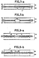
- Figures 7, a and b show two variants of the device according to the invention, each carrying two semiconductor washers.
- FIG. 7a two devices have been shown for example as described in FIG. 1a, marked 91 and 92 and placed so that their bottom 4 is in contact with one another.
- the connection pads of each box to the outside, marked respectively 93 and 94, are placed on the outer (upper) face of these.
- the covers have been shown apart, for clarity of the drawing.
- the two casings concerned are of the type of that of FIG. 4, which makes it possible to use only one central pillar for the assembly, marked 95.
- the connection pads of each box to the outside are placed on the outside faces of the boxes 96 and 97.
- FIGS. 8, a and b represent the application of the box according to the invention to the encapsulation of a hybrid circuit.
- the box is shown in its embodiment of FIG. 1.
- FIG. 8a we therefore find the housing according to the invention as shown in FIG. 1a, that is to say comprising a bottom 4 fixed to a peripheral ring 2 and to a central pillar 5, the whole being closed by a cover 3.
- the washer 1 of semiconductor material is replaced by a hybrid circuit, generally identified 75 and comprising components 77, passive or active discrete circuits and integrated circuits, arranged on an insulating substrate 76.
- the peripheral ring 2 is inserted for example in two connectors 9, U-shaped, similar to those of FIGS. 6.
- FIG. 8b is shown, seen from above, an alternative embodiment in which the substrate 76 of the hybrid circuit 75 is divided into a certain number of parts, for example four, marked 76-1, 76-2, 76-3 and 76-4.
- some components 77 have been shown diagrammatically.
- the bottom 4 of the housing projects outside as illustrated in FIG. 6b, for the same reasons.
- the power supplies, received by the box on the connectors 9, are transmitted to the hybrid circuit either by its peripheral pads, marked 73, or by its central pads, marked 74, via conductive planes arranged, as previously, in the bottom 4 or in cover 3.
- the supply of the power supply is done by conducting planes at a certain number of points distributed over the surface of the hybrid circuit 75 (in the center in the example of FIGS. 8, but which can be distributed differently, as illustrated in FIGS. 5 for example), and not as previously by wire to the periphery of the substrate of the hybrid circuit then by conductive track deposited on the substrate until to the component to be supplied.
- Figures 9 a and b show two alternative embodiments, seen in section, of the encapsulation according to the invention of two hybrid circuits.
- FIG. 9a there are two housings, for example as described in FIG. 8a, marked respectively 78 and 79, fixed to each other by their bottom 8.
- FIG. 9b represents another variant, in which the insulating substrate of the hybrid circuit, marked 76, carries both the peripheral ring 2 and the central pillar 5 of the housing, the latter comprising as above a cover 3.
- the insulating substrate of the hybrid circuit marked 76
- carries both the peripheral ring 2 and the central pillar 5 of the housing the latter comprising as above a cover 3.
- two such boxes have been placed, marked 88 and 89, fixed respectively on each of the faces of a heat sink marked 85.
- the assembly forms a rigid block that can be electrically connected at its ends, for example by U-shaped connectors as described in the previous figure.
- conducting supply supply planes can be placed both in the base and the housing cover.
Landscapes
- Engineering & Computer Science (AREA)
- Microelectronics & Electronic Packaging (AREA)
- Power Engineering (AREA)
- Physics & Mathematics (AREA)
- Condensed Matter Physics & Semiconductors (AREA)
- General Physics & Mathematics (AREA)
- Computer Hardware Design (AREA)
- Semiconductor Integrated Circuits (AREA)
- Casings For Electric Apparatus (AREA)
- Testing Or Measuring Of Semiconductors Or The Like (AREA)
Claims (11)
Applications Claiming Priority (2)
| Application Number | Priority Date | Filing Date | Title |
|---|---|---|---|
| FR8518695A FR2591801B1 (fr) | 1985-12-17 | 1985-12-17 | Boitier d'encapsulation d'un circuit electronique |
| FR8518695 | 1985-12-17 |
Publications (2)
| Publication Number | Publication Date |
|---|---|
| EP0228953A1 EP0228953A1 (de) | 1987-07-15 |
| EP0228953B1 true EP0228953B1 (de) | 1990-10-10 |
Family
ID=9325888
Family Applications (1)
| Application Number | Title | Priority Date | Filing Date |
|---|---|---|---|
| EP86402788A Expired - Lifetime EP0228953B1 (de) | 1985-12-17 | 1986-12-12 | Verkapselungsgehäuse für eine elektronische Schaltung |
Country Status (4)
| Country | Link |
|---|---|
| US (1) | US4755910A (de) |
| EP (1) | EP0228953B1 (de) |
| DE (1) | DE3674905D1 (de) |
| FR (1) | FR2591801B1 (de) |
Families Citing this family (38)
| Publication number | Priority date | Publication date | Assignee | Title |
|---|---|---|---|---|
| US5007841A (en) * | 1983-05-31 | 1991-04-16 | Trw Inc. | Integrated-circuit chip interconnection system |
| FR2618255A1 (fr) * | 1987-07-14 | 1989-01-20 | Gen Electric | Bloc de conditionnement pour le montage et l'interconnexion de puces semiconductrices. |
| FR2621173B1 (fr) * | 1987-09-29 | 1989-12-08 | Bull Sa | Boitier pour circuit integre de haute densite |
| FR2623662B1 (fr) * | 1987-11-20 | 1990-03-09 | Labo Electronique Physique | Dispositif de connexion pour circuits integres numeriques ultra-rapides |
| US5223741A (en) * | 1989-09-01 | 1993-06-29 | Tactical Fabs, Inc. | Package for an integrated circuit structure |
| FR2663159B1 (fr) * | 1990-06-12 | 1997-01-24 | Thomson Hybrides | Systeme de conditionnement hermetique d'un module hybride. |
| US5241456A (en) * | 1990-07-02 | 1993-08-31 | General Electric Company | Compact high density interconnect structure |
| US5147985A (en) * | 1990-08-14 | 1992-09-15 | The Scabbard Corporation | Sheet batteries as substrate for electronic circuit |
| US5124508A (en) * | 1990-08-14 | 1992-06-23 | The Scabbard Corp. | Application of sheet batteries as support base for electronic circuits |
| DE4031733A1 (de) * | 1990-10-06 | 1992-04-09 | Bosch Gmbh Robert | Mehrlagenhybride mit leistungsbauelementen |
| US5138436A (en) * | 1990-11-16 | 1992-08-11 | Ball Corporation | Interconnect package having means for waveguide transmission of rf signals |
| JPH05152509A (ja) * | 1991-11-27 | 1993-06-18 | Hitachi Ltd | 電子回路システム装置 |
| FR2688629A1 (fr) * | 1992-03-10 | 1993-09-17 | Thomson Csf | Procede et dispositif d'encapsulation en trois dimensions de pastilles semi-conductrices. |
| FR2706222B1 (fr) * | 1993-06-08 | 1995-07-13 | Alcatel Espace | Assemblage haute densité, haute fiabilité de circuits intégrés et son procédé de réalisation. |
| US5313363A (en) * | 1993-07-28 | 1994-05-17 | Eml Research, Inc. | Low impedance interconnection assembly for high frequency switching power semiconductor devices and low inductance modular capacitor |
| US5388028A (en) * | 1993-07-28 | 1995-02-07 | Kaman Electromagnetics Corporation | Low impedance interconnection assembly for high frequency switching power semiconductor devices and low inductance modular capacitor |
| FR2709020B1 (fr) * | 1993-08-13 | 1995-09-08 | Thomson Csf | Procédé d'interconnexion de pastilles semi-conductrices en trois dimensions, et composant en résultant. |
| FR2719967B1 (fr) * | 1994-05-10 | 1996-06-07 | Thomson Csf | Interconnexion en trois dimensions de boîtiers de composants électroniques utilisant des circuits imprimés. |
| DE4421319A1 (de) * | 1994-06-17 | 1995-12-21 | Abb Management Ag | Niederinduktives Leistungshalbleitermodul |
| US6954368B1 (en) | 1996-07-22 | 2005-10-11 | HYDRO-QUéBEC | Low stray interconnection inductance power converting molecule for converting a DC voltage into an AC voltage, and a method therefor |
| US6125039A (en) * | 1996-07-31 | 2000-09-26 | Taiyo Yuden Co., Ltd. | Hybrid module |
| US7321485B2 (en) | 1997-04-08 | 2008-01-22 | X2Y Attenuators, Llc | Arrangement for energy conditioning |
| US7336468B2 (en) | 1997-04-08 | 2008-02-26 | X2Y Attenuators, Llc | Arrangement for energy conditioning |
| US9054094B2 (en) | 1997-04-08 | 2015-06-09 | X2Y Attenuators, Llc | Energy conditioning circuit arrangement for integrated circuit |
| US6535398B1 (en) | 2000-03-07 | 2003-03-18 | Fujitsu Limited | Multichip module substrates with buried discrete capacitors and components and methods for making |
| FR2832136B1 (fr) * | 2001-11-09 | 2005-02-18 | 3D Plus Sa | Dispositif d'encapsulation hermetique de composant devant etre protege de toute contrainte |
| FR2857157B1 (fr) * | 2003-07-01 | 2005-09-23 | 3D Plus Sa | Procede d'interconnexion de composants actif et passif et composant heterogene a faible epaisseur en resultant |
| FR2875672B1 (fr) * | 2004-09-21 | 2007-05-11 | 3D Plus Sa Sa | Dispositif electronique avec repartiteur de chaleur integre |
| US7630188B2 (en) | 2005-03-01 | 2009-12-08 | X2Y Attenuators, Llc | Conditioner with coplanar conductors |
| FR2884049B1 (fr) * | 2005-04-01 | 2007-06-22 | 3D Plus Sa Sa | Module electronique de faible epaisseur comprenant un empilement de boitiers electroniques a billes de connexion |
| FR2894070B1 (fr) * | 2005-11-30 | 2008-04-11 | 3D Plus Sa Sa | Module electronique 3d |
| FR2895568B1 (fr) * | 2005-12-23 | 2008-02-08 | 3D Plus Sa Sa | Procede de fabrication collective de modules electroniques 3d |
| FR2905198B1 (fr) * | 2006-08-22 | 2008-10-17 | 3D Plus Sa Sa | Procede de fabrication collective de modules electroniques 3d |
| FR2911995B1 (fr) * | 2007-01-30 | 2009-03-06 | 3D Plus Sa Sa | Procede d'interconnexion de tranches electroniques |
| US7919839B2 (en) * | 2007-07-24 | 2011-04-05 | Northrop Grumman Systems Corporation | Support structures for on-wafer testing of wafer-level packages and multiple wafer stacked structures |
| FR2923081B1 (fr) * | 2007-10-26 | 2009-12-11 | 3D Plus | Procede d'interconnexion verticale de modules electroniques 3d par des vias. |
| FR2940521B1 (fr) | 2008-12-19 | 2011-11-11 | 3D Plus | Procede de fabrication collective de modules electroniques pour montage en surface |
| FR2943176B1 (fr) | 2009-03-10 | 2011-08-05 | 3D Plus | Procede de positionnement des puces lors de la fabrication d'une plaque reconstituee |
Family Cites Families (19)
| Publication number | Priority date | Publication date | Assignee | Title |
|---|---|---|---|---|
| FR2456388A1 (fr) * | 1979-05-10 | 1980-12-05 | Thomson Brandt | Microboitier de circuit electronique, et circuit hybride comportant un tel microboitier |
| US4288841A (en) * | 1979-09-20 | 1981-09-08 | Bell Telephone Laboratories, Incorporated | Double cavity semiconductor chip carrier |
| US4320438A (en) * | 1980-05-15 | 1982-03-16 | Cts Corporation | Multi-layer ceramic package |
| FR2485262A1 (fr) * | 1980-06-19 | 1981-12-24 | Thomson Csf | Boitier d'encapsulation resistant a de fortes pressions externes |
| FR2485796A1 (fr) * | 1980-06-24 | 1981-12-31 | Thomson Csf | Resistance electrique chauffante et tete d'imprimante thermique comportant de telles resistances chauffantes |
| US4328530A (en) * | 1980-06-30 | 1982-05-04 | International Business Machines Corporation | Multiple layer, ceramic carrier for high switching speed VLSI chips |
| JPS57207356A (en) * | 1981-06-15 | 1982-12-20 | Fujitsu Ltd | Semiconductor device |
| JPS5896757A (ja) * | 1981-12-04 | 1983-06-08 | Hitachi Ltd | 半導体装置 |
| FR2525815B1 (fr) * | 1982-04-27 | 1985-08-30 | Inf Milit Spatiale Aeronaut | Substrat composite a haute conduction thermique et application aux boitiers de dispositifs semi-conducteurs |
| FR2527039A1 (fr) * | 1982-05-14 | 1983-11-18 | Inf Milit Spatiale Aeronaut | Dispositif de protection d'un dispositif electronique contre les tensions engendrees par un champ electromagnetique |
| FR2538618B1 (fr) * | 1982-12-28 | 1986-03-07 | Inf Milit Spatiale Aeronaut | Boitier pour composant electronique comportant un element fixant l'humidite |
| US4563725A (en) * | 1983-01-06 | 1986-01-07 | Welwyn Electronics Limited | Electrical assembly |
| US4628407A (en) * | 1983-04-22 | 1986-12-09 | Cray Research, Inc. | Circuit module with enhanced heat transfer and distribution |
| FR2547113B1 (fr) * | 1983-06-03 | 1986-11-07 | Inf Milit Spatiale Aeronaut | Boitier d'encapsulation de composant electronique, durci vis-a-vis des radiations |
| FR2550009B1 (fr) * | 1983-07-29 | 1986-01-24 | Inf Milit Spatiale Aeronaut | Boitier de composant electronique muni d'un condensateur |
| US4612601A (en) * | 1983-11-30 | 1986-09-16 | Nec Corporation | Heat dissipative integrated circuit chip package |
| US4614194A (en) * | 1984-01-20 | 1986-09-30 | Cordis Corporation | Implantable pulse generator having a single printed circuit board for carrying integrated circuit chips thereon with chip carrier means |
| JPS60192359A (ja) * | 1984-03-14 | 1985-09-30 | Nec Corp | 半導体メモリ装置 |
| FR2565032B1 (fr) * | 1984-05-25 | 1987-02-20 | Inf Milit Spatiale Aeronaut | Dispositif de repartition de potentiel electrique et boitier de composant electronique incorporant un tel dispositif |
-
1985
- 1985-12-17 FR FR8518695A patent/FR2591801B1/fr not_active Expired
-
1986
- 1986-12-12 EP EP86402788A patent/EP0228953B1/de not_active Expired - Lifetime
- 1986-12-12 DE DE8686402788T patent/DE3674905D1/de not_active Expired - Fee Related
- 1986-12-17 US US06/942,655 patent/US4755910A/en not_active Expired - Fee Related
Also Published As
| Publication number | Publication date |
|---|---|
| US4755910A (en) | 1988-07-05 |
| EP0228953A1 (de) | 1987-07-15 |
| DE3674905D1 (de) | 1990-11-15 |
| FR2591801B1 (fr) | 1988-10-14 |
| FR2591801A1 (fr) | 1987-06-19 |
Similar Documents
| Publication | Publication Date | Title |
|---|---|---|
| EP0228953B1 (de) | Verkapselungsgehäuse für eine elektronische Schaltung | |
| EP0133125B1 (de) | Gehäuse für einen elektronischen Baustein mit einem Kondensator | |
| EP0108098A1 (de) | Schutzelemente für elektronische bauteile gegen spannungen verursacht durch ein elektromagnetisches feld | |
| EP0310463A1 (de) | Gehäuse für einen hochintegrierten Schaltkreis | |
| FR2700416A1 (fr) | Dispositif à semiconducteurs comportant un élément semiconducteur sur un élément de montage. | |
| FR2518811A1 (fr) | Dispositif a circuit integre en conteneur de ceramique | |
| FR2606206A1 (fr) | Condensateur de decouplage pour module a reseau d'ergots en grille | |
| FR2529013A1 (fr) | Circuit a haute frequence et dispositif semi-conducteur pour equiper un tel circuit | |
| EP0490739A1 (de) | Verfahren und Anordnung zum Verbinden integrierter Schaltungen in drei Dimensionen | |
| FR2645681A1 (fr) | Dispositif d'interconnexion verticale de pastilles de circuits integres et son procede de fabrication | |
| EP0166634B1 (de) | Einrichtung zur Verteilung von elektrischen Potentialen, und eine solche Einrichtung enthaltendes Gehäuse für elektronische Komponenten | |
| EP1657749B1 (de) | Mehrlagiges Mikroelektronik-Gehäuse mit interner Abschirmung | |
| EP0346206A1 (de) | Aktiver Verbinder für Leiterplatten | |
| FR2629271A1 (fr) | Dispositif d'interconnexion et de protection d'une pastille nue de composant hyperfrequence | |
| FR2565030A1 (fr) | Structure de metallisations de reprise de contacts d'un dispositif semi-conducteur et dispositif dote d'une telle structure | |
| EP0079265A1 (de) | Verfahren zum Herstellen eines Sockels zum Montieren eines Halbleiterchips auf die Basis eines Verkapselungsgehäuses | |
| FR2495837A1 (fr) | Embase de microboitier d'encapsulation et microboitier comportant une telle embase | |
| FR2620275A1 (fr) | Boitier pour le montage en surface d'un composant fonctionnant en hyperfrequences | |
| FR2489592A1 (fr) | Micro-boitier ceramique d'encapsulation de circuit electronique | |
| FR2535110A1 (fr) | Procede d'encapsulation d'un composant semi-conducteur dans un circuit electronique realise sur substrat et application aux circuits integres rapides | |
| FR2529386A1 (fr) | Boitier de circuit electronique comportant un condensateur | |
| EP0030168B1 (de) | Vorrichtung zur Parallelschaltung von Höchstfrequenz-Leistungstransistoren | |
| EP0101335A1 (de) | Mikrogehaüse-Verkapselung für logische integrierte Schaltungen, funktionierend bei sehr hoher Frequenz | |
| FR2726941A1 (fr) | Dispositif integre de protection par varistance d'un composant electronique contre les effets d'un champ electro-magnetique ou de charges statiques | |
| EP0282396A1 (de) | Komplexe Hybridschaltungsstruktur und Verfahren zur Herstellung |
Legal Events
| Date | Code | Title | Description |
|---|---|---|---|
| PUAI | Public reference made under article 153(3) epc to a published international application that has entered the european phase |
Free format text: ORIGINAL CODE: 0009012 |
|
| AK | Designated contracting states |
Kind code of ref document: A1 Designated state(s): DE GB IT NL |
|
| 17P | Request for examination filed |
Effective date: 19871221 |
|
| 17Q | First examination report despatched |
Effective date: 19900227 |
|
| RAP1 | Party data changed (applicant data changed or rights of an application transferred) |
Owner name: THOMSON-CSF |
|
| RAP1 | Party data changed (applicant data changed or rights of an application transferred) |
Owner name: THOMSON-CSF |
|
| GRAA | (expected) grant |
Free format text: ORIGINAL CODE: 0009210 |
|
| AK | Designated contracting states |
Kind code of ref document: B1 Designated state(s): DE GB IT NL |
|
| ITF | It: translation for a ep patent filed | ||
| REF | Corresponds to: |
Ref document number: 3674905 Country of ref document: DE Date of ref document: 19901115 |
|
| GBT | Gb: translation of ep patent filed (gb section 77(6)(a)/1977) | ||
| PLBE | No opposition filed within time limit |
Free format text: ORIGINAL CODE: 0009261 |
|
| STAA | Information on the status of an ep patent application or granted ep patent |
Free format text: STATUS: NO OPPOSITION FILED WITHIN TIME LIMIT |
|
| 26N | No opposition filed | ||
| ITTA | It: last paid annual fee | ||
| PGFP | Annual fee paid to national office [announced via postgrant information from national office to epo] |
Ref country code: DE Payment date: 19921112 Year of fee payment: 7 |
|
| PGFP | Annual fee paid to national office [announced via postgrant information from national office to epo] |
Ref country code: GB Payment date: 19921118 Year of fee payment: 7 |
|
| PGFP | Annual fee paid to national office [announced via postgrant information from national office to epo] |
Ref country code: NL Payment date: 19921231 Year of fee payment: 7 |
|
| PG25 | Lapsed in a contracting state [announced via postgrant information from national office to epo] |
Ref country code: GB Effective date: 19931212 |
|
| PG25 | Lapsed in a contracting state [announced via postgrant information from national office to epo] |
Ref country code: NL Effective date: 19940701 |
|
| GBPC | Gb: european patent ceased through non-payment of renewal fee |
Effective date: 19931212 |
|
| NLV4 | Nl: lapsed or anulled due to non-payment of the annual fee | ||
| PG25 | Lapsed in a contracting state [announced via postgrant information from national office to epo] |
Ref country code: DE Effective date: 19940901 |
|
| PG25 | Lapsed in a contracting state [announced via postgrant information from national office to epo] |
Ref country code: IT Free format text: LAPSE BECAUSE OF NON-PAYMENT OF DUE FEES;WARNING: LAPSES OF ITALIAN PATENTS WITH EFFECTIVE DATE BEFORE 2007 MAY HAVE OCCURRED AT ANY TIME BEFORE 2007. THE CORRECT EFFECTIVE DATE MAY BE DIFFERENT FROM THE ONE RECORDED. Effective date: 20051212 |