EP0228317B1 - Elektrooptischer Anzeigeschirm mit Steuertransistoren - Google Patents
Elektrooptischer Anzeigeschirm mit Steuertransistoren Download PDFInfo
- Publication number
- EP0228317B1 EP0228317B1 EP86402508A EP86402508A EP0228317B1 EP 0228317 B1 EP0228317 B1 EP 0228317B1 EP 86402508 A EP86402508 A EP 86402508A EP 86402508 A EP86402508 A EP 86402508A EP 0228317 B1 EP0228317 B1 EP 0228317B1
- Authority
- EP
- European Patent Office
- Prior art keywords
- line
- electro
- control
- conductor
- connection
- Prior art date
- Legal status (The legal status is an assumption and is not a legal conclusion. Google has not performed a legal analysis and makes no representation as to the accuracy of the status listed.)
- Expired - Lifetime
Links
- 239000004020 conductor Substances 0.000 claims description 129
- 239000011159 matrix material Substances 0.000 claims description 29
- 239000000463 material Substances 0.000 claims description 13
- 238000003860 storage Methods 0.000 claims description 9
- 239000003990 capacitor Substances 0.000 claims description 8
- 239000004065 semiconductor Substances 0.000 claims description 6
- 239000011810 insulating material Substances 0.000 claims description 3
- 239000004973 liquid crystal related substance Substances 0.000 description 32
- PEDCQBHIVMGVHV-UHFFFAOYSA-N Glycerine Chemical compound OCC(O)CO PEDCQBHIVMGVHV-UHFFFAOYSA-N 0.000 description 16
- 210000004027 cell Anatomy 0.000 description 15
- 210000002858 crystal cell Anatomy 0.000 description 11
- 238000010586 diagram Methods 0.000 description 10
- 101710114762 50S ribosomal protein L11, chloroplastic Proteins 0.000 description 6
- 238000004519 manufacturing process Methods 0.000 description 6
- 239000011521 glass Substances 0.000 description 4
- 239000010409 thin film Substances 0.000 description 3
- 238000012800 visualization Methods 0.000 description 3
- 238000012550 audit Methods 0.000 description 2
- 230000008878 coupling Effects 0.000 description 2
- 238000010168 coupling process Methods 0.000 description 2
- 238000005859 coupling reaction Methods 0.000 description 2
- 230000000694 effects Effects 0.000 description 2
- 230000006870 function Effects 0.000 description 2
- 101710082414 50S ribosomal protein L12, chloroplastic Proteins 0.000 description 1
- 229910021417 amorphous silicon Inorganic materials 0.000 description 1
- 238000013459 approach Methods 0.000 description 1
- 230000007547 defect Effects 0.000 description 1
- 230000002950 deficient Effects 0.000 description 1
- 238000000151 deposition Methods 0.000 description 1
- 238000013461 design Methods 0.000 description 1
- 238000009826 distribution Methods 0.000 description 1
- 230000005684 electric field Effects 0.000 description 1
- 238000009434 installation Methods 0.000 description 1
- 239000012212 insulator Substances 0.000 description 1
- 230000010354 integration Effects 0.000 description 1
- 230000003446 memory effect Effects 0.000 description 1
- 239000002184 metal Substances 0.000 description 1
- 238000000034 method Methods 0.000 description 1
- 238000009877 rendering Methods 0.000 description 1
- 238000012546 transfer Methods 0.000 description 1
Images


Classifications
-
- H—ELECTRICITY
- H04—ELECTRIC COMMUNICATION TECHNIQUE
- H04N—PICTORIAL COMMUNICATION, e.g. TELEVISION
- H04N3/00—Scanning details of television systems; Combination thereof with generation of supply voltages
- H04N3/10—Scanning details of television systems; Combination thereof with generation of supply voltages by means not exclusively optical-mechanical
- H04N3/12—Scanning details of television systems; Combination thereof with generation of supply voltages by means not exclusively optical-mechanical by switched stationary formation of lamps, photocells or light relays
- H04N3/127—Scanning details of television systems; Combination thereof with generation of supply voltages by means not exclusively optical-mechanical by switched stationary formation of lamps, photocells or light relays using liquid crystals
-
- G—PHYSICS
- G02—OPTICS
- G02F—OPTICAL DEVICES OR ARRANGEMENTS FOR THE CONTROL OF LIGHT BY MODIFICATION OF THE OPTICAL PROPERTIES OF THE MEDIA OF THE ELEMENTS INVOLVED THEREIN; NON-LINEAR OPTICS; FREQUENCY-CHANGING OF LIGHT; OPTICAL LOGIC ELEMENTS; OPTICAL ANALOGUE/DIGITAL CONVERTERS
- G02F1/00—Devices or arrangements for the control of the intensity, colour, phase, polarisation or direction of light arriving from an independent light source, e.g. switching, gating or modulating; Non-linear optics
- G02F1/01—Devices or arrangements for the control of the intensity, colour, phase, polarisation or direction of light arriving from an independent light source, e.g. switching, gating or modulating; Non-linear optics for the control of the intensity, phase, polarisation or colour
- G02F1/13—Devices or arrangements for the control of the intensity, colour, phase, polarisation or direction of light arriving from an independent light source, e.g. switching, gating or modulating; Non-linear optics for the control of the intensity, phase, polarisation or colour based on liquid crystals, e.g. single liquid crystal display cells
- G02F1/133—Constructional arrangements; Operation of liquid crystal cells; Circuit arrangements
- G02F1/136—Liquid crystal cells structurally associated with a semi-conducting layer or substrate, e.g. cells forming part of an integrated circuit
- G02F1/1362—Active matrix addressed cells
- G02F1/1368—Active matrix addressed cells in which the switching element is a three-electrode device
-
- G—PHYSICS
- G09—EDUCATION; CRYPTOGRAPHY; DISPLAY; ADVERTISING; SEALS
- G09G—ARRANGEMENTS OR CIRCUITS FOR CONTROL OF INDICATING DEVICES USING STATIC MEANS TO PRESENT VARIABLE INFORMATION
- G09G3/00—Control arrangements or circuits, of interest only in connection with visual indicators other than cathode-ray tubes
- G09G3/20—Control arrangements or circuits, of interest only in connection with visual indicators other than cathode-ray tubes for presentation of an assembly of a number of characters, e.g. a page, by composing the assembly by combination of individual elements arranged in a matrix no fixed position being assigned to or needed to be assigned to the individual characters or partial characters
- G09G3/34—Control arrangements or circuits, of interest only in connection with visual indicators other than cathode-ray tubes for presentation of an assembly of a number of characters, e.g. a page, by composing the assembly by combination of individual elements arranged in a matrix no fixed position being assigned to or needed to be assigned to the individual characters or partial characters by control of light from an independent source
- G09G3/36—Control arrangements or circuits, of interest only in connection with visual indicators other than cathode-ray tubes for presentation of an assembly of a number of characters, e.g. a page, by composing the assembly by combination of individual elements arranged in a matrix no fixed position being assigned to or needed to be assigned to the individual characters or partial characters by control of light from an independent source using liquid crystals
- G09G3/3611—Control of matrices with row and column drivers
- G09G3/3648—Control of matrices with row and column drivers using an active matrix
-
- G—PHYSICS
- G02—OPTICS
- G02F—OPTICAL DEVICES OR ARRANGEMENTS FOR THE CONTROL OF LIGHT BY MODIFICATION OF THE OPTICAL PROPERTIES OF THE MEDIA OF THE ELEMENTS INVOLVED THEREIN; NON-LINEAR OPTICS; FREQUENCY-CHANGING OF LIGHT; OPTICAL LOGIC ELEMENTS; OPTICAL ANALOGUE/DIGITAL CONVERTERS
- G02F1/00—Devices or arrangements for the control of the intensity, colour, phase, polarisation or direction of light arriving from an independent light source, e.g. switching, gating or modulating; Non-linear optics
- G02F1/01—Devices or arrangements for the control of the intensity, colour, phase, polarisation or direction of light arriving from an independent light source, e.g. switching, gating or modulating; Non-linear optics for the control of the intensity, phase, polarisation or colour
- G02F1/13—Devices or arrangements for the control of the intensity, colour, phase, polarisation or direction of light arriving from an independent light source, e.g. switching, gating or modulating; Non-linear optics for the control of the intensity, phase, polarisation or colour based on liquid crystals, e.g. single liquid crystal display cells
- G02F1/133—Constructional arrangements; Operation of liquid crystal cells; Circuit arrangements
- G02F1/136—Liquid crystal cells structurally associated with a semi-conducting layer or substrate, e.g. cells forming part of an integrated circuit
- G02F1/1362—Active matrix addressed cells
- G02F1/136213—Storage capacitors associated with the pixel electrode
-
- G—PHYSICS
- G02—OPTICS
- G02F—OPTICAL DEVICES OR ARRANGEMENTS FOR THE CONTROL OF LIGHT BY MODIFICATION OF THE OPTICAL PROPERTIES OF THE MEDIA OF THE ELEMENTS INVOLVED THEREIN; NON-LINEAR OPTICS; FREQUENCY-CHANGING OF LIGHT; OPTICAL LOGIC ELEMENTS; OPTICAL ANALOGUE/DIGITAL CONVERTERS
- G02F2201/00—Constructional arrangements not provided for in groups G02F1/00 - G02F7/00
- G02F2201/12—Constructional arrangements not provided for in groups G02F1/00 - G02F7/00 electrode
- G02F2201/122—Constructional arrangements not provided for in groups G02F1/00 - G02F7/00 electrode having a particular pattern
Definitions
- the invention relates to an electrooptical display screen with control transistors and more particularly a flat screen in which the control of each picture element to be displayed is done using a control transistor. It is applicable to the production of large liquid crystal flat screens whose control points are made by integration in the form of thin layers.
- these screens generally comprise a large number of elementary points or picture elements of square or rectangular shape. These picture elements must be addressed individually. The definition of the screen depends on the number of points likely to receive information. The control of each point is done by application of an electric field through the liquid crystal. For the display of alphanumeric or graphic information, matrix type displays have been proposed. Each picture element is then defined by the intersection of two networks of orthogonal conductors called rows and columns.
- a now usual way of solving this problem consists in carrying out this addressing using a matrix of thin film transistors: this amounts to directly coupling the electrooptic effect on a giant but low resolution "integrated circuit" charged with '' provide information referral and storage functions.
- the transistors are located at the crossing points of line conductors and column conductors isolated from each other, so that an appropriate potential difference applied between a line and a column determines the conduction of the transistor connected between this line and this column.
- the invention therefore relates to an arrangement which makes it possible to overcome these drawbacks by simplifying the structure of the addressing matrices with thin film transistors.
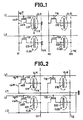
- a liquid crystal screen essentially comprises two glass plates enclosing a liquid crystal. The internal faces of these plates, in contact with the liquid crystal, carry the circuits of the liquid crystal screen.
- the screen control matrix is located on one of its faces. As shown in FIG. 1, it comprises row conductors L1 and L2 and column conductors K1 and K2. The row and column conductors cross without any connection between them. At each crossing between a row conductor and a column conductor is connected a transistor having its gate connected to a line and its source to a column. Thus, at the intersection of line L1 and column K1 is connected a transistor T11 having a gate connected by a gate connection cg 11 to line L1 and a source connected by a source connection cs11 to column K1.
- columns K1, K2 and transistors T11 are implanted metal electrodes at the intersection of each line and each column. Each of these electrodes is connected to the drain of a previously described transistor. Thus, at the crossing of the line L1 and the column K1, an electrode E11 is connected by a drain connection cd11 to the drain of the transistor T11.
- each electrode such as E11 is an electrode.
- This electrode is connected to ground.
- all the electrodes of this face being connected to ground, consist of a single ground plate.
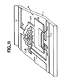
- FIG. 3 Such a screen configuration is shown in perspective in FIG. 3.
- the row conductors L1 and L2 the column conductors K1, K2 and K3.
- transistors and electrodes such as the transistor T11 and the electrode E11 situated at the crossing of the row conductor L1 and the column conductor K1.
- a second blade 2 determines with one of these faces 20 and the face 10 of the blade 1, a space 3 in which a liquid crystal is placed.
- the face 20 also has a transparent ground plate.
- a face 10 electrode such as E11, the facing earth plate and the liquid crystal which separate them constitute a liquid crystal cell CL11 of the screen.
- FIG. 2 shows the network of line conductors L1 and L2, the matrix of transistors T11, T12, T21, T22 and the matrix of electrodes E11, E12, E21, E22.
- a second network of line conductors L'1, L'2 is arranged parallel to the line conductors L1, L2.
- the source connections then connect the sources of the transistors to these line conductors L'1 and L'2.
- the transistor T11 has its gate connected to the line conductor L1, its source connected to the line conductor L'1, its drain connected to the electrode E11.
- the electrodes F11 to F22 are connected to column conductors C1, C2.
- the line conductors L'1 and L'2 are connected to a reference potential such as ground.
- the operation of this screen and the control of a liquid crystal cell CL1 1 is done by application of appropriate potentials on the line conductors, such as L1, and the column conductors such as C1.
- FIGS. 4 and 5 a crossing point of the type of screen in FIG. 1 has been shown.
- a storage capacitor CK11 has been connected between the drain of the transistor T11 and the line conductor L1. It is possible, as shown in FIG. 5, to connect a storage capacitor CK11 between the drain of the transistor T11 and a neighboring line conductor L2.
- the manufacture of a screen of known type requires the installation on the same face of the liquid crystal screen, that is to say networks of conductors which cross but isolated from each other. others, or two networks of line conductors.
- the invention relates to a simpler structure display screen therefore easier to produce and less susceptible to manufacturing defects, therefore more reliable.
- This screen comprises two glass blades 1 and 2 arranged in parallel. Between these two glass blades 1 and 2 is placed an electrooptical material 3 in contact with the faces 10 and 20 of these blades.
- a matrix of electrodes E11 to E23 arranged in rows and columns. Parallel to the electrode lines are arranged line conductors L1 to L3.
- Each electrode is associated with a transistor T11 1 to T33.
- the gate of each of the transistors of a line is connected to an associated line conductor.
- the source of these transistors is connected to a neighboring line conductor.
- the drain of each transistor is connected to the electrode associated with the transistor.
- the gate of transistor T11 is connected by a gate connection cg11 to a line conductor L1, that the source of this transistor is connected by a source connection cs11 to the next line conductor L2 and that the drain is connected to an electrode E11 by a drain connection cd 11.
- the face 20 of the blade 2 carries electrodes located opposite the electrodes E11 to E23.
- an electrode such as F11, opposite each electrode E11 to E23.
- a pair of electrodes such as E11 - F11 and the liquid crystal situated between these electrodes constitutes a liquid crystal cell CL11.
- the electrodes of the face 20 constituting the same column are connected to a column conductor C1, C2.
- the electrodes of the face 20 are produced in the form of elongated electrodes C1, C2 each corresponding to a column of electrodes of the face 10. Each electrode C1, C2 therefore also acts as a column conductor.
- the control of a cell, CL11 for example is done by application of a gate control potential Vg on a line, L1 according to the example then, of a source supply potential Vs on the row line next, so line L2 according to the same example. Furthermore, a drain potential is applied to the column conductor (or column electrode) C1.
- the operation of a cell implies that the control of a line of cells prevents the control of the lines of neighboring cells due to the fact that the different transistors are connected between two line conductors. This requires a sequential operation of the screen of the invention, that is to say a sequential control of the different lines of the screen.
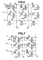
- a screen comprising a matrix of m x n cells arranged in m rows and n columns. These cells are associated with m ⁇ n transistors T11 to Tmn.
- Three generators Gg, Gs and Gd respectively provide gate, threshold and drain potentials suitable for the conduction of the transistors.
- the generators Gg and Gs are connectable to the line conductors L1 to Lm by connection circuits AL1 to ALm.
- a connection circuit AL1 to ALm connects the generator Gg to the corresponding line conductor when it receives a level 1 control signal on its input d1.
- a Dm distributor provides a level 1 signal on a single output d1 to dm. It supplies this signal successively on all outputs d1 to dm. When it provides a level 1 signal on one output, it provides a level O signal on all other outputs.
- a single connection circuit AL1 to ALm at a time therefore connects the generator Gg to a line conductor while the other connection circuits connect the generator Gs to the other line conductors.
- a generator Gd enables the column conductors to be supplied simultaneously at different voltage levels, thus determining the control of transistors and associated cells under different voltage levels.
- the circuit of FIG. 9 thus makes it possible to carry out a sequential control line by line of the screen.
- the distributor Dm provides a level 1 signal on its output d1 and a level 0 signal on all its other outputs
- only the connection circuit A11 connects the generator Gg to the line conductor L1, the other connection circuits , and in particular AL2, connect the generator Gs to the other line conductors L2 to Lm.
- Line conductor L1 is at potential Vg and the other line conductors are all at potential Vs.
- the distributor Dn supplies each column conductor with a specific control potential supplied by the generator Gd.
- the cells of line L1 are thus each controlled under a particular voltage level.
- the transistors T1 and T12 located at the crossing points of the line conductor L1 and of the column conductors C1 and C2 controlled are made conductive and the associated cells CL11 and CL12 change state.
- the distributor Dm then supplies a level 1 signal on the output d2.
- the connection circuit AL2 connects the generator Gg to the line conductor L2, while the generator Gs is connected to the other line conductors.
- the distributor Dn connects the generator Gd to the appropriate column conductors C1 to Cn determining the control of cells connected to the line conductor L2.
- connection commands to the connection circuits AL1 to ALm can be carried out simply, as shown in FIG. 10, using a shift register REG.
- This register REG comprises as many stages A1 to Am as there are line conductors. It is supplied by a generator Gg providing a gate potential Vg and a generator Gs providing a threshold potential Vs.
- a line conductor L1 to Lm is connected to each stage A1 to Am.
- a stage When a stage is at state 0, it provides a source potential Vs on the line conductor which is connected to it.
- a stage When a stage is in state 1, it provides a gate potential on the line conductor.
- a control circuit DEC supplies a signal of logic level 1 to an input of the first stage and controls its shift in the successive stages of the register, controlling the supply of the potential Vg on the successive line conductors L1 to Lm, a single conductor of line at a time being at the potential Vg while the others are at the potential Vs.
- the supply by the generator Gd and the distributor Dn, of the column conductors C1 to Cn is carried out as described with reference to FIG. 9. thus a sequential command line by line of the screen.
- the sources of the transistors of a line of the screen matrix instead of being connected to the line conductor of the next rank, are connected to the same line conductor as the gates of the same transistors .
- a crossing point according to the invention and its transistor such as T11 can be produced as shown by way of example in FIG. 11.
- a metallic conductor or grid connection cg11 is connected to the line conductor L1.
- On this gate connection and transversely are deposited successively a layer t1 of insulating material, a layer t2 of semiconductor such as undoped amorphous silicon.
- a metallic conductor or source connection cs11 makes it possible to connect the metallic conductor CS11 to the semiconductor layer t2.
- another metallic conductor or drain connection cd11 makes it possible to connect the electrode E11 to the layer t2 of the semiconductor thus producing the transistor channel.
- FIG. 11 is shown the production of a storage capacity CK11 integrated into the device of the invention.
- a conductive element ck1 connected to the line conductor L2 is provided on the face 10 of the plate 1.
- the conductive element ck1 is coated with a layer of an insulating material ck2.
- On this set of conductive element ck1 and insulator ck2 is deposited the electrode E1 to constitute a storage capacity.
Landscapes
- Physics & Mathematics (AREA)
- Engineering & Computer Science (AREA)
- Chemical & Material Sciences (AREA)
- Crystallography & Structural Chemistry (AREA)
- Nonlinear Science (AREA)
- General Physics & Mathematics (AREA)
- Optics & Photonics (AREA)
- Mathematical Physics (AREA)
- Microelectronics & Electronic Packaging (AREA)
- Computer Hardware Design (AREA)
- Theoretical Computer Science (AREA)
- Multimedia (AREA)
- Signal Processing (AREA)
- Liquid Crystal (AREA)
- Devices For Indicating Variable Information By Combining Individual Elements (AREA)
- Liquid Crystal Display Device Control (AREA)
Claims (10)
Applications Claiming Priority (2)
| Application Number | Priority Date | Filing Date | Title |
|---|---|---|---|
| FR8516935A FR2590394B1 (fr) | 1985-11-15 | 1985-11-15 | Ecran de visualisation electro-optique a transistors de commande |
| FR8516935 | 1985-11-15 |
Publications (2)
| Publication Number | Publication Date |
|---|---|
| EP0228317A1 EP0228317A1 (de) | 1987-07-08 |
| EP0228317B1 true EP0228317B1 (de) | 1990-04-25 |
Family
ID=9324866
Family Applications (1)
| Application Number | Title | Priority Date | Filing Date |
|---|---|---|---|
| EP86402508A Expired - Lifetime EP0228317B1 (de) | 1985-11-15 | 1986-11-12 | Elektrooptischer Anzeigeschirm mit Steuertransistoren |
Country Status (5)
| Country | Link |
|---|---|
| US (1) | US4818991A (de) |
| EP (1) | EP0228317B1 (de) |
| JP (1) | JP2617180B2 (de) |
| DE (1) | DE3670710D1 (de) |
| FR (1) | FR2590394B1 (de) |
Families Citing this family (18)
| Publication number | Priority date | Publication date | Assignee | Title |
|---|---|---|---|---|
| FR2571526B1 (fr) * | 1984-08-22 | 1991-02-08 | Canon Kk | Panneau d'affichage et son procede de commande |
| KR900004989B1 (en) * | 1986-09-11 | 1990-07-16 | Fujitsu Ltd | Active matrix type display and driving method |
| EP0283290B1 (de) * | 1987-03-18 | 1994-09-21 | Matsushita Electric Industrial Co., Ltd. | Videoprojektor |
| US5075674A (en) * | 1987-11-19 | 1991-12-24 | Sharp Kabushiki Kaisha | Active matrix substrate for liquid crystal display |
| GB2212659A (en) * | 1987-11-20 | 1989-07-26 | Philips Electronic Associated | Multi-level circuit cross-overs |
| FR2625827B1 (fr) * | 1988-01-11 | 1993-07-16 | Commissariat Energie Atomique | Ecran d'affichage en couleur a matrice active sans croisement des conducteurs lignes d'adressage et des conducteurs colonnes de commande |
| JP2565391B2 (ja) * | 1988-12-23 | 1996-12-18 | アイシン高丘株式会社 | 中子付消失模型の成形方法 |
| JP2816979B2 (ja) * | 1989-02-13 | 1998-10-27 | 日本フィリップス株式会社 | 入力機能付き表示装置 |
| EP0434626A3 (en) * | 1989-12-18 | 1991-10-30 | Ois Optical Imaging Systems, Inc. | Macroscopically sized liquid crystal display |
| JPH04226079A (ja) * | 1990-04-17 | 1992-08-14 | Canon Inc | 半導体装置及びその製造方法及びそれを有する電子回路装置 |
| FR2693305B1 (fr) * | 1992-07-02 | 1994-09-30 | Sagem | Dispositif de visualisation à cristaux liquides, à matrice active. |
| US5426447A (en) | 1992-11-04 | 1995-06-20 | Yuen Foong Yu H.K. Co., Ltd. | Data driving circuit for LCD display |
| JP2626451B2 (ja) * | 1993-03-23 | 1997-07-02 | 日本電気株式会社 | 液晶表示装置の駆動方法 |
| US5694155A (en) * | 1995-04-25 | 1997-12-02 | Stapleton; Robert E. | Flat panel display with edge contacting image area and method of manufacture thereof |
| KR100230793B1 (ko) * | 1995-07-28 | 1999-11-15 | 김영환 | 엘씨디의구동방식 |
| US5757351A (en) * | 1995-10-10 | 1998-05-26 | Off World Limited, Corp. | Electrode storage display addressing system and method |
| JP3147104B2 (ja) * | 1998-11-06 | 2001-03-19 | 日本電気株式会社 | アクティブマトリクス型液晶表示装置とその駆動方法 |
| JP2005062396A (ja) * | 2003-08-11 | 2005-03-10 | Sony Corp | 表示装置及びその駆動方法 |
Family Cites Families (8)
| Publication number | Priority date | Publication date | Assignee | Title |
|---|---|---|---|---|
| US3824003A (en) * | 1973-05-07 | 1974-07-16 | Hughes Aircraft Co | Liquid crystal display panel |
| DE2953769C2 (de) * | 1978-02-08 | 1985-02-14 | Sharp K.K., Osaka | Flüssigkristall-Anzeigematrix mit Dünnfilmtransistor-Anordnung |
| GB2042238B (en) * | 1979-02-14 | 1982-12-08 | Matsushita Electric Industrial Co Ltd | Drive circuit for a liquid crystal display panel |
| US4470060A (en) * | 1981-01-09 | 1984-09-04 | Semiconductor Energy Laboratory Co., Ltd. | Liquid crystal display with vertical non-single crystal semiconductor field effect transistors |
| JPS57204592A (en) * | 1981-06-11 | 1982-12-15 | Sony Corp | Two-dimensional address device |
| US4525710A (en) * | 1982-02-16 | 1985-06-25 | Seiko Instruments & Electronics Ltd. | Picture display device |
| FR2553218B1 (fr) * | 1983-10-07 | 1987-09-25 | Commissariat Energie Atomique | Ecran d'affichage a matrice active sans croisement des lignes et des colonnes d'adressage |
| US4537471A (en) * | 1983-12-23 | 1985-08-27 | Hughes Aircraft Company | Liquid crystal pixel driver circuit and matrix display |
-
1985
- 1985-11-15 FR FR8516935A patent/FR2590394B1/fr not_active Expired
-
1986
- 1986-11-06 US US07/927,851 patent/US4818991A/en not_active Expired - Fee Related
- 1986-11-12 DE DE8686402508T patent/DE3670710D1/de not_active Expired - Fee Related
- 1986-11-12 EP EP86402508A patent/EP0228317B1/de not_active Expired - Lifetime
- 1986-11-14 JP JP61271633A patent/JP2617180B2/ja not_active Expired - Lifetime
Also Published As
| Publication number | Publication date |
|---|---|
| FR2590394B1 (fr) | 1987-12-18 |
| EP0228317A1 (de) | 1987-07-08 |
| JPS62119574A (ja) | 1987-05-30 |
| JP2617180B2 (ja) | 1997-06-04 |
| FR2590394A1 (fr) | 1987-05-22 |
| US4818991A (en) | 1989-04-04 |
| DE3670710D1 (de) | 1990-05-31 |
Similar Documents
| Publication | Publication Date | Title |
|---|---|---|
| EP0228317B1 (de) | Elektrooptischer Anzeigeschirm mit Steuertransistoren | |
| EP0267824B1 (de) | Transistor-gesteuerter elektrooptischer Anzeigeschirm und Verfahren zu seiner Herstellung | |
| EP0216673B1 (de) | Verfahren zur Herstellung eines Schalttransistors für einen flachen Bildschirm und nach diesem Verfahren hergestelltes Schaltelement | |
| EP0145520B1 (de) | Bildschirm mit aktiver Matrix ohne Kreuzung von Zeilen- und Spaltenadressenleitungen | |
| EP1332519B1 (de) | Aktive tft-matrix für einen optischen sensor mit lichtempfindlicher halbleiterschicht, und optischer sensor mit einer solchen matrix | |
| FR2604014A1 (fr) | Dispositif de conversion de l'information comportant des lignes auxiliaires d'adresses afin d'ameliorer le rendement de fabrication | |
| FR2488013A1 (fr) | Dispositif a matrice d'elements actifs | |
| FR2530057A1 (fr) | Afficheur a cristaux liquides en matrice de points | |
| FR2702286A1 (fr) | Affichage à cristaux liquides et procédé pour le fabriquer. | |
| EP0200599B1 (de) | Verfahren zur Herstellung von nichtlinearen Steuerelementen für elektrooptische Anzeigeschirmplatte und eine nach diesem Verfahren hergestellte Schirmplatte | |
| JP2001511317A (ja) | 薄膜トランジスタ及びこの薄膜トランジスタを具える電子デバイス | |
| EP0506528B1 (de) | Matrix-Ansteuerungsstruktur für Anzeigeschirm | |
| EP0246945A1 (de) | Elektro-optischer Anzeigeschirm und sein Herstellungsverfahren | |
| EP0493178A1 (de) | Matrixfarbanzeigevorrichtung mit Dreieckfarbfilteranordnung | |
| EP0041890B1 (de) | Element mit nichtlinearer Stromführung und Schaltkreis, besonders zur Bildanzeige, mit solchem Element | |
| EP0392918B1 (de) | Elektrolumineszenzanzeigebildschirm mit Speicher und mit besonderer Elektrodenkonfiguration | |
| EP0564337A1 (de) | Anzeigeschirm mit optischer Maske und Verfahren zur Verwirklichung dieses Schirms | |
| US4662719A (en) | Liquid crystal display and method for production | |
| EP1567911A1 (de) | Aktivmatrixstruktur für einen anzeigeschirm und eine solchematrix umfassender schirm | |
| EP0266252B1 (de) | Transistorgesteuerter elektrooptischer Bildschirm und sein Herstellungsverfahren | |
| FR2602362A1 (fr) | Dispositif d'affichage matriciel comprenant deux paquets d'electrodes lignes et deux electrodes colonnes par element image et son procede de commande | |
| FR2605443A1 (fr) | Ecran de visualisation electrooptique a transistor de commande et procede de realisation | |
| WO2006092473A1 (fr) | Layout de pixel oled | |
| EP0194947A2 (de) | Punktmatrix-Anzeigevorrichtung | |
| KR20010006946A (ko) | 액티브 매트릭스 어레이 및 액티브 매트릭스 어레이를 제조하는 방법 |
Legal Events
| Date | Code | Title | Description |
|---|---|---|---|
| PUAI | Public reference made under article 153(3) epc to a published international application that has entered the european phase |
Free format text: ORIGINAL CODE: 0009012 |
|
| AK | Designated contracting states |
Kind code of ref document: A1 Designated state(s): DE GB NL |
|
| 17P | Request for examination filed |
Effective date: 19870821 |
|
| RAP3 | Party data changed (applicant data changed or rights of an application transferred) |
Owner name: THOMSON-CSF |
|
| 17Q | First examination report despatched |
Effective date: 19890714 |
|
| GRAA | (expected) grant |
Free format text: ORIGINAL CODE: 0009210 |
|
| AK | Designated contracting states |
Kind code of ref document: B1 Designated state(s): DE GB NL |
|
| REF | Corresponds to: |
Ref document number: 3670710 Country of ref document: DE Date of ref document: 19900531 |
|
| GBT | Gb: translation of ep patent filed (gb section 77(6)(a)/1977) | ||
| PLBE | No opposition filed within time limit |
Free format text: ORIGINAL CODE: 0009261 |
|
| STAA | Information on the status of an ep patent application or granted ep patent |
Free format text: STATUS: NO OPPOSITION FILED WITHIN TIME LIMIT |
|
| 26N | No opposition filed | ||
| PGFP | Annual fee paid to national office [announced via postgrant information from national office to epo] |
Ref country code: NL Payment date: 19991013 Year of fee payment: 14 |
|
| PGFP | Annual fee paid to national office [announced via postgrant information from national office to epo] |
Ref country code: GB Payment date: 19991014 Year of fee payment: 14 |
|
| PGFP | Annual fee paid to national office [announced via postgrant information from national office to epo] |
Ref country code: DE Payment date: 19991015 Year of fee payment: 14 |
|
| PG25 | Lapsed in a contracting state [announced via postgrant information from national office to epo] |
Ref country code: GB Free format text: LAPSE BECAUSE OF NON-PAYMENT OF DUE FEES Effective date: 20001112 |
|
| PG25 | Lapsed in a contracting state [announced via postgrant information from national office to epo] |
Ref country code: NL Free format text: LAPSE BECAUSE OF NON-PAYMENT OF DUE FEES Effective date: 20010601 |
|
| GBPC | Gb: european patent ceased through non-payment of renewal fee |
Effective date: 20001112 |
|
| NLV4 | Nl: lapsed or anulled due to non-payment of the annual fee |
Effective date: 20010601 |
|
| PG25 | Lapsed in a contracting state [announced via postgrant information from national office to epo] |
Ref country code: DE Free format text: LAPSE BECAUSE OF NON-PAYMENT OF DUE FEES Effective date: 20010801 |