EP0228317B1 - Electro-optical display screen with control transistors - Google Patents
Electro-optical display screen with control transistors Download PDFInfo
- Publication number
- EP0228317B1 EP0228317B1 EP86402508A EP86402508A EP0228317B1 EP 0228317 B1 EP0228317 B1 EP 0228317B1 EP 86402508 A EP86402508 A EP 86402508A EP 86402508 A EP86402508 A EP 86402508A EP 0228317 B1 EP0228317 B1 EP 0228317B1
- Authority
- EP
- European Patent Office
- Prior art keywords
- line
- electro
- control
- conductor
- connection
- Prior art date
- Legal status (The legal status is an assumption and is not a legal conclusion. Google has not performed a legal analysis and makes no representation as to the accuracy of the status listed.)
- Expired - Lifetime
Links
- 239000004020 conductor Substances 0.000 claims description 129
- 239000011159 matrix material Substances 0.000 claims description 29
- 239000000463 material Substances 0.000 claims description 13
- 238000003860 storage Methods 0.000 claims description 9
- 239000003990 capacitor Substances 0.000 claims description 8
- 239000004065 semiconductor Substances 0.000 claims description 6
- 239000011810 insulating material Substances 0.000 claims description 3
- 239000004973 liquid crystal related substance Substances 0.000 description 32
- PEDCQBHIVMGVHV-UHFFFAOYSA-N Glycerine Chemical compound OCC(O)CO PEDCQBHIVMGVHV-UHFFFAOYSA-N 0.000 description 16
- 210000004027 cell Anatomy 0.000 description 15
- 210000002858 crystal cell Anatomy 0.000 description 11
- 238000010586 diagram Methods 0.000 description 10
- 101710114762 50S ribosomal protein L11, chloroplastic Proteins 0.000 description 6
- 238000004519 manufacturing process Methods 0.000 description 6
- 239000011521 glass Substances 0.000 description 4
- 239000010409 thin film Substances 0.000 description 3
- 238000012800 visualization Methods 0.000 description 3
- 238000012550 audit Methods 0.000 description 2
- 230000008878 coupling Effects 0.000 description 2
- 238000010168 coupling process Methods 0.000 description 2
- 238000005859 coupling reaction Methods 0.000 description 2
- 230000000694 effects Effects 0.000 description 2
- 230000006870 function Effects 0.000 description 2
- 101710082414 50S ribosomal protein L12, chloroplastic Proteins 0.000 description 1
- 229910021417 amorphous silicon Inorganic materials 0.000 description 1
- 238000013459 approach Methods 0.000 description 1
- 230000007547 defect Effects 0.000 description 1
- 230000002950 deficient Effects 0.000 description 1
- 238000000151 deposition Methods 0.000 description 1
- 238000013461 design Methods 0.000 description 1
- 238000009826 distribution Methods 0.000 description 1
- 230000005684 electric field Effects 0.000 description 1
- 238000009434 installation Methods 0.000 description 1
- 239000012212 insulator Substances 0.000 description 1
- 230000010354 integration Effects 0.000 description 1
- 230000003446 memory effect Effects 0.000 description 1
- 239000002184 metal Substances 0.000 description 1
- 238000000034 method Methods 0.000 description 1
- 238000009877 rendering Methods 0.000 description 1
- 238000012546 transfer Methods 0.000 description 1
Images


Classifications
-
- H—ELECTRICITY
- H04—ELECTRIC COMMUNICATION TECHNIQUE
- H04N—PICTORIAL COMMUNICATION, e.g. TELEVISION
- H04N3/00—Scanning details of television systems; Combination thereof with generation of supply voltages
- H04N3/10—Scanning details of television systems; Combination thereof with generation of supply voltages by means not exclusively optical-mechanical
- H04N3/12—Scanning details of television systems; Combination thereof with generation of supply voltages by means not exclusively optical-mechanical by switched stationary formation of lamps, photocells or light relays
- H04N3/127—Scanning details of television systems; Combination thereof with generation of supply voltages by means not exclusively optical-mechanical by switched stationary formation of lamps, photocells or light relays using liquid crystals
-
- G—PHYSICS
- G02—OPTICS
- G02F—OPTICAL DEVICES OR ARRANGEMENTS FOR THE CONTROL OF LIGHT BY MODIFICATION OF THE OPTICAL PROPERTIES OF THE MEDIA OF THE ELEMENTS INVOLVED THEREIN; NON-LINEAR OPTICS; FREQUENCY-CHANGING OF LIGHT; OPTICAL LOGIC ELEMENTS; OPTICAL ANALOGUE/DIGITAL CONVERTERS
- G02F1/00—Devices or arrangements for the control of the intensity, colour, phase, polarisation or direction of light arriving from an independent light source, e.g. switching, gating or modulating; Non-linear optics
- G02F1/01—Devices or arrangements for the control of the intensity, colour, phase, polarisation or direction of light arriving from an independent light source, e.g. switching, gating or modulating; Non-linear optics for the control of the intensity, phase, polarisation or colour
- G02F1/13—Devices or arrangements for the control of the intensity, colour, phase, polarisation or direction of light arriving from an independent light source, e.g. switching, gating or modulating; Non-linear optics for the control of the intensity, phase, polarisation or colour based on liquid crystals, e.g. single liquid crystal display cells
- G02F1/133—Constructional arrangements; Operation of liquid crystal cells; Circuit arrangements
- G02F1/136—Liquid crystal cells structurally associated with a semi-conducting layer or substrate, e.g. cells forming part of an integrated circuit
- G02F1/1362—Active matrix addressed cells
- G02F1/1368—Active matrix addressed cells in which the switching element is a three-electrode device
-
- G—PHYSICS
- G09—EDUCATION; CRYPTOGRAPHY; DISPLAY; ADVERTISING; SEALS
- G09G—ARRANGEMENTS OR CIRCUITS FOR CONTROL OF INDICATING DEVICES USING STATIC MEANS TO PRESENT VARIABLE INFORMATION
- G09G3/00—Control arrangements or circuits, of interest only in connection with visual indicators other than cathode-ray tubes
- G09G3/20—Control arrangements or circuits, of interest only in connection with visual indicators other than cathode-ray tubes for presentation of an assembly of a number of characters, e.g. a page, by composing the assembly by combination of individual elements arranged in a matrix no fixed position being assigned to or needed to be assigned to the individual characters or partial characters
- G09G3/34—Control arrangements or circuits, of interest only in connection with visual indicators other than cathode-ray tubes for presentation of an assembly of a number of characters, e.g. a page, by composing the assembly by combination of individual elements arranged in a matrix no fixed position being assigned to or needed to be assigned to the individual characters or partial characters by control of light from an independent source
- G09G3/36—Control arrangements or circuits, of interest only in connection with visual indicators other than cathode-ray tubes for presentation of an assembly of a number of characters, e.g. a page, by composing the assembly by combination of individual elements arranged in a matrix no fixed position being assigned to or needed to be assigned to the individual characters or partial characters by control of light from an independent source using liquid crystals
- G09G3/3611—Control of matrices with row and column drivers
- G09G3/3648—Control of matrices with row and column drivers using an active matrix
-
- G—PHYSICS
- G02—OPTICS
- G02F—OPTICAL DEVICES OR ARRANGEMENTS FOR THE CONTROL OF LIGHT BY MODIFICATION OF THE OPTICAL PROPERTIES OF THE MEDIA OF THE ELEMENTS INVOLVED THEREIN; NON-LINEAR OPTICS; FREQUENCY-CHANGING OF LIGHT; OPTICAL LOGIC ELEMENTS; OPTICAL ANALOGUE/DIGITAL CONVERTERS
- G02F1/00—Devices or arrangements for the control of the intensity, colour, phase, polarisation or direction of light arriving from an independent light source, e.g. switching, gating or modulating; Non-linear optics
- G02F1/01—Devices or arrangements for the control of the intensity, colour, phase, polarisation or direction of light arriving from an independent light source, e.g. switching, gating or modulating; Non-linear optics for the control of the intensity, phase, polarisation or colour
- G02F1/13—Devices or arrangements for the control of the intensity, colour, phase, polarisation or direction of light arriving from an independent light source, e.g. switching, gating or modulating; Non-linear optics for the control of the intensity, phase, polarisation or colour based on liquid crystals, e.g. single liquid crystal display cells
- G02F1/133—Constructional arrangements; Operation of liquid crystal cells; Circuit arrangements
- G02F1/136—Liquid crystal cells structurally associated with a semi-conducting layer or substrate, e.g. cells forming part of an integrated circuit
- G02F1/1362—Active matrix addressed cells
- G02F1/136213—Storage capacitors associated with the pixel electrode
-
- G—PHYSICS
- G02—OPTICS
- G02F—OPTICAL DEVICES OR ARRANGEMENTS FOR THE CONTROL OF LIGHT BY MODIFICATION OF THE OPTICAL PROPERTIES OF THE MEDIA OF THE ELEMENTS INVOLVED THEREIN; NON-LINEAR OPTICS; FREQUENCY-CHANGING OF LIGHT; OPTICAL LOGIC ELEMENTS; OPTICAL ANALOGUE/DIGITAL CONVERTERS
- G02F2201/00—Constructional arrangements not provided for in groups G02F1/00 - G02F7/00
- G02F2201/12—Constructional arrangements not provided for in groups G02F1/00 - G02F7/00 electrode
- G02F2201/122—Constructional arrangements not provided for in groups G02F1/00 - G02F7/00 electrode having a particular pattern
Definitions
- the invention relates to an electrooptical display screen with control transistors and more particularly a flat screen in which the control of each picture element to be displayed is done using a control transistor. It is applicable to the production of large liquid crystal flat screens whose control points are made by integration in the form of thin layers.
- these screens generally comprise a large number of elementary points or picture elements of square or rectangular shape. These picture elements must be addressed individually. The definition of the screen depends on the number of points likely to receive information. The control of each point is done by application of an electric field through the liquid crystal. For the display of alphanumeric or graphic information, matrix type displays have been proposed. Each picture element is then defined by the intersection of two networks of orthogonal conductors called rows and columns.
- a now usual way of solving this problem consists in carrying out this addressing using a matrix of thin film transistors: this amounts to directly coupling the electrooptic effect on a giant but low resolution "integrated circuit" charged with '' provide information referral and storage functions.
- the transistors are located at the crossing points of line conductors and column conductors isolated from each other, so that an appropriate potential difference applied between a line and a column determines the conduction of the transistor connected between this line and this column.
- the invention therefore relates to an arrangement which makes it possible to overcome these drawbacks by simplifying the structure of the addressing matrices with thin film transistors.
- a liquid crystal screen essentially comprises two glass plates enclosing a liquid crystal. The internal faces of these plates, in contact with the liquid crystal, carry the circuits of the liquid crystal screen.
- the screen control matrix is located on one of its faces. As shown in FIG. 1, it comprises row conductors L1 and L2 and column conductors K1 and K2. The row and column conductors cross without any connection between them. At each crossing between a row conductor and a column conductor is connected a transistor having its gate connected to a line and its source to a column. Thus, at the intersection of line L1 and column K1 is connected a transistor T11 having a gate connected by a gate connection cg 11 to line L1 and a source connected by a source connection cs11 to column K1.
- columns K1, K2 and transistors T11 are implanted metal electrodes at the intersection of each line and each column. Each of these electrodes is connected to the drain of a previously described transistor. Thus, at the crossing of the line L1 and the column K1, an electrode E11 is connected by a drain connection cd11 to the drain of the transistor T11.
- each electrode such as E11 is an electrode.
- This electrode is connected to ground.
- all the electrodes of this face being connected to ground, consist of a single ground plate.
- FIG. 3 Such a screen configuration is shown in perspective in FIG. 3.
- the row conductors L1 and L2 the column conductors K1, K2 and K3.
- transistors and electrodes such as the transistor T11 and the electrode E11 situated at the crossing of the row conductor L1 and the column conductor K1.
- a second blade 2 determines with one of these faces 20 and the face 10 of the blade 1, a space 3 in which a liquid crystal is placed.
- the face 20 also has a transparent ground plate.
- a face 10 electrode such as E11, the facing earth plate and the liquid crystal which separate them constitute a liquid crystal cell CL11 of the screen.
- FIG. 2 shows the network of line conductors L1 and L2, the matrix of transistors T11, T12, T21, T22 and the matrix of electrodes E11, E12, E21, E22.
- a second network of line conductors L'1, L'2 is arranged parallel to the line conductors L1, L2.
- the source connections then connect the sources of the transistors to these line conductors L'1 and L'2.
- the transistor T11 has its gate connected to the line conductor L1, its source connected to the line conductor L'1, its drain connected to the electrode E11.
- the electrodes F11 to F22 are connected to column conductors C1, C2.
- the line conductors L'1 and L'2 are connected to a reference potential such as ground.
- the operation of this screen and the control of a liquid crystal cell CL1 1 is done by application of appropriate potentials on the line conductors, such as L1, and the column conductors such as C1.
- FIGS. 4 and 5 a crossing point of the type of screen in FIG. 1 has been shown.
- a storage capacitor CK11 has been connected between the drain of the transistor T11 and the line conductor L1. It is possible, as shown in FIG. 5, to connect a storage capacitor CK11 between the drain of the transistor T11 and a neighboring line conductor L2.
- the manufacture of a screen of known type requires the installation on the same face of the liquid crystal screen, that is to say networks of conductors which cross but isolated from each other. others, or two networks of line conductors.
- the invention relates to a simpler structure display screen therefore easier to produce and less susceptible to manufacturing defects, therefore more reliable.
- This screen comprises two glass blades 1 and 2 arranged in parallel. Between these two glass blades 1 and 2 is placed an electrooptical material 3 in contact with the faces 10 and 20 of these blades.
- a matrix of electrodes E11 to E23 arranged in rows and columns. Parallel to the electrode lines are arranged line conductors L1 to L3.
- Each electrode is associated with a transistor T11 1 to T33.
- the gate of each of the transistors of a line is connected to an associated line conductor.
- the source of these transistors is connected to a neighboring line conductor.
- the drain of each transistor is connected to the electrode associated with the transistor.
- the gate of transistor T11 is connected by a gate connection cg11 to a line conductor L1, that the source of this transistor is connected by a source connection cs11 to the next line conductor L2 and that the drain is connected to an electrode E11 by a drain connection cd 11.
- the face 20 of the blade 2 carries electrodes located opposite the electrodes E11 to E23.
- an electrode such as F11, opposite each electrode E11 to E23.
- a pair of electrodes such as E11 - F11 and the liquid crystal situated between these electrodes constitutes a liquid crystal cell CL11.
- the electrodes of the face 20 constituting the same column are connected to a column conductor C1, C2.
- the electrodes of the face 20 are produced in the form of elongated electrodes C1, C2 each corresponding to a column of electrodes of the face 10. Each electrode C1, C2 therefore also acts as a column conductor.
- the control of a cell, CL11 for example is done by application of a gate control potential Vg on a line, L1 according to the example then, of a source supply potential Vs on the row line next, so line L2 according to the same example. Furthermore, a drain potential is applied to the column conductor (or column electrode) C1.
- the operation of a cell implies that the control of a line of cells prevents the control of the lines of neighboring cells due to the fact that the different transistors are connected between two line conductors. This requires a sequential operation of the screen of the invention, that is to say a sequential control of the different lines of the screen.
- a screen comprising a matrix of m x n cells arranged in m rows and n columns. These cells are associated with m ⁇ n transistors T11 to Tmn.
- Three generators Gg, Gs and Gd respectively provide gate, threshold and drain potentials suitable for the conduction of the transistors.
- the generators Gg and Gs are connectable to the line conductors L1 to Lm by connection circuits AL1 to ALm.
- a connection circuit AL1 to ALm connects the generator Gg to the corresponding line conductor when it receives a level 1 control signal on its input d1.
- a Dm distributor provides a level 1 signal on a single output d1 to dm. It supplies this signal successively on all outputs d1 to dm. When it provides a level 1 signal on one output, it provides a level O signal on all other outputs.
- a single connection circuit AL1 to ALm at a time therefore connects the generator Gg to a line conductor while the other connection circuits connect the generator Gs to the other line conductors.
- a generator Gd enables the column conductors to be supplied simultaneously at different voltage levels, thus determining the control of transistors and associated cells under different voltage levels.
- the circuit of FIG. 9 thus makes it possible to carry out a sequential control line by line of the screen.
- the distributor Dm provides a level 1 signal on its output d1 and a level 0 signal on all its other outputs
- only the connection circuit A11 connects the generator Gg to the line conductor L1, the other connection circuits , and in particular AL2, connect the generator Gs to the other line conductors L2 to Lm.
- Line conductor L1 is at potential Vg and the other line conductors are all at potential Vs.
- the distributor Dn supplies each column conductor with a specific control potential supplied by the generator Gd.
- the cells of line L1 are thus each controlled under a particular voltage level.
- the transistors T1 and T12 located at the crossing points of the line conductor L1 and of the column conductors C1 and C2 controlled are made conductive and the associated cells CL11 and CL12 change state.
- the distributor Dm then supplies a level 1 signal on the output d2.
- the connection circuit AL2 connects the generator Gg to the line conductor L2, while the generator Gs is connected to the other line conductors.
- the distributor Dn connects the generator Gd to the appropriate column conductors C1 to Cn determining the control of cells connected to the line conductor L2.
- connection commands to the connection circuits AL1 to ALm can be carried out simply, as shown in FIG. 10, using a shift register REG.
- This register REG comprises as many stages A1 to Am as there are line conductors. It is supplied by a generator Gg providing a gate potential Vg and a generator Gs providing a threshold potential Vs.
- a line conductor L1 to Lm is connected to each stage A1 to Am.
- a stage When a stage is at state 0, it provides a source potential Vs on the line conductor which is connected to it.
- a stage When a stage is in state 1, it provides a gate potential on the line conductor.
- a control circuit DEC supplies a signal of logic level 1 to an input of the first stage and controls its shift in the successive stages of the register, controlling the supply of the potential Vg on the successive line conductors L1 to Lm, a single conductor of line at a time being at the potential Vg while the others are at the potential Vs.
- the supply by the generator Gd and the distributor Dn, of the column conductors C1 to Cn is carried out as described with reference to FIG. 9. thus a sequential command line by line of the screen.
- the sources of the transistors of a line of the screen matrix instead of being connected to the line conductor of the next rank, are connected to the same line conductor as the gates of the same transistors .
- a crossing point according to the invention and its transistor such as T11 can be produced as shown by way of example in FIG. 11.
- a metallic conductor or grid connection cg11 is connected to the line conductor L1.
- On this gate connection and transversely are deposited successively a layer t1 of insulating material, a layer t2 of semiconductor such as undoped amorphous silicon.
- a metallic conductor or source connection cs11 makes it possible to connect the metallic conductor CS11 to the semiconductor layer t2.
- another metallic conductor or drain connection cd11 makes it possible to connect the electrode E11 to the layer t2 of the semiconductor thus producing the transistor channel.
- FIG. 11 is shown the production of a storage capacity CK11 integrated into the device of the invention.
- a conductive element ck1 connected to the line conductor L2 is provided on the face 10 of the plate 1.
- the conductive element ck1 is coated with a layer of an insulating material ck2.
- On this set of conductive element ck1 and insulator ck2 is deposited the electrode E1 to constitute a storage capacity.
Landscapes
- Physics & Mathematics (AREA)
- Engineering & Computer Science (AREA)
- Chemical & Material Sciences (AREA)
- Crystallography & Structural Chemistry (AREA)
- Nonlinear Science (AREA)
- General Physics & Mathematics (AREA)
- Optics & Photonics (AREA)
- Mathematical Physics (AREA)
- Microelectronics & Electronic Packaging (AREA)
- Computer Hardware Design (AREA)
- Theoretical Computer Science (AREA)
- Multimedia (AREA)
- Signal Processing (AREA)
- Liquid Crystal (AREA)
- Devices For Indicating Variable Information By Combining Individual Elements (AREA)
- Liquid Crystal Display Device Control (AREA)
Description
L'invention concerne un écran de visualisation électrooptique à transistors de commande et plus particulièrement un écran plat dans lequel la commande de chaque élément d'image à visualiser se fait à l'aide d'un transistor de commande. Elle est applicable à la réalisation d'écrans plats à cristal liquide de grande surface dont les points de commande se font par intégration sous formes de couches minces.The invention relates to an electrooptical display screen with control transistors and more particularly a flat screen in which the control of each picture element to be displayed is done using a control transistor. It is applicable to the production of large liquid crystal flat screens whose control points are made by integration in the form of thin layers.
Comme il est connu, ces écrans comportent généralement un grand nombre de points élémentaires ou éléments d'image de forme carrée ou rectangulaire. Ces éléments d'image doivent être adressés individuellement. La définition de l'écran est fonction du nombre de points susceptibles de recevoir une information. La commande de chaque point se fait par application d'un champ électrique à travers le cristal liquide. Pour la visualisation d'informations alphanumériques ou graphiques, il a été proposé des affichages de type matriciel. Chaque élément d'image est alors défini par l'intersection de deux réseaux de conducteurs orthogonaux appelés lignes et colonnes.As is known, these screens generally comprise a large number of elementary points or picture elements of square or rectangular shape. These picture elements must be addressed individually. The definition of the screen depends on the number of points likely to receive information. The control of each point is done by application of an electric field through the liquid crystal. For the display of alphanumeric or graphic information, matrix type displays have been proposed. Each picture element is then defined by the intersection of two networks of orthogonal conductors called rows and columns.
L'adressage de ces écrans matriciels de visualisation revêt une importance de plus en plus considérable au fur et à mesure qu'on cherche à en augmenter la définition, c'est-à-dire le nombre de points élémentaires d'image.The addressing of these matrix display screens assumes an increasingly considerable importance as one seeks to increase the definition, that is to say the number of elementary image points.
Les points élémentaires étant adressés séquen- tiellement ligne par ligne, le nombre de lignes pouvant être adressés est en général limité par les caractéristiques de l'effet électrooptique du cristal liquide utilisé. La possibilité d'adresser un grand nombre de lignes (>100) se fait alors au détriment des autres caractéristiques de l'écran (diminution du contraste et augmentation de la dépendance angulaire). Pour améliorer les performances de ces écrans, on peut mettre en série avec chaque point image (constituant une capacité) un transistor ou un élément non linéaire. L'ensemble se comporte alors comme un élément mémoire.The elementary points being addressed sequentially line by line, the number of lines that can be addressed is generally limited by the characteristics of the electrooptic effect of the liquid crystal used. The possibility of addressing a large number of lines (> 100) is therefore to the detriment of the other characteristics of the screen (decrease in contrast and increase in angular dependence). To improve the performance of these screens, it is possible to put in series with each image point (constituting a capacitor) a transistor or a non-linear element. The whole then behaves like a memory element.
Actuellement, les exigences de la technique en matière d'écran de visualisation portent sur une meilleure définition de l'image. Dans le cas des écrans du type à affichage matriciel, on est alors amené à concevoir des dispositifs comportant un nombre élevé de lignes ou de colonnes d'adressage. Leur nombre peut aller jusqu'à 1024 voire au-delà. Ceci augmente d'autant le nombre de transistors de commande. Pour la fabrication en série, il est nécessaire notamment d'obtenir un rendement élevé, une bonne reproductibilité et une grande stabilité de ces composants. Il est en outre nécessaire d'adapter, et ce également avec une bonne reproductibilité, les caractéristiques électriques du composant à celle de la cellule associée.Currently, the requirements of the technical display screen relate to a better definition of the image. In the case of screens of the matrix display type, it is then necessary to design devices comprising a high number of rows or addressing columns. Their number can go up to 1024 or even beyond. This further increases the number of control transistors. For mass production, it is necessary in particular to obtain a high yield, good reproducibility and great stability of these components. It is also necessary to adapt, and this also with good reproducibility, the electrical characteristics of the component to that of the associated cell.
Une manière maintenant usuelle de résoudre ce problème consiste à réaliser cet adressage à l'aide d'une matrice de transistors en couches minces : ceci revient à coupler directement l'effet électrooptique sur un "circuit intégré" géant mais de basse résolution, chargé d'assurer les fonctions d'aiguillage et de mémorisation de l'information.A now usual way of solving this problem consists in carrying out this addressing using a matrix of thin film transistors: this amounts to directly coupling the electrooptic effect on a giant but low resolution "integrated circuit" charged with '' provide information referral and storage functions.
Cette approche présente des difficultés technologiques certaines, dans la réalisation tant des transistors en couches minces que des niveaux conducteurs d'interconnexion ; en particulier, il est impératif que, parmi les très nombreux croisements entre les lignes et les colonnes du réseau d'interconnexion, aucun ne soit défectueux.This approach presents certain technological difficulties, in the production of both thin film transistors and conductive interconnection levels; in particular, it is imperative that, among the very many crossings between the rows and the columns of the interconnection network, none is defective.
En effet, selon une technique usuelle, les transistors sont situés aux points de croisement de conducteurs de ligne et de conducteurs de colonne isolés entre eux, de telle façon qu'une différence de potentiel appropriée appliquée entre une ligne et une colonne détermine la conduction du transistor connecté entre cette ligne et cette colonne.Indeed, according to a usual technique, the transistors are located at the crossing points of line conductors and column conductors isolated from each other, so that an appropriate potential difference applied between a line and a column determines the conduction of the transistor connected between this line and this column.
Cependant, ce mode de réalisation tel qu'il est décrit dans le brevet américain N° 3 824 003 publié le 16 juillet 1974, peut donner lieu à des court-circuits entre une ligne et une colonne rendant inopérante la cellule à cristal liquide située au point de croisement entre cettre ligne et cette colonne.However, this embodiment as described in US Pat. No. 3,824,003 published on July 16, 1974, can give rise to short circuits between a line and a column rendering the liquid crystal cell located at the center inoperative. crossing point between this row and this column.
Pour éviter ce risque de court-circuit, il a été proposé, tel que cela est décrit dans la demande de brevet français N° 2 553 218 publiée le 12 avril 1985 de supprimer tout croisement entre un conducteur de ligne et un conducteur de colonne sur la même face d'une cellule à cristal liquide. Pour cela, il a été prévu de dédoubler les conducteurs de lignes sur la face de la cellule portant les transistors et de reporter les conducteurs de colonne sur l'autre face de la cellule à cristal liquide. Dans ces conditions, à chaque ligne de transistors sont associés deux conducteurs de ligne. Un transistor a, par exemple sa grille connectée à l'un des conducteurs de ligne, sa source connectée à l'autre conducteur de ligne et son drain connecté au conducteur de colonne par l'intermédiaire de la cellule à cristal liquide.To avoid this risk of short circuit, it has been proposed, as described in French patent application No. 2,553,218 published on April 12, 1985, to eliminate any crossover between a row conductor and a column conductor on the same side of a liquid crystal cell. For this, provision has been made to split the line conductors on the face of the cell carrying the transistors and to transfer the column conductors to the other face of the liquid crystal cell. Under these conditions, two line conductors are associated with each line of transistors. A transistor has, for example its gate connected to one of the line conductors, its source connected to the other line conductor and its drain connected to the column conductor via the liquid crystal cell.
Cependant, cette solution présente l'inconvénient de doubler le nombre de conducteurs de ligne. De plus, cette augmentation de conducteurs de ligne accroît la difficulté d'accès aux extrémités de ces conducteurs.However, this solution has the drawback of doubling the number of line conductors. In addition, this increase in line conductors increases the difficulty of access to the ends of these conductors.
L'invention concerne donc une disposition permettant de pallier ces inconvénients en simplifiant la structure des matrices d'adressage à transistors à couches minces.The invention therefore relates to an arrangement which makes it possible to overcome these drawbacks by simplifying the structure of the addressing matrices with thin film transistors.
L'invention concerne donc un écran de visualisation électrooptique à transistors de commande comportant :
- - une première et une deuxième lames parallèles enserrant un matériau électrooptique ;
- - la première lame étant munie sur sa face en contact avec le matériau électrooptique d'une matrice d'électrodes arrangées en lignes et colonnes, de conducteurs de commande de ligne à raison d'un conducteur associé à chaque ligne d'électrodes de ladite matrice et disposé parallèlement à chaque ligne d'électrodes, et de transistors de commande à raison d'un transistor par électrode couplant celle-ci audit conducteur de commande de ligne ;
- - la deuxième lame étant munie sur sa face en contact avec le matériau électrooptique de conducteurs de colonnes correspondant chacun à une colonne de la matrice d'électrodes de la face de la première lame ;
- - chaque transistor de commande possédant au moins un drain, une grille et une source, l'écran plat de visualisation étant en outre muni de circuits d'alimentation desdits drain, grille et source, caractérisé en ce que chaque transistor de commande a son drain connecté à une électrode d'une ligne de la première matrice, sa grille connectée au conducteur de commande de ligne associé à ladite ligne d'électrodes et que la source est connectée à un conducteur de commande de ligne voisin du précédent ; et qu'il comporte :
- - un circuit séquentiel d'alimentation de ligne permettant de connecter, à chaque instant, le circuit d'alimentation de grille à un conducteur de commande de ligne tandis que le circuit d'alimentation de source est connecté audit conducteur de commande de ligne voisin, ainsi qu'un circuit de connexion permettant de connecter le circuit d'alimentation de drain aux conducteurs de colonnes.
- - first and second parallel blades enclosing an electrooptical material;
- the first blade being provided on its face in contact with the electrooptical material with a matrix of electrodes arranged in rows and columns, of line control conductors at the rate of a conductor associated with each line of electrodes of said matrix and arranged parallel to each line of electrodes, and of control transistors on the basis of one transistor per electrode coupling the latter to said line control conductor;
- - The second blade being provided on its face in contact with the electrooptical material with column conductors each corresponding to a column of the electrode matrix of the face of the first blade;
- - each control transistor having at less a drain, a gate and a source, the flat display screen being further provided with supply circuits for said drain, gate and source, characterized in that each control transistor has its drain connected to an electrode of a line of the first matrix, its grid connected to the line control conductor associated with said line of electrodes and that the source is connected to a line control conductor close to the previous one; and that it includes:
- a sequential line supply circuit making it possible to connect, at all times, the gate supply circuit to a line control conductor while the source supply circuit is connected to said neighboring line control conductor, and a connection circuit for connecting the drain supply circuit to the column conductors.
Les différents objets et caractéristiques de l'invention vont maintenant être détaillés en se reportant aux figures annexées qui représentent :
- - la figure 1, un schéma simplifié d'une matrice de commande d'un écran à cristal liquide selon l'art connu, dans lequel les conducteurs de commande de ligne et de colonne se croisent sur la même face de la cellule à cristal liquide ;
- - la figure 2, un schéma simplifié d'une matrice de commande d'un écran à cristal liquide selon l'art connu, dans lequel les conducteurs de commande de ligne et de colonne sont séparés par les cellules de cristal liquide ;
- - la figure 3, une vue en perspective d'un exemple de réalisation d'un écran à cristal liquide selon l'art connu, conforme au schéma de la figure 1 ;
- - les figures 4 et 5, des schémas simplifiés équipés de condensateur de stockage de points de croisement selon l'art connu ;
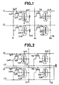
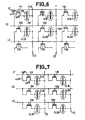
- - la figure 6, un schéma simplifié d'une matrice de commande d'un écran à cristal liquide selon l'invention ;
- - la figure 7, un schéma simplifié d'une variante d'une matrice de commande d'un écran à cristal liquide selon l'invention ;
- - la figure 8, une vue en perspective d'un écran à cristal liquide selon l'art connu, conforme au schéma de la figure 6.
- - la figure 9, un schéma simplifié d'un circuit d'alimentation d'un écran de visualisation selon l'invention ;
- - la figure 10, un schéma simplifié d'une variante d'un circuit d'alimentation selon l'invention ;
- - la figure 11, un exemple de réalisation d'un point de croisement d'un écran de visualisation selon l'invention.
- - Figure 1, a simplified diagram of a control matrix of a liquid crystal screen according to the prior art, in which the row and column control conductors cross on the same face of the liquid crystal cell ;
- - Figure 2, a simplified diagram of a control matrix of a liquid crystal screen according to the prior art, in which the row and column control conductors are separated by the liquid crystal cells;
- - Figure 3, a perspective view of an embodiment of a liquid crystal screen according to the prior art, according to the diagram of Figure 1;
- - Figures 4 and 5, simplified diagrams equipped with capacitor for storing crossing points according to the prior art;
- - Figure 6, a simplified diagram of a control matrix of a liquid crystal screen according to the invention;
- - Figure 7, a simplified diagram of a variant of a control matrix of a liquid crystal screen according to the invention;
- FIG. 8, a perspective view of a liquid crystal screen according to the prior art, in accordance with the diagram of FIG. 6.
- - Figure 9, a simplified diagram of a supply circuit of a display screen according to the invention;
- - Figure 10, a simplified diagram of a variant of a supply circuit according to the invention;
- - Figure 11, an embodiment of a crossing point of a display screen according to the invention.
En se reportant à la figure 1, on va tout d'abord décrire un schéma simplifié d'une matrice de commande à transistors d'un écran à cristal liquide.Referring to Figure 1, we will first describe a simplified diagram of a transistor control matrix of a liquid crystal screen.
Comme cela est connu dans la technique, un écran à cristal liquide comporte essentiellement deux plaques en verre enserrant un cristal liquide. Les faces internes de ces plaques, en contact avec le cristal liquide, portent les circuits de l'écran à cristal liquide.As is known in the art, a liquid crystal screen essentially comprises two glass plates enclosing a liquid crystal. The internal faces of these plates, in contact with the liquid crystal, carry the circuits of the liquid crystal screen.
La matrice de commande de l'écran est située sur l'une de ses faces. Elle comporte comme représenté en figure 1, des conducteurs de lignes L1 et L2 et des conducteurs de colonnes K1 et K2. Les conducteurs de lignes et de colonnes se croisent sans qu'il y ait connexion entre eux. A chaque croisement entre un conducteur de ligne et un conducteur de colonne est connecté un transistor ayant sa grille connectée à une ligne et sa source à une colonne. Ainsi, au croisement de la ligne L1 et de la colonne K1 est connecté un transistor T11 possédant une grille connectée par une connexion de grille cg 11 à la ligne L1 et une source connectée par une connexion de source cs11 à la colonne K1. Sur la même face de l'écran que les lignes L1, L2, colonnes K1, K2 et transistors T11 sont implantés des électrodes métalliques au croisement de chaque ligne et chaque colonne. Chacune de ces électrodes est connectée au drain d'un transistor précédemment décrit. C'est ainsi, qu'au croisement de la ligne L1 et de la colonne K1, une électrode E11 est connectée par une connexion de drain cd11 au drain du transistor T11.The screen control matrix is located on one of its faces. As shown in FIG. 1, it comprises row conductors L1 and L2 and column conductors K1 and K2. The row and column conductors cross without any connection between them. At each crossing between a row conductor and a column conductor is connected a transistor having its gate connected to a line and its source to a column. Thus, at the intersection of line L1 and column K1 is connected a transistor T11 having a gate connected by a
Sur l'autre face de l'écran, en vis-à-vis de chaque électrode, telle que E11 est implantée une électrode. Cette électrode est connectée à la masse. En pratique, toutes les électrodes de cette face, étant connectées à la masse, sont constituées d'une seule plaque de masse.On the other side of the screen, facing each electrode, such as E11 is an electrode. This electrode is connected to ground. In practice, all the electrodes of this face, being connected to ground, consist of a single ground plate.
Une telle configuration d'écran est représentée en perspective sur la figure 3. Sur cette figure on trouve sur une face 10 d'une première lame 1 les conducteurs de ligne L1 et L2, les conducteurs de colonnes K1, K2 et K3. Connectés sensiblement à chaque point de croisement, on trouve également des transistors et des électrodes tels que le transistor T11 et l'électrode E11 situés au croisement du conducteur de ligne L1 et du conducteur de colonne K1.Such a screen configuration is shown in perspective in FIG. 3. In this figure are found on a
Une deuxième lame 2, de préférence en verre, détermine avec une de ces faces 20 et la face 10 de la lame 1, un espace 3 dans lequel est placé un cristal liquide.A
La face 20 une plaque de masse également transparente. Une électrode de la face 10 telle que E11, la plaque de masse en vis-à-vis et le cristal liquide qui les séparent constituent une cellule à cristal liquide CL11 de l'écran.The
Le fonctionnement d'un tel écran est connu. Rappelons simplement que pour afficher une information sur une cellule de cristal liquide, il faut appliquer à une ligne (L1 par exemple) et une colonne (K1 par exemple) des potentiels appropriés rendant conducteur le transistor T11 qui applique alors un potentiel à l'électrode E11 de telle façon que les électrodes E11 et F11 de la cellule CL11 soient soumises à une différence de potentiel permettant un changement d'état du cristal liquide la cellule CL11.The operation of such a screen is known. Let us simply recall that to display information on a liquid crystal cell, it is necessary to apply to a row (L1 for example) and a column (K1 for example) suitable potentials making the transistor T11 conductive which then applies a potential to the electrode E11 in such a way that the electrodes E11 and F11 of the cell CL11 are subjected to a potential difference allowing a change of state of the liquid crystal in the cell CL11.
Pour que cet écran fonctionne convenablement, il faut qu'il n'existe aucun contact entre les conducteurs de ligne L1, L2 et les conducteurs de colonne K1, K2, K3. Comme on peut le voir sur la figure 3, il faut donc que ces conducteurs soient convenablement isolés pour éviter ces contacts soit directement au niveau des points de croisement, soit par l'intermédiaire du cristal liquide.For this screen to function properly, there must be no contact between the line conductors L1, L2 and the column conductors K1, K2, K3. As can be seen in Figure 3, it is therefore necessary that these conductors are suitably insulated to avoid these contacts either directly at the crossing points, or through the liquid crystal.
Pour éviter des croisements entre conducteurs de ligne et conducteurs de colonne il est connu, comme cela est décrit dans la demande de brevet français N° 2 553 218 publiée le 12 avril 1985, de dédoubler les conducteurs de ligne.To avoid crossovers between line conductors and column conductors, it is known, as described in French patent application No. 2,553,218 published on April 12, 1985, to split line conductors.
Une telle solution est représentée en figure 2. On retrouve sur cette figure le réseau de conducteurs de ligne L1 et L2, la matrice de transistors T11, T12, T21, T22 et la matrice d'électrodes E11, E12, E21, E22. En plus de ces éléments agencés sur une face 10 d'une lame 1 de l'écran à cristal liquide, est disposé un deuxième réseau de conducteurs de ligne L'1, L'2 parallèles aux conducteurs de ligne L1, L2. Les connexions de source connectent alors les sources des transistors à ces conducteurs de ligne L'1 et L'2. C'est ainsi que le transistor T11 a sa grille connectée au conducteur de ligne L1, sa source connectée au conducteur de ligne L'1, son drain don- necté à l'électrode E11.Such a solution is shown in FIG. 2. This figure shows the network of line conductors L1 and L2, the matrix of transistors T11, T12, T21, T22 and the matrix of electrodes E11, E12, E21, E22. In addition to these elements arranged on one
Sur la face 20 de la deuxième lame 2 de l'écran, les électrodes F11 à F22 sont connectées à des conducteurs de colonnes C1, C2.On the
Les conducteurs de ligne L'1 et L'2 sont connectés à un potentiel de référence telle que la masse. Le fonctionnement de cet écran et la commande d'une cellule à cristal liquide CL1 1 se fait par application de potentiels appropriés sur les conducteurs de ligne, tel que L1, et les conducteurs de colonne tel que C1.The line conductors L'1 and L'2 are connected to a reference potential such as ground. The operation of this screen and the control of a liquid
Il est à noter que dans les types d'écrans décrits précédemment, on prévoit à chaque point de croisement un condensateur de stockage permettant d'accroître l'effet mémoire de chaque cellule à cristal liquide. Sur les figures 4 et 5, on a représenté un point de croisement du type d'écran de la figure 1. Sur la figure 4, un condensateur de stockage CK11 a été connecté entre le drain du transistor T11 et le conducteur de ligne L1. Il est possible, comme représenté en figure 5, de connecter un condensateur de stockage CK11 entre le drain du transistor T11 et un conducteur de ligne voisin L2.It should be noted that in the types of screens described above, a storage capacitor is provided at each crossing point allowing the memory effect of each liquid crystal cell to be increased. In FIGS. 4 and 5, a crossing point of the type of screen in FIG. 1 has been shown. In FIG. 4, a storage capacitor CK11 has been connected between the drain of the transistor T11 and the line conductor L1. It is possible, as shown in FIG. 5, to connect a storage capacitor CK11 between the drain of the transistor T11 and a neighboring line conductor L2.
Comme on peut le constater dans la description qui précède, la fabrication d'un écran de type connu, nécessite l'implantation sur une même face de l'écran à cristal liquide, soit de réseaux de conducteurs qui se croisent mais isolés les uns des autres, soit de deux réseaux de conducteurs de ligne.As can be seen in the above description, the manufacture of a screen of known type requires the installation on the same face of the liquid crystal screen, that is to say networks of conductors which cross but isolated from each other. others, or two networks of line conductors.
L'invention concerne un écran de visualisation de structure plus simple donc plus facile à réaliser et moins susceptible de défauts de fabrication, donc plus fiable.The invention relates to a simpler structure display screen therefore easier to produce and less susceptible to manufacturing defects, therefore more reliable.
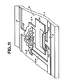
En se reportant aux figures 6 et 8, en va décrire un exemple de réalisation d'un écran selon l'invention.Referring to Figures 6 and 8, will describe an embodiment of a screen according to the invention.
Cet écran comporte deux lames de verre 1 et 2 disposées parallèlement. Entre ces deux lames de verre 1 et 2 est placé un matériau électrooptique 3 en contact avec les faces 10 et 20 de ces lames.This screen comprises two
Sur la face 10 de la lame 1 est disposé une matrice d'électrodes E11 à E23 arrangées en lignes et colonnes. Parallèlement aux lignes d'électrodes sont disposées des conducteurs de lignes L1 à L3.On the
A chaque électrode est associé un transistor T11 1 à T33. La grille de chacun des transistors d'une ligne est connectée à un conducteur de ligne associé. La source de ces transistors est connectée à un conducteur de ligne voisin. Le drain de chaque transistor est connecté à l'électrode associée au transistor.Each electrode is associated with a
C'est ainsi que la grille du transistor T11 est connectée par une connexion de grille cg11 à un conducteur de ligne L1, que la source de ce transistor est connectée par une connexion de source cs11 au conducteur de ligne suivante L2 et que le drain est connecté à une électrode E11 par une connexion de drain cd 11.Thus the gate of transistor T11 is connected by a gate connection cg11 to a line conductor L1, that the source of this transistor is connected by a source connection cs11 to the next line conductor L2 and that the drain is connected to an electrode E11 by a
La face 20 de la lame 2 porte des électrodes situées en regard des électrodes E11 à E23. Sur la figure 6, on a représenté une électrode, telle que F11, en face de chaque électrode E11 à E23. Un couple d'électrodes tel que E11 - F11 et le cristal liquide situé entre ces électrodes constitue une cellule à cristal liquide CL11. Les électrodes de la face 20 constituant une même colonne sont connectées à un conducteur de colonne C1, C2.The
Sur la figure 8, les électrodes de la face 20 sont réalisées sous forme d'électrodes allongées C1, C2 correspondant chacune à une colonne d'électrodes de la face 10. Chaque électrode C1, C2 tient donc lieu également de conducteur de colonne.In FIG. 8, the electrodes of the
La commande d'une cellule, CL11 par exemple, se fait par application d'un potentiel de commande de grille Vg sur une ligne, L1 selon l'exemple puis, d'un potentiel d'alimentation de source Vs sur la ligne de rang suivant, donc la ligne L2 selon le même exemple. Par ailleurs, un potentiel de drain est appliqué sur le conducteur de colonne (ou électrode de colonne) C1.The control of a cell, CL11 for example, is done by application of a gate control potential Vg on a line, L1 according to the example then, of a source supply potential Vs on the row line next, so line L2 according to the same example. Furthermore, a drain potential is applied to the column conductor (or column electrode) C1.
A titre d'exemple, un transistor tel que T11 devient conducteur pour un potentiel de grille d'environ Vg = 15 volts et pour une tension drain-source d'environ Vd-Vs = 5 volts.By way of example, a transistor such as T11 becomes conductive for a gate potential of approximately Vg = 15 volts and for a drain-source voltage of approximately Vd-Vs = 5 volts.
Le fonctionnement d'une cellule implique que la commande d'une ligne de cellules empêche la commande des lignes de cellules voisines en raison du fait que les différents transistors sont connectés entre deux conducteurs de lignes. Cela impose un fonctionnement séquentiel de l'écran de l'invention, c'est-à-dire une commande séquentielle des différentes lignes de l'écran.The operation of a cell implies that the control of a line of cells prevents the control of the lines of neighboring cells due to the fact that the different transistors are connected between two line conductors. This requires a sequential operation of the screen of the invention, that is to say a sequential control of the different lines of the screen.
Par ailleurs, bien que cela ne soit pas représenté sur les figures, il est possible de connecter, pour chaque transistor, un condensateur de stockage entre la connexion de drain cd 11 du transistor et le conducteur de ligne L1 auquel est connecté son conducteur de grille ou bien, au conducteur de ligne L2 auquel est connecté son conducteur de source.Furthermore, although this is not shown in the figures, it is possible to connect, for each transistor, a storage capacitor between the
En se reportant à la figure 9, on va donc maintenant décrire des circuits permettant de mettre en oeuvre l'écran de l'invention.Referring to Figure 9, we will now describe circuits for implementing the screen of the invention.
Sur cette figure, on a représenté un écran comportant une matrice de m x n cellules arrangées en m lignes et n colonnes. A ces cellules sont associés m x n transistors T11 à Tmn.In this figure, a screen is shown comprising a matrix of m x n cells arranged in m rows and n columns. These cells are associated with m × n transistors T11 to Tmn.
La commande de ces cellules se fait à l'aide de m+1 conducteurs de lignes L1 à Lm+1 et n conducteurs de colonnes C1 à Cn.These cells are controlled using m + 1 row conductors L1 to Lm + 1 and n column conductors C1 to Cn.
Trois générateurs Gg, Gs et Gd fournissent respectivement des potentiels de grille, de seuil et de drain appropriés pour la conduction des transistors.Three generators Gg, Gs and Gd respectively provide gate, threshold and drain potentials suitable for the conduction of the transistors.
Les générateurs Gg et Gs sont connectables aux conducteurs de lignes L1 à Lm par des circuits de connexion AL1 à ALm. Un circuit de connexion AL1 à ALm connecte le générateur Gg au conducteur de ligne correspondant lorsqu'il reçoit un signal de commande de niveau 1 sur son entrée d1. Lorsqu'il reçoit un signal de niveau O au lieu d'un signal de niveau 1, il connecte à la place le générateur Gs au conducteur de ligne.The generators Gg and Gs are connectable to the line conductors L1 to Lm by connection circuits AL1 to ALm. A connection circuit AL1 to ALm connects the generator Gg to the corresponding line conductor when it receives a
Un distributeur Dm fournit un signal de niveau 1 sur une seule sortie d1 à dm. Il fournit ce signal successivement sur toutes les sorties d1 à dm. Lorsqu'il fournit un signal de niveau 1 sur une sortie, il fournit un signal de niveau O sur toutes les autres sorties. Un seul circuit de connexion AL1 à ALm à la fois connecte donc le générateur Gg à un conducteur de ligne tandis que les autres circuits de connexion connectent le générateur Gs aux autres conducteurs de ligne.A Dm distributor provides a
Un générateur Gd permet d'alimenter simultanément sous différents niveaux de tension les conducteurs de colonnes déterminant ainsi la commande de transistors et des cellules associées sous différents niveaux de tension.A generator Gd enables the column conductors to be supplied simultaneously at different voltage levels, thus determining the control of transistors and associated cells under different voltage levels.
Le circuit de la figure 9 permet ainsi de réaliser une commande séquentielle ligne par ligne de l'écran. Par exemple, lorsque le distributeur Dm fournit un signal de niveau 1 sur sa sortie d1 et un signal de niveau 0 sur toutes ses autres sorties, seul le circuit de connexion A11 connecte le générateur Gg au conducteur de ligne L1, les autres circuits de connexion, et notamment AL2, connectent le générateur Gs aux autres conducteurs de ligne L2 à Lm. Le conducteur de ligne L1 est au potentiel Vg et les autres conducteurs de lignes sont tous au potentiel Vs.The circuit of FIG. 9 thus makes it possible to carry out a sequential control line by line of the screen. For example, when the distributor Dm provides a
Le distributeur Dn fournit à chaque conducteur de colonne, un potentiel de commande particulier fourni par le générateur Gd. Les cellules de la lignes L1 sont ainsi commandées chacune sous un niveau de tension particulier.The distributor Dn supplies each column conductor with a specific control potential supplied by the generator Gd. The cells of line L1 are thus each controlled under a particular voltage level.
Les transistors T1 et T12 situés aux points de croisement du conducteur de ligne L1 et des conducteurs de colonnes C1 et C2 commandés sont rendus conducteurs et les cellules associées CL11 et CL12 changent d'état.The transistors T1 and T12 located at the crossing points of the line conductor L1 and of the column conductors C1 and C2 controlled are made conductive and the associated cells CL11 and CL12 change state.
Le distributeur Dm fournit ensuite un signal de niveau 1 sur la sortie d2. Le circuit de connexion AL2 connecte le générateur Gg au conducteur de ligne L2, tandis que le générateur Gs est connecté aux autres conducteurs de ligne. Le distributeur Dn connecte le générateur Gd aux conducteurs de colonne C1 à Cn appropriés déterminant la commande de cellules connectées au conducteur de ligne L2.The distributor Dm then supplies a
La matrice de l'écran est ainsi explorée ligne par ligne:The screen matrix is thus explored line by line:
La distribution des commandes de connexion aux circuits de connexion AL1 à ALm peut être réalisée simplement, comme cela est représenté en figure 10, à l'aide d'un registre à décalage REG.The distribution of the connection commands to the connection circuits AL1 to ALm can be carried out simply, as shown in FIG. 10, using a shift register REG.
Ce registre REG comporte autant d'étages A1 à Am qu'il y a de conducteurs de ligne. Il est alimenté par un générateur Gg fournissant un potentiel de grille Vg et un générateur Gs fournissant un potentiel de seuil Vs.This register REG comprises as many stages A1 to Am as there are line conductors. It is supplied by a generator Gg providing a gate potential Vg and a generator Gs providing a threshold potential Vs.
Un conducteur de ligne L1 à Lm est connecté à chaque étage A1 à Am. Lorsqu'un étage est à l'état 0, il fournit un potentiel de source Vs sur le conducteur de ligne qui lui est connecté. Lorsqu'un étage est à l'état 1, il fournit un potentiel de grille sur le conducteur de ligne.A line conductor L1 to Lm is connected to each stage A1 to Am. When a stage is at
Un circuit de commande DEC fournit un signal de niveau logique 1 à une entrée du premier étage et commande son décalage dans les étages successifs du registre, commandant l'alimentation du potentiel Vg sur les conducteurs de ligne successifs L1 à Lm, un seul conducteur de ligne à la fois étant au potentiel Vg tandis que les autres sont au potentiel Vs. L'alimentation par le générateur Gd et le distributeur Dn, des conducteurs de colonne C1 à Cn est réalisée comme décrite en se reportant à la figure 9. On réalise ainsi une commande séquentielle ligne par ligne de l'écran.A control circuit DEC supplies a signal of
Selon une variante de l'invention, les sources des transistors d'une ligne de la matrice de l'écran au lieu d'être connectées au conducteur de ligne de rang suivant, sont connectées au même conducteur de ligne que les grilles des mêmes transistors. On obtient alors une matrice telle que représentée en figure 7.According to a variant of the invention, the sources of the transistors of a line of the screen matrix, instead of being connected to the line conductor of the next rank, are connected to the same line conductor as the gates of the same transistors . We then obtain a matrix as shown in FIG. 7.
Dans ce mode de réalisation, le potentiel de commande appliqué à un conducteur de ligne pourra être d'environ Vg = 15 volts, tandis que le potentiel de commande appliqué à un conducteur de colonne sera alors nettement inférieur tel que Vd = 5 volts environ.In this embodiment, the control potential applied to a line conductor may be around Vg = 15 volts, while the control potential applied to a column conductor will then be much lower such that Vd = 5 volts.
Un point de croisement selon l'invention et son transistor tel que T11 peuvent être réalisés comme cela est représenté à titre d'exemple en figure 11.A crossing point according to the invention and its transistor such as T11 can be produced as shown by way of example in FIG. 11.
Sur cette figure 11 on retrouve les conducteurs de lignes L1 et L2 ainsi que l'électrode E11 disposés sur la face 10 de la plaque 1.In this figure 11 we find the line conductors L1 and L2 as well as the electrode E11 arranged on the
Un conducteur métallique ou connexion de grille cg11 est connecté au conducteur de ligne L1. Sur cette connexion de grille et transversalement sont déposées successivement une couche t1 de matériau isolant, une couche t2 de semiconducteur tel que du silicium amorphe non dopé.A metallic conductor or grid connection cg11 is connected to the line conductor L1. On this gate connection and transversely are deposited successively a layer t1 of insulating material, a layer t2 of semiconductor such as undoped amorphous silicon.
Par ailleurs, un autre conducteur métallique CS11 1 est connecté au conducteur de ligne L2.Furthermore, another
Un conducteur métallique ou connexion de source cs11 permet de connecter le conducteur métallique CS11 à la couche t2 de semiconducteur.A metallic conductor or source connection cs11 makes it possible to connect the metallic conductor CS11 to the semiconductor layer t2.
De même, un autre conducteur métallique ou connexion de drain cd11 permet de connecter l'électrode E11 à la couche t2 de semiconducteur réalisant ainsi le canal du transistor.Similarly, another metallic conductor or drain connection cd11 makes it possible to connect the electrode E11 to the layer t2 of the semiconductor thus producing the transistor channel.
Le point de croisement de l'invention est ainsi réalisé.The cross point of the invention is thus achieved.
Par ailleurs, sur la figure 11 on a représenté la réalisation d'une capacité de stockage CK11 intégrée au dispositif de l'invention. Pour cela, avant dépôt de l'électrode E11, un élément conducteur ck1 connecté au conducteur de ligne L2 est prévu sur la face 10 de la plaque 1. L'élément conducteur ck1 est revêtu d'une couche d'un matériau isolant ck2. Sur cet ensemble élément conducteur ck1 et isolant ck2 est déposé l'électrode E1 pour constituer une capacité de stockage.Furthermore, in FIG. 11 is shown the production of a storage capacity CK11 integrated into the device of the invention. For this, before depositing the electrode E11, a conductive element ck1 connected to the line conductor L2 is provided on the
Il est à noter que selon les exemples de réalisation décrits précédemment, on a prévu de connecter les sources des transistors à des conducteurs de ligne tandis que les drains sont connectés à des conducteurs de colonnes. Ces connexions pourraient être inversées, étant entendu que les sens d'alimentation seraient alors eux aussi inversés.It should be noted that according to the examples of realization tion previously described, provision has been made to connect the sources of the transistors to line conductors while the drains are connected to column conductors. These connections could be reversed, it being understood that the supply directions would then also be reversed.
Claims (10)
Applications Claiming Priority (2)
| Application Number | Priority Date | Filing Date | Title |
|---|---|---|---|
| FR8516935A FR2590394B1 (en) | 1985-11-15 | 1985-11-15 | ELECTRO-OPTICAL VISUALIZATION SCREEN WITH CONTROL TRANSISTORS |
| FR8516935 | 1985-11-15 |
Publications (2)
| Publication Number | Publication Date |
|---|---|
| EP0228317A1 EP0228317A1 (en) | 1987-07-08 |
| EP0228317B1 true EP0228317B1 (en) | 1990-04-25 |
Family
ID=9324866
Family Applications (1)
| Application Number | Title | Priority Date | Filing Date |
|---|---|---|---|
| EP86402508A Expired - Lifetime EP0228317B1 (en) | 1985-11-15 | 1986-11-12 | Electro-optical display screen with control transistors |
Country Status (5)
| Country | Link |
|---|---|
| US (1) | US4818991A (en) |
| EP (1) | EP0228317B1 (en) |
| JP (1) | JP2617180B2 (en) |
| DE (1) | DE3670710D1 (en) |
| FR (1) | FR2590394B1 (en) |
Families Citing this family (18)
| Publication number | Priority date | Publication date | Assignee | Title |
|---|---|---|---|---|
| FR2571526B1 (en) * | 1984-08-22 | 1991-02-08 | Canon Kk | DISPLAY PANEL AND ITS CONTROL METHOD |
| KR900004989B1 (en) * | 1986-09-11 | 1990-07-16 | Fujitsu Ltd | Active matrix type display and driving method |
| EP0283290B1 (en) * | 1987-03-18 | 1994-09-21 | Matsushita Electric Industrial Co., Ltd. | Video projector |
| US5075674A (en) * | 1987-11-19 | 1991-12-24 | Sharp Kabushiki Kaisha | Active matrix substrate for liquid crystal display |
| GB2212659A (en) * | 1987-11-20 | 1989-07-26 | Philips Electronic Associated | Multi-level circuit cross-overs |
| FR2625827B1 (en) * | 1988-01-11 | 1993-07-16 | Commissariat Energie Atomique | COLOR DISPLAY WITH ACTIVE MATRIX WITHOUT CROSSING OF CONDUCTORS ADDRESSING LINES AND CONDUCTORS CONTROL COLUMNS |
| JP2565391B2 (en) * | 1988-12-23 | 1996-12-18 | アイシン高丘株式会社 | Molding method for vanishing model with core |
| JP2816979B2 (en) * | 1989-02-13 | 1998-10-27 | 日本フィリップス株式会社 | Display device with input function |
| EP0434626A3 (en) * | 1989-12-18 | 1991-10-30 | Ois Optical Imaging Systems, Inc. | Macroscopically sized liquid crystal display |
| JPH04226079A (en) * | 1990-04-17 | 1992-08-14 | Canon Inc | Semiconductor device and its manufacture and electronic circuit device using it |
| FR2693305B1 (en) * | 1992-07-02 | 1994-09-30 | Sagem | Liquid crystal display device, active matrix. |
| US5426447A (en) | 1992-11-04 | 1995-06-20 | Yuen Foong Yu H.K. Co., Ltd. | Data driving circuit for LCD display |
| JP2626451B2 (en) * | 1993-03-23 | 1997-07-02 | 日本電気株式会社 | Driving method of liquid crystal display device |
| US5694155A (en) * | 1995-04-25 | 1997-12-02 | Stapleton; Robert E. | Flat panel display with edge contacting image area and method of manufacture thereof |
| KR100230793B1 (en) * | 1995-07-28 | 1999-11-15 | 김영환 | LCD Drives |
| US5757351A (en) * | 1995-10-10 | 1998-05-26 | Off World Limited, Corp. | Electrode storage display addressing system and method |
| JP3147104B2 (en) * | 1998-11-06 | 2001-03-19 | 日本電気株式会社 | Active matrix type liquid crystal display device and driving method thereof |
| JP2005062396A (en) * | 2003-08-11 | 2005-03-10 | Sony Corp | Display device and driving method thereof |
Family Cites Families (8)
| Publication number | Priority date | Publication date | Assignee | Title |
|---|---|---|---|---|
| US3824003A (en) * | 1973-05-07 | 1974-07-16 | Hughes Aircraft Co | Liquid crystal display panel |
| DE2953769C2 (en) * | 1978-02-08 | 1985-02-14 | Sharp K.K., Osaka | Liquid crystal display matrix with thin film transistor arrangement |
| GB2042238B (en) * | 1979-02-14 | 1982-12-08 | Matsushita Electric Industrial Co Ltd | Drive circuit for a liquid crystal display panel |
| US4470060A (en) * | 1981-01-09 | 1984-09-04 | Semiconductor Energy Laboratory Co., Ltd. | Liquid crystal display with vertical non-single crystal semiconductor field effect transistors |
| JPS57204592A (en) * | 1981-06-11 | 1982-12-15 | Sony Corp | Two-dimensional address device |
| US4525710A (en) * | 1982-02-16 | 1985-06-25 | Seiko Instruments & Electronics Ltd. | Picture display device |
| FR2553218B1 (en) * | 1983-10-07 | 1987-09-25 | Commissariat Energie Atomique | ACTIVE MATRIX DISPLAY SCREEN WITHOUT CROSSING LINES AND ADDRESSING COLUMNS |
| US4537471A (en) * | 1983-12-23 | 1985-08-27 | Hughes Aircraft Company | Liquid crystal pixel driver circuit and matrix display |
-
1985
- 1985-11-15 FR FR8516935A patent/FR2590394B1/en not_active Expired
-
1986
- 1986-11-06 US US07/927,851 patent/US4818991A/en not_active Expired - Fee Related
- 1986-11-12 DE DE8686402508T patent/DE3670710D1/en not_active Expired - Fee Related
- 1986-11-12 EP EP86402508A patent/EP0228317B1/en not_active Expired - Lifetime
- 1986-11-14 JP JP61271633A patent/JP2617180B2/en not_active Expired - Lifetime
Also Published As
| Publication number | Publication date |
|---|---|
| FR2590394B1 (en) | 1987-12-18 |
| EP0228317A1 (en) | 1987-07-08 |
| JPS62119574A (en) | 1987-05-30 |
| JP2617180B2 (en) | 1997-06-04 |
| FR2590394A1 (en) | 1987-05-22 |
| US4818991A (en) | 1989-04-04 |
| DE3670710D1 (en) | 1990-05-31 |
Similar Documents
| Publication | Publication Date | Title |
|---|---|---|
| EP0228317B1 (en) | Electro-optical display screen with control transistors | |
| EP0267824B1 (en) | Transistor-driven electro-optical visualization screen, and method of manufacturing it | |
| EP0216673B1 (en) | Method for producing a control transistor for a flat viewing screen, and control element manufactured thereby | |
| EP0145520B1 (en) | Display screen with active matrix without intersection of the row and column address lines | |
| EP1332519B1 (en) | Tft matrix for optical sensor comprising a photosensitive semiconductor layer, and optical sensor comprising such an active matrix | |
| FR2604014A1 (en) | INFORMATION CONVERSION DEVICE HAVING AUXILIARY ADDRESS LINES TO IMPROVE MANUFACTURING OUTPUT | |
| FR2488013A1 (en) | ACTIVE MATRIX MATRIX DEVICE | |
| FR2530057A1 (en) | Dot matrix liquid crystal display | |
| FR2702286A1 (en) | Liquid crystal display and method of making the same | |
| EP0200599B1 (en) | Method of producing non-linear control elements for an electro-optical, flat image screen, and flat screen produced by this method | |
| JP2001511317A (en) | Thin film transistor and electronic device comprising the thin film transistor | |
| EP0506528B1 (en) | Matrix driving structure for display screen | |
| EP0246945A1 (en) | Electrooptic screen display and method for its manufacture | |
| EP0493178A1 (en) | Matrix colour screen with triangular colour filter | |
| EP0041890B1 (en) | Element with non-linear conductivity, and switching circuit, especially for image display with such an element | |
| EP0392918B1 (en) | Electroluminescent display screen with memory and with a particular configuration of electrodes | |
| EP0564337A1 (en) | Display screen with optical mask and procedure for realization of this screen | |
| US4662719A (en) | Liquid crystal display and method for production | |
| EP1567911A1 (en) | Active matrix structure for display screen and screen comprising one such matrix | |
| EP0266252B1 (en) | Transistor-driven electro-optic display and its manufacturing method | |
| FR2602362A1 (en) | MATRIX DISPLAY DEVICE COMPRISING TWO PACKETS OF LINEAR ELECTRODES AND TWO ELECTRODES COLLECTED BY IMAGE ELEMENT AND ITS CONTROL METHOD | |
| FR2605443A1 (en) | ELECTROOPTICAL DISPLAY SCREEN WITH CONTROL TRANSISTOR AND METHOD OF MAKING SAME | |
| WO2006092473A1 (en) | Oled pixel layout | |
| EP0194947A2 (en) | Point matrix display device | |
| KR20010006946A (en) | Active matrix array substrate and its manufacturing method |
Legal Events
| Date | Code | Title | Description |
|---|---|---|---|
| PUAI | Public reference made under article 153(3) epc to a published international application that has entered the european phase |
Free format text: ORIGINAL CODE: 0009012 |
|
| AK | Designated contracting states |
Kind code of ref document: A1 Designated state(s): DE GB NL |
|
| 17P | Request for examination filed |
Effective date: 19870821 |
|
| RAP3 | Party data changed (applicant data changed or rights of an application transferred) |
Owner name: THOMSON-CSF |
|
| 17Q | First examination report despatched |
Effective date: 19890714 |
|
| GRAA | (expected) grant |
Free format text: ORIGINAL CODE: 0009210 |
|
| AK | Designated contracting states |
Kind code of ref document: B1 Designated state(s): DE GB NL |
|
| REF | Corresponds to: |
Ref document number: 3670710 Country of ref document: DE Date of ref document: 19900531 |
|
| GBT | Gb: translation of ep patent filed (gb section 77(6)(a)/1977) | ||
| PLBE | No opposition filed within time limit |
Free format text: ORIGINAL CODE: 0009261 |
|
| STAA | Information on the status of an ep patent application or granted ep patent |
Free format text: STATUS: NO OPPOSITION FILED WITHIN TIME LIMIT |
|
| 26N | No opposition filed | ||
| PGFP | Annual fee paid to national office [announced via postgrant information from national office to epo] |
Ref country code: NL Payment date: 19991013 Year of fee payment: 14 |
|
| PGFP | Annual fee paid to national office [announced via postgrant information from national office to epo] |
Ref country code: GB Payment date: 19991014 Year of fee payment: 14 |
|
| PGFP | Annual fee paid to national office [announced via postgrant information from national office to epo] |
Ref country code: DE Payment date: 19991015 Year of fee payment: 14 |
|
| PG25 | Lapsed in a contracting state [announced via postgrant information from national office to epo] |
Ref country code: GB Free format text: LAPSE BECAUSE OF NON-PAYMENT OF DUE FEES Effective date: 20001112 |
|
| PG25 | Lapsed in a contracting state [announced via postgrant information from national office to epo] |
Ref country code: NL Free format text: LAPSE BECAUSE OF NON-PAYMENT OF DUE FEES Effective date: 20010601 |
|
| GBPC | Gb: european patent ceased through non-payment of renewal fee |
Effective date: 20001112 |
|
| NLV4 | Nl: lapsed or anulled due to non-payment of the annual fee |
Effective date: 20010601 |
|
| PG25 | Lapsed in a contracting state [announced via postgrant information from national office to epo] |
Ref country code: DE Free format text: LAPSE BECAUSE OF NON-PAYMENT OF DUE FEES Effective date: 20010801 |