EP0225822A1 - Multiple-track capacitor - Google Patents
Multiple-track capacitor Download PDFInfo
- Publication number
- EP0225822A1 EP0225822A1 EP86402460A EP86402460A EP0225822A1 EP 0225822 A1 EP0225822 A1 EP 0225822A1 EP 86402460 A EP86402460 A EP 86402460A EP 86402460 A EP86402460 A EP 86402460A EP 0225822 A1 EP0225822 A1 EP 0225822A1
- Authority
- EP
- European Patent Office
- Prior art keywords
- zones
- capacitor
- multitrack
- films
- capacitors
- Prior art date
- Legal status (The legal status is an assumption and is not a legal conclusion. Google has not performed a legal analysis and makes no representation as to the accuracy of the status listed.)
- Granted
Links
Images


Classifications
-
- H—ELECTRICITY
- H01—ELECTRIC ELEMENTS
- H01G—CAPACITORS; CAPACITORS, RECTIFIERS, DETECTORS, SWITCHING DEVICES OR LIGHT-SENSITIVE DEVICES, OF THE ELECTROLYTIC TYPE
- H01G4/00—Fixed capacitors; Processes of their manufacture
- H01G4/38—Multiple capacitors, i.e. structural combinations of fixed capacitors
- H01G4/385—Single unit multiple capacitors, e.g. dual capacitor in one coil
-
- H—ELECTRICITY
- H01—ELECTRIC ELEMENTS
- H01G—CAPACITORS; CAPACITORS, RECTIFIERS, DETECTORS, SWITCHING DEVICES OR LIGHT-SENSITIVE DEVICES, OF THE ELECTROLYTIC TYPE
- H01G4/00—Fixed capacitors; Processes of their manufacture
- H01G4/002—Details
- H01G4/005—Electrodes
- H01G4/015—Special provisions for self-healing
Definitions
- the present invention relates to capacitors of the multitrack type and in particular to wound capacitors.
- Multitrack wound capacitors are already known, for example from the document GB-A-759 026 which describes capacitors of the type comprising at least three electrodes separated by sheets of a dielectric. These electrodes and dielectric sheets are arranged and wound so as to provide several individual capacitors which can be associated in series to form an equivalent capacitor supporting higher operating voltages than a conventional capacitor of the same size.
- the invention provides a multitrack capacitor obtained by winding at least two metallized dielectric films and the metallization of at least one of the films is crenellated so as to form electrodes of elementary capacitors.
- the aliasing will be used for the formation of fusible zones used to limit the current during a possible breakdown in order to reduce the energy brought into play in the breakdown and thereby restrict the volatilized metallization portion.
- the fuse zone will be preserved after having played its role of current limiter. The loss of capacity when using the capacitor will then be minimal.
- the subject of the invention is therefore a multitrack capacitor of the type where the capacitance of the capacitor is obtained by the internal series connection of at least two individual capacitors, the capacitor being produced by winding at least two metallized dielectric films, the metallizations comprising areas intended to ensure the capacitive effect and areas of connections intended to ensure the internal series connection or the electrical connections with the external connections of the capacitor, characterized in that the metallization of at least one of the films is crenellated so as to form electrodes of elementary capacitors, the aliasing also allowing the formation of at least one fusible zone per series of elementary capacitors.
- the aliasing will advantageously be obtained from demetallized strips transverse and longitudinal to said films.
- the space separating two demetallized bands can be used to create the fusible zones, for example the space separating two successive longitudinal bands.
- metallizations can be made up of different resistivity zones.
- the zones intended to ensure the capacitive effect will be so-called zones with high resistivity with respect to the bonding zones which will be qualified as zones with low resistivity. These differences in resistivity between the different metallized zones may be due to differences in the thickness of these zones.
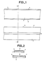
- Figures 1 and 2 are views of metallized dielectric films used to obtain by winding a multitrack capacitor according to the prior art. In the case shown it is a two-track type capacitor.
- Figure 1 is a top view of the films which have been shown side by side to facilitate understanding. In FIG. 2, these films are seen in section and are placed one above the other.
- the dielectric used can be a fibrous material such as paper or a synthetic material (polypropylene, polyester, etc.).
- the metallizations can be deposits of zinc, aluminum, another metal or an alloy.
- the film 1 supports an unfirome metallization 2 with the exception of the margins 3 and 4.
- the metallization of the film 5 consists of two parallel strips 6 and 7 separated by a non-metallized or demetallized zone 8.
- the film 1 is narrower than the film 5 so that, after winding, the "shooping" (realization of the external connections of the capacitor by metallization of its lateral faces according to the terminology used in man of the art) can be effectively achieved. Margins 3 and 4 are necessary to avoid possible short circuits during "shooping".
- Figure 2 shows the relative positioning of the two films before winding. After winding, they will be tightened one against the other. We will therefore obtain two individual capacitors: one between electrode 6 and electrode 2, the other between electrode 2 and electrode 7, the value of which will depend on the importance facing surfaces. These individual capacitors are arranged in series thanks to the electrical connection provided by the central area of the electrode 2.
- FIG. 3 and 4 show the metallized films of a two-track capacitor according to the invention.
- FIG. 4 in particular clearly shows, by comparison with FIG. 2, that these are indeed films intended for the production of a two-track capacitor.
- the dielectric film 10 supports a metallization 11 leaving margins 12 and 13.
- the dielectric film 14 supports metallizations 15 and 16 separated by a non-metallized or demetallized zone 17.
- the materials used for the films and the metallizations can be those of those already cited.
- the techniques for depositing metallizations on dielectric films are well known to those skilled in the art.
- the metallization 11 of the film 10 is crenellated to obtain electrodes of elementary capacitors and to add a fusible zone to them.
- the aliasing is for example made in the form of a succession of crosses.
- the transverse branch 18 of the cross joins the two margins 12 and 13 to create the elementary electrodes 19.
- the longitudinal branch 20 of the cross delimits a restricted width 21 of metallization to create a fusible zone.
- Other configurations of aliasing are of course possible.
- the fuse zone may not be located in the center of the electrode 19. It may be located towards one of the edges of this electrode, for example between the end of the demetallized strip 20 and the demetallized strip 18.
- the aliasing may be produced in different ways: by chemical means, by sparking or by masking during the metallization of the film or better by ablation using a laser beam.
- each energy pulse volatilizes a metallization circle whose diameter can be adjusted between 0.1 and 2 mm.
- Optical scanning allows you to create a succession of intersecting circles to obtain a continuous demetallized line.
- the metallization can be on the ribbon or under the dielectric ribbon with respect to the laser beam. Whatever the respective positions of the metallization and of the laser beam, it is preferable to choose the wavelength of the laser beam in a range which corresponds to the zone of transparency of the ribbon in order to avoid its heating.
- a compromise between the power of the laser, the frequency of the energy pulses and the scanning speed is to be sought in order to carry out the demetallization without burning the dielectric tape which would cause untimely breakdowns when the capacitors are used.
- the metallized strips 15 and 16 can also be cut into electrodes 15 ′ and 16 ′ of elementary capacitors, in correspondence with the electrodes 19.
- the demetallized strips 22 can be perpendicular to the edges of the film 14 or inclined according to the demetallized bands 18.
- each individual capacitor being formed of a plurality of elementary capacitors having a fusible zone and associated in parallel.
- Figures 5 and 6 also show metallized films, but for a four-track capacitor according to the invention.
- the dielectric film 30, of smaller width than the film 31 supports two metallized strips 32 and 33 separated by a non-metallized or demetallized strip 34. Margins 35 and 36 are also provided.
- the film 31 supports three metallized strips 37, 38 and 39 separated by the non-metallized or demetallized strips 40 and 41.
- FIG. 6 we can see the existence of four capacitors in series: the first between bands 37 and 32, the second between bands 32 and 38, the third between bands 38 and 33 and the fourth between bands 33 and 39.
- the metallizations 37, 38 and 39 of film 31 are crenellated by transverse bands 42 perpendicular to the edges of the film 31 in the case of FIG.
- This aliasing principle is applicable to all multitrack capacitors with an even number of tracks.
- the metallized films may be identical, but the patterns are reversed on winding.
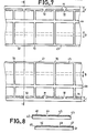
- Figures 7 and 8 show metallized films for a three-track capacitor according to the invention.
- the dielectric films 60 and 61 are of equal widths and will be wound offset as shown in FIG. 8.
- the film 60 supports two metallized strips 62 and 63 separated by a demetallized or non-metallized strip 64. It also has a non-metallized margin 65
- the film 61 supports the metallized bands 66 and 67 separated by a band 68 devoid of metallistion. It also has a non-metallized margin 69. Aliasing has been carried out on the metallizations of one of the films or identically on both as shown in FIG. 7. It consists of transverse demetallized strips 70 (perpendicular to the edges of the films or inclined) and longitudinal 71.
- fuse zones 72 make it possible to constitute fuse zones 72.
- FIG. 8 we note the existence of three capacitors in series: the first between the strips 62 and 66, the second between the strips 66 and 63 and the third between the strips 63 and 67. If the metallized films are identical, as is the case for FIG. 7, there are two fusible zones per series of three elementary capacitors. It is possible to have only one, for example by not making longitudinal cuts on one of the films.
- Multitrack wound capacitors have a serious drawback constituted by the very provision of the electrodes which induce weak points leading, by Corona effect, to a risk of deterioration of these capacitors.
- the metallization 2 is of high resistivity in order to ensure satisfactory self-healing, the metallizations 6 and 7 are of low resistivity to ensure a good electrical connection with the "shoopages".
- the strip 8 without metallization creates, when the capacitor is in operation, an edge effect contributing to the wear, by Corona effect, of the central area of metallization 2 because of its high resistivity. There is then a risk of deterioration of the capacitor by thermal runaway of the central area.
- the invention provides that the same metallization can have different resistivity zones: a so-called high resistivity zone and a so-called low resistivity zone. In practice, it will suffice to have a ratio of approximately four between the values of these resistivities.
- the central zone of the metallization 11 it is advantageous for the central zone of the metallization 11 to be of lower resistivity than the rest of this metallization. This central zone a is delimited, FIG. 3, by broken lines. To ensure effective "shooping", the outer edges of the metallizations 15 and 16 will also have a low resistivity. Figure 3, we delimited these edges under the reference b. Outside zones b, metallizations 15 and 16 will therefore be said to have high resistivity.
- the high resistivity metallization parts will ensure satisfactory self-healing.
- the metallization parts to low resistivity will ensure either a good electrical connection by "shooping", or will avoid wear by Corona effect.
- the metallization parts referenced c, d and e in FIG. 5 and referenced f and g in FIG. 7 will be of low resistivity.
- FIG. 9 repeats the case of the two-track capacitor of FIG. 4. A distinction is made in FIG. 9 of parts of metallization which are thicker than others which correspond to the absence of metallization on the film opposite.
- FIG. 10 shows the case of the four-track capacitor of FIG. 6.
- FIG. 11 shows the case of the three-track capacitor of FIG. 8.
- the fuse zones can be located in zones with low resistivity and risk not playing their fuse role properly. You can increase the resistance of the fuse by further reducing its width, but you cannot go beyond a certain limit. It is not possible at the same time to have a rapid layout of the demetallization laser beam and high geometric precision of this layout. Various tips can then be used.
- FIG. 12 is a variant of one of the films of FIG. 7.
- the two types of cuts 71 can be made from two lasers whose relative positions are well determined.
- FIG. 13 Another possible solution is shown in FIG. 13 where two demetallized strips 80 are terminated by two transverse cuts 81 which are perpendicular or inclined to them and the interval of which can be more easily determined than the distance separating the end of a demetallized strip at the beginning of 'another band.
- the aliasing of multitrack capacitors improves self-healing and practically doubles the voltage gradients on the film.
Landscapes
- Engineering & Computer Science (AREA)
- Power Engineering (AREA)
- Manufacturing & Machinery (AREA)
- Microelectronics & Electronic Packaging (AREA)
- Fixed Capacitors And Capacitor Manufacturing Machines (AREA)
Abstract
Description
La présente invention se rapporte aux condensateurs du type multipiste et notamment aux condensateurs bobinés.The present invention relates to capacitors of the multitrack type and in particular to wound capacitors.
Des condensateurs bobinés multipistes sont déjà connus, par exemple par le document GB-A-759 026 qui décrit des condensateurs du type comprenant au moins trois électrodes séparées par des feuilles d'un diélectrique. Ces électrodes et ces feuilles de diélectrique sont disposées et enroulées de manière à fournir plusieurs condensateurs individuels qui peuvent être associés en série pour former un condensateur équivalent supportant des tensions de service plus élevées qu'un condensateur classique de même encombrement.Multitrack wound capacitors are already known, for example from the document GB-A-759 026 which describes capacitors of the type comprising at least three electrodes separated by sheets of a dielectric. These electrodes and dielectric sheets are arranged and wound so as to provide several individual capacitors which can be associated in series to form an equivalent capacitor supporting higher operating voltages than a conventional capacitor of the same size.
Il est connu que, lors des contrôles en fin de fabrication ou de l'utilisation de tels condensateurs, les défauts de diélectrique donnent lieu à des décharges locales en forme d'arcs, oxydant ou volatilisant localement les métallisations. Ces décharges sont utiles car elles restaurent ainsi l'isolement normal. Ce processus est appelé auto-cicatrisation.It is known that, during controls at the end of manufacture or the use of such capacitors, the dielectric defects give rise to local discharges in the form of arcs, oxidizing or volatilizing locally the metallizations. These discharges are useful because they restore normal isolation. This process is called self-healing.
Cependant, pour des condensateurs d'une certaine capacité, et des tensions supérieures à quelques centaines de volts, l'énergie disponible pour une de ces décharges locales est telle que le condensateur peut être au moins localement détruit. Ce risque est d'autant plus grand que l'énergie stockée dans un condensateur est proportionnelle au carré de la tension, ce qui aggrave le danger de destruction dans le cas des condensateurs à haute tension.However, for capacitors of a certain capacity, and voltages greater than a few hundred volts, the energy available for one of these local discharges is such that the capacitor can be at least locally destroyed. This risk is all the greater as the energy stored in a capacitor is proportional to the square of the voltage, which increases the danger of destruction in the case of high voltage capacitors.
Pour pallier ces inconvénients, l'invention propose un condensateur multipiste obtenu par bobinage d'au moins deux films diélectriques métallisés et dont la métallisation d'au moins l'un des films est crénelée de façon à former des électrodes de condensateurs élémentaires. Le crénelage sera utilisé pour la formation de zones fusibles servant à limiter le courant lors d'un claquage éventuel afin de réduire l'énergie mise en jeu dans le claquage et de restreindre ainsi la partie de métallisation volatilisée. Dans la plupart des cas, la zone fusible sera préservée après avoir joué son rôle de limitateur de courant. La perte de capacité lors de l'utilisation du condensateur sera alors minimum.To overcome these drawbacks, the invention provides a multitrack capacitor obtained by winding at least two metallized dielectric films and the metallization of at least one of the films is crenellated so as to form electrodes of elementary capacitors. The aliasing will be used for the formation of fusible zones used to limit the current during a possible breakdown in order to reduce the energy brought into play in the breakdown and thereby restrict the volatilized metallization portion. In most cases, the fuse zone will be preserved after having played its role of current limiter. The loss of capacity when using the capacitor will then be minimal.
L'invention a donc pour objet un condensateur multipiste du type où la capacité du condensateur est obtenue par la mise en série interne d'au moins deux condensateurs individuels, le condensateur étant réalisé par bobinage d'au moins deux films diélectriques métallisés, les métallisations comprenant des zones destinées à assurer l'effet capacitif et des zones de liaisons destinées à assurer la mise en série interne ou les liaisons électriques avec les connexions externes du condensateur, caractérisé en ce que la métallisation d'au moins l'un des films est crénelée de façon à former des électrodes de condensateurs élémentaires, le crénelage permettant également la formation d'au moins une zone fusible par série de condensateurs élémentaires.The subject of the invention is therefore a multitrack capacitor of the type where the capacitance of the capacitor is obtained by the internal series connection of at least two individual capacitors, the capacitor being produced by winding at least two metallized dielectric films, the metallizations comprising areas intended to ensure the capacitive effect and areas of connections intended to ensure the internal series connection or the electrical connections with the external connections of the capacitor, characterized in that the metallization of at least one of the films is crenellated so as to form electrodes of elementary capacitors, the aliasing also allowing the formation of at least one fusible zone per series of elementary capacitors.
Le crénelage sera avantageusement obtenu à partir de bandes démétallisées transversales et longitudinales auxdits films.The aliasing will advantageously be obtained from demetallized strips transverse and longitudinal to said films.
L'espace séparant deux bandes démétallisées peut être mis à profit pour créer les zones fusibles, par example l'espace séparant deux bandes longitudinales successives.The space separating two demetallized bands can be used to create the fusible zones, for example the space separating two successive longitudinal bands.
Pour éviter les détériorations dues à l'effet Corona, les métallisations peuvent être constituées de zones de résistivités différentes. Les zones destinées à assurer l'effet capacitif seront des zones dites à résistivité élevée par rapport aux zones de liaison qui seront qualifiées de zones à faible résistivite. Ces différences de résistivité entre les différentes zones métallisées peuvent être dues à des différences d'épaisseur de ces zones.To avoid deterioration due to the Corona effect, metallizations can be made up of different resistivity zones. The zones intended to ensure the capacitive effect will be so-called zones with high resistivity with respect to the bonding zones which will be qualified as zones with low resistivity. These differences in resistivity between the different metallized zones may be due to differences in the thickness of these zones.
L'invention sera mieux comprise et d'autres avantages apparaîtront au moyen de la description qui va suivre et des figures annexées parmi lesquelles:
- - les figures 1 et 2 représentent des vues de dessus et en coupe de films diélectriques métallisés pour un condensateur multipiste selon l'art connu,
- - les figures 3 et 4 représentent des vues de dessus et en coupe de films diélectriques métallisés pour un condensateur multipiste selon l'invention,
- - les figures 5 et 6 représentent les mêmes vues pour une première variante de réalisation,
- - les figures 7 et 8 représentent les mêmes vues pour une seconde variante de réalisation,
- - les figures 9 à 11 représentent des vues en coupe de films diélectriques métallisés avec des métallisations renforcées,
- - la figure 12 représente une vue de dessus d'un film diélectrique métallisé pour un condensateur selon l'invention et possédant une zone fusible améliorée,
- - la figure 13 représente une variante de la zone fusible.
- FIGS. 1 and 2 show views from above and in section of metallized dielectric films for a multitrack capacitor according to known art,
- - Figures 3 and 4 show views from above and in section metallized dielectric films for a multitrack capacitor according to the invention,
- FIGS. 5 and 6 represent the same views for a first variant embodiment,
- FIGS. 7 and 8 show the same views for a second variant embodiment,
- FIGS. 9 to 11 represent sectional views of metallized dielectric films with reinforced metallizations,
- FIG. 12 represents a top view of a metallized dielectric film for a capacitor according to the invention and having an improved fuse area,
- - Figure 13 shows a variant of the fuse zone.
Les figures 1 et 2 sont des vues de films diélectriques métallisés utilisés pour obtenir par bobinage un condensateur multipiste selon l'art connu. Dans le cas représenté il s'agit d'un condensateur du type deux pistes. La figure 1 est une vue de dessus des films que l'on a représentés côte à côte pour faciliter la compréhension. Sur la figure 2, ces films sont vus en coupe et sont placés l'un au-dessus de l'autre. Le diélectrique employé peut être un matériau fibreux tel le papier ou un matériau synthétique (polypropylène, polyester, etc...). Les métallisations peuvent être des dépôts de zinc, d'aluminium, d'un autre métal ou d'un alliage. Le film 1 supporte une métallisation unfirome 2 à l'exception des marges 3 et 4. La métallisation du film 5 est constituée de deux bandes parallèles 6 et 7 séparées par une zone non métallisée ou démétallisée 8. Elle est effectuée jusqu'aux bords du film 5. Le film 1 est moins large que le film 5 afin que, après bobinage, le "shoopage" (réalisation des connexions externes du condensateur par métallisation de ses faces latérales d'après la terminologie en usage chez l'homme de l'art) puisse être efficacement réalisé. Les marges 3 et 4 sont nécessaires pour éviter d'éventuels courts-circuits lors du "shoopage". La figure 2 permet de voir le positionnement relatif des deux films avant bobinage. Après bobinage, ils seront serrés l'un contre l'autre. On obtiendra donc deux condensateurs individuels : l'un entre l'électrode 6 et l'électrode 2, l'autre entre l'électrode 2 et l'électrode 7, dont la valeur dépendra de l'importance des surfaces en vis-à-vis. Ces condensateurs individuels sont disposés en série grâce à la liaison électrique assurée par la zone centrale de l'électrode 2.Figures 1 and 2 are views of metallized dielectric films used to obtain by winding a multitrack capacitor according to the prior art. In the case shown it is a two-track type capacitor. Figure 1 is a top view of the films which have been shown side by side to facilitate understanding. In FIG. 2, these films are seen in section and are placed one above the other. The dielectric used can be a fibrous material such as paper or a synthetic material (polypropylene, polyester, etc.). The metallizations can be deposits of zinc, aluminum, another metal or an alloy. The film 1 supports an
Les figures 3 et 4 représentent les films métallisés d'un condensateur à deux pistes selon l'invention. La figure 4 en particulier montre bien, par comparaion avec la figure 2, qu'il s'agit effectivement de films destinés à la réalisation d'un condensateur deux pistes. Le film diélectrique 10 supporte une métallisation 11 laissant subsister des marges 12 et 13. Le film diélectrique 14 supporte des métallisations 15 et 16 séparées par une zone non métallisée ou démétallisée 17. Les matériaux utilisés pour les films et les métallisations peuvent être ceux détre ceux déjà cités. Les techniques de dépôt de métallisations sur des films diélectriques sont bien connus de l'homme de l'art. La métallisation 11 du film 10 est crénelée pour obtenir des électrodes de condensateurs élémentaires et pour leur adjoindre une zone fusible. Le crénelage est par exemple réalisé sous la forme d'une succession de croix. La branche transversale 18 de la croix réunit les deux marges 12 et 13 pour créer les électrodes élémentaires 19. La branche longitudinale 20 de la croix délimite une largeur restreinte 21 de métallisation pour créer une zone fusible. D'autres configurations du crénelage sont bien sûr possibles. La zone fusible peut ne pas être située au centre de l'électrode 19. Elle peut être située vers l'un des bords de cette électrode, par exemple entre l'extrémité de la bande démétallisée 20 et la bande démétallisée 18. Le crénelage peut être réalisé de différentes façons : par voie chimique, par étincelage ou par masquage lors de la métallisation du film ou mieux par ablation à l'aide d'un faisceau laser. Cette dernière méthode présente l'avantage de ne pas dégrader les propriétés locales de tenue en haute tension grâce non seulement à une bonne régularité géométrique de la zone mise à nu, mais aussi à la propreté du procédé à l'endroit des controus de la métallisation restante. Cette solution a été décrite notamment dans le brevet français 2.453.482.Figures 3 and 4 show the metallized films of a two-track capacitor according to the invention. FIG. 4 in particular clearly shows, by comparison with FIG. 2, that these are indeed films intended for the production of a two-track capacitor. The
On peut procéder à l'aide d'un faisceau d'énergie pulsée. Chaque pulse d'énergie volatilise un cercle de métallisation dont le diamètre peut être réglé entre 0,1 et 2 mm. Un balayage optique permet de créer une succession de cercles sécants pour l'obtention d'un trait démétallisé continu. La métallisation peut se trouver sur le ruban ou sous le ruban diélectrique par rapport au rayon laser. Quelles que soient les positions respectives de la métallisation et du rayon laser, il est préférable de choisir la longueur d'onde du rayon laser dans une gamme qui correspond à la zone de transparence du ruban afin d'éviter son échauffement. Un compromis entre la puissance du laser, la fréquence des pulses d'énergie et la vitesse de balayage est à rechercher pour effectuer la démétallisation sans brûler le ruban diélectrique ce qui entaînerait des claquages intempestifs lors de l'utilisation des condensateurs. Dans le cas de la figure 3, il peut être avantageux d'utiliser deux faisceaux laser, à raison d'un faisceau par branche de la croix. Il peut être judicieux d'incliner la branche transversale de la croix pour des raisons pratiques de réalisation.It can be done using a pulsed energy beam. Each energy pulse volatilizes a metallization circle whose diameter can be adjusted between 0.1 and 2 mm. Optical scanning allows you to create a succession of intersecting circles to obtain a continuous demetallized line. The metallization can be on the ribbon or under the dielectric ribbon with respect to the laser beam. Whatever the respective positions of the metallization and of the laser beam, it is preferable to choose the wavelength of the laser beam in a range which corresponds to the zone of transparency of the ribbon in order to avoid its heating. A compromise between the power of the laser, the frequency of the energy pulses and the scanning speed is to be sought in order to carry out the demetallization without burning the dielectric tape which would cause untimely breakdowns when the capacitors are used. In the case of FIG. 3, it may be advantageous to use two laser beams, at the rate of one beam per branch of the cross. It may be wise to tilt the transverse branch of the cross for practical reasons of implementation.
Comme cela est représenté sur la figure 3, les bandes métallisées 15 et 16 peuvent être aussi découpées en électrodes 15′ et 16′ de condensateurs élémentaires, en correspondance avec les électrodes 19. Les bandes démétallisées 22 peuvent être perpendiculaires aux bords du film 14 ou inclinées en fonction des bandes démétallisées 18.As shown in FIG. 3, the metallized strips 15 and 16 can also be cut into
Après bobinage et "shoopage", on obtient un condensateur du type deux pistes, chaque condensateur individuel étant formé d'une pluralité de condensateurs élémentaires possédant une zone fusible et associés en parallèle.After winding and "shooping", a capacitor of the two-track type is obtained, each individual capacitor being formed of a plurality of elementary capacitors having a fusible zone and associated in parallel.
Il entre dans le cadre de l'invention d'appliquer le crénelage au cas d'un nombre de pistes supérieur à deux.It is within the scope of the invention to apply aliasing in the case of a number of tracks greater than two.
Les figures 5 et 6 représentent également des films métallisés, mais pour un condensateur à quatre pistes selon l'invention. Le film diélectrique 30, de largeur plus petite que le film 31, supporte deux bandes métallisées 32 et 33 séparées par une bande non métallisée ou démétallisée 34. Des marges 35 et 36 sont également prévues. Le film 31 supporte trois bandes métallisées 37, 38 et 39 séparées par les bandes non métallisées ou démétallisées 40 et 41. En examinant la figure 6, on constate l'existence de quatre condensateurs en série : le premier entre les bandes 37 et 32, le second entre les bandes 32 et 38, le troisième entre les bandes 38 et 33 et le quatrième entre les bandes 33 et 39. Les métallisations 37, 38 et 39 du film 31 sont crénelées par des bandes transversales 42 perpendiculaires aux bords du film 31 dans le cas de la figure 5, mais qui peuvent être inclinées par rapport à ces bords. Des découpes longitudinales 43 permettent de constituer des zones fusibles. Le crénelage permet la création d'électrodes référencées 44, 45 et 46 dans le sens transversal du film 31. C'est l'électrode intermédiaire 45 qui a été choisie pour comporter la zone fusible 47. On peut cependant concevoir la zone fusible sur une autre électrode : sur l'électrode 44 ou 46 ou encore sur l'électrode 48 ou 49 si les métallisations 32 et 33 du film 30 sont également divisées en électrodes de condensateurs élémentaires par des découpes 50. Pour des raisons de mise en oeuvre, on peut se limiter à ne pratique qu'une seule zone fusible par série de condensateurs élémentaires.Figures 5 and 6 also show metallized films, but for a four-track capacitor according to the invention. The
Ce principe de crénelage est applicable à tous les condensateurs multipistes à nombre pair de pistes. Dans le cas d'un nombre impair de pistes, les films métallisés peuvent être identiques, mais les motifs sont inversés au bobinage.This aliasing principle is applicable to all multitrack capacitors with an even number of tracks. In the case of an odd number of tracks, the metallized films may be identical, but the patterns are reversed on winding.
Les figures 7 et 8 représentent des films métallisés pour un condensateur à trois pistes selon l'invention. Les films diélectriques 60 et 61 sont de largeurs égales et seront bobinés décalés comme l'indique la figure 8. Le film 60 supporte deux bandes métallisées 62 et 63 sépérées par une bande démétallisée ou non métallisée 64. Il possède également une marge non métallisée 65. De façon réciproque, le film 61 supporte les bandes métallisées 66 et 67 séparées par une bande 68 dépourvue de métallistion. Il possède également une marge non métallisée 69. Un crénelage a été effectué sur les métallisations de l'un des films ou identiquement sur les deux comme le montre la figure 7. Il consiste en des bandes démétallisées transversales 70 (perpendiculaires aux bords des films ou inclinées) et longitudinales 71. Ces dernières permettent de constituer des zones fusibles 72. En examinant la figure 8, on constate l'existence de trois condensateurs en série : le premier entre les bandes 62 et 66, le second entre les bandes 66 et 63 et le troisième entre les bandes 63 et 67. Si les films métallisés sont identiques, comme c'est le cas pour la figure 7, on dispose de deux zones fusibles par série de trois condensateurs élémentairs. Il est possible de n'en disposer que d'un, par exemple en ne pratiquant pas de découpes longitudinales sur l'un des films.Figures 7 and 8 show metallized films for a three-track capacitor according to the invention. The
Les condensateurs bobinés multipistes présentent un inconvénient sérieux constitué par la dispostion même des électrodes qui induisent des points faible amenant, par effet Corona, un risque de détérioration de ces condensateurs. Dans le cas du condensateur multipiste de l'art connu représenté figures 1 et 2, la métallisation 2 est à résistivité élevée afin d'assurer une auto-cicatrisation satisfaisante, les métallisations 6 et 7 sont à faible résistivité pour assurer une bonne liaison électrique avec les "shoopages". La bande 8 dépourvue de métallisation crée, quand le condensateur est en fonctionnement, un effet de bord contribuant à l'usure, par effet Corona, de la zone centrale de la métallisation 2 à cause de sa résistivité élevée. Il y a alors risque de détérioration du condensateur par emballement thermique de la zone centrale.Multitrack wound capacitors have a serious drawback constituted by the very provision of the electrodes which induce weak points leading, by Corona effect, to a risk of deterioration of these capacitors. In the case of the multitrack capacitor of the known art represented in FIGS. 1 and 2, the
C'est un autre aspect de l'invention que de remédier à cet inconvénient. L'invention prévoit qu'une même métallisation puisse avoir des zones de résistivités différentes : une zone à résistivité dite élevée et une zone dite à faible résistivité. En pratique, il suffira de disposer d'un rapport d'environ quatre entre les valeurs de ces résistivités. Dans le cas du condensateur à deux pistes selon l'invention, tel que décrit par les figures 3 et 4, il est avantageux que la zone centale de la métallisation 11 soit de résistivité plus faible que le reste de cette métallisation. Cette zone centrale a est délimitée, figure 3, par des traits interrompus. Pour assurer un "shoopage" efficace, les bords extérieurs des métallisations 15 et 16 auront aussi une faible résistivité. Figure 3, on a délimité ces bords sous la référence b. En dehors des zones b, les métallisations 15 et 16 seront donc dites à résistivité élevée.It is another aspect of the invention to remedy this drawback. The invention provides that the same metallization can have different resistivity zones: a so-called high resistivity zone and a so-called low resistivity zone. In practice, it will suffice to have a ratio of approximately four between the values of these resistivities. In the case of the two-track capacitor according to the invention, as described in FIGS. 3 and 4, it is advantageous for the central zone of the
Les parties de métallisations à résistivité élevée assureront une auto-cicatrisation satisfaisante. Les parties de métallisations à faible résistivité assureront soit une bonne liaison électrique par "shoopage", soit éviteront l'usure par effet Corona.The high resistivity metallization parts will ensure satisfactory self-healing. The metallization parts to low resistivity will ensure either a good electrical connection by "shooping", or will avoid wear by Corona effect.
Pour les mêmes raisons, les parties de métallisations référencées c, d et e sur la figure 5 et référencées f et g sur la figure 7 seront à faible résistivité.For the same reasons, the metallization parts referenced c, d and e in FIG. 5 and referenced f and g in FIG. 7 will be of low resistivity.
Plusieurs solutions sont possibles pour disposer de métallisations de différentes résistivités. On peut par exemple effectuer des dépôts d'épaisseur variable selon la section du film. La figure 9 reprend le cas du condensateur deux pistes de la figure 4. On distingue sur la figure 9 des parties de métallisations plus épaisses que d'autres qui correspondent à des absences de métallisation sur le film en vis-à-vis.Several solutions are possible to have metallizations of different resistivities. One can for example make deposits of variable thickness depending on the section of the film. FIG. 9 repeats the case of the two-track capacitor of FIG. 4. A distinction is made in FIG. 9 of parts of metallization which are thicker than others which correspond to the absence of metallization on the film opposite.
La figure 10 reprend le cas du condensateur quatre pistes de la figure 6. La figure 11 reprend le cas du condensateur trois pistes de la figure 8.FIG. 10 shows the case of the four-track capacitor of FIG. 6. FIG. 11 shows the case of the three-track capacitor of FIG. 8.
L'utilisation de métallisations à zones de résistivités différentes permet de réaliser des condensateurs haute tension pouvant être soumis à de fortes contraintes en courant impulsionnel. Ils peuvent donc être employés dans des dispositifs utilisant l'effet laser.The use of metallizations with zones of different resistivities makes it possible to produce high voltage capacitors which can be subjected to high stresses in pulse current. They can therefore be used in devices using the laser effect.
L'utilisation de zones à faible résistivité peut cependant avoir un effet indésirable sur les zones fusibles. En effet, comme on le constate d'après les figures 3, 5 et 7, les zones fusibles peuvent se trouver justement dans des zones à faible résistivité et risquent de ne plus jouer correctement leur rôle de fusible. On peut augmenter la résistance du fusible en diminuant encore sa largeur, mais on ne peut aller au-delà d'une certaine limite. On ne peut en même temps avoir un tracé rapide du rayon laser de démétallisation et une grande précision géométrique de ce tracé. On peut alors avoir recours à diverses astuces.The use of low resistivity zones can however have an undesirable effect on the fusible zones. In fact, as can be seen from FIGS. 3, 5 and 7, the fuse zones can be located in zones with low resistivity and risk not playing their fuse role properly. You can increase the resistance of the fuse by further reducing its width, but you cannot go beyond a certain limit. It is not possible at the same time to have a rapid layout of the demetallization laser beam and high geometric precision of this layout. Various tips can then be used.
La figure 12 est une variante de l'un des films de la figure 7. En décalant les bandes démétallisées longitudinales 71 l'une par rapport à l'autre, il est relativement aisé d'obtenir des zones fusibles de largeur déterminée. Les deux types de découpes 71 peuvent être effectués à partir de deux lasers dont les postions relatives sont bien déterminées.FIG. 12 is a variant of one of the films of FIG. 7. By shifting the longitudinal
Une autre solution possible est représentée figure 13 où deux bandes démétallisées 80 sont terminées par deux découpes transversales 81 qui leur sont perpendiculaires ou inclinées et dont l'intervalle peut être plus aisément déterminé que la distance séparant la fin d'une bande démétallisée au début d'une autre bande.Another possible solution is shown in FIG. 13 where two
Le crénelage des condensateurs multipistes améliore l'auto-cicatrisation et permet pratiquement de doubler les gradients de tension sur le film. Pratiquement, on peut passer d'un gradient de 50 V/µm à un gradient de 100 V/µm soit une réduction de volume d'environ 4 fois.The aliasing of multitrack capacitors improves self-healing and practically doubles the voltage gradients on the film. In practice, we can go from a gradient of 50 V / µm to a gradient of 100 V / µm, i.e. a reduction in volume of about 4 times.
Claims (8)
caractérisé en ce que le crénelage est obtenu à partir de bandes démétallisées transversales (18, 22, 42, 50, 70) et longitudinales (20, 43, 71) auxdits films (10, 14, 30, 31, 60, 61).2. Multitrack capacitor according to claim 1,
characterized in that the aliasing is obtained from transverse demetallized strips (18, 22, 42, 50, 70) and longitudinal (20, 43, 71) to said films (10, 14, 30, 31, 60, 61).
caractérisé en ce que la zone fusible (21, 47, 72) est déterminée par l'espace séparant deux bandes démétallisées.3. Multitrack capacitor according to claim 2,
characterized in that the fusible area (21, 47, 72) is determined by the space separating two demetallized strips.
caractérisé en ce que la zone fusible est déterminée par l'espace séparant deux bandes longitudinales (20, 43, 71) successives.4. Multitrack capacitor according to claim 3,
characterized in that the fusible area is determined by the space separating two successive longitudinal strips (20, 43, 71).
caractérisé en ce que lesdites bandes longitudinales (71) créant une même zone fusible (72) sont décalées l'une par rapport à l'autre.5. Multitrack capacitor according to claim 4,
characterized in that said longitudinal strips (71) creating the same fusible area (72) are offset from one another.
caractérisé en ce que la zone fusible (82) est comprise entre deux découpes (81) terminant transversalement les deux bandes longitudinales successives (80).6. Multitrack capacitor according to claim 4,
characterized in that the fusible area (82) is between two cutouts (81) transversely terminating the two successive longitudinal strips (80).
caractérisé en ce que les différences de résistivité entre les différentes zones sont dues à des différences d'épaisseur de ces zones.8. Multitrack capacitor according to claim 7,
characterized in that the differences in resistivity between the different zones are due to differences in the thickness of these zones.
Applications Claiming Priority (2)
| Application Number | Priority Date | Filing Date | Title |
|---|---|---|---|
| FR8516390A FR2589620B1 (en) | 1985-11-05 | 1985-11-05 | MULTIPISTE CAPACITOR |
| FR8516390 | 1985-11-05 |
Publications (2)
| Publication Number | Publication Date |
|---|---|
| EP0225822A1 true EP0225822A1 (en) | 1987-06-16 |
| EP0225822B1 EP0225822B1 (en) | 1990-07-11 |
Family
ID=9324524
Family Applications (1)
| Application Number | Title | Priority Date | Filing Date |
|---|---|---|---|
| EP19860402460 Expired - Lifetime EP0225822B1 (en) | 1985-11-05 | 1986-11-04 | Multiple-track capacitor |
Country Status (3)
| Country | Link |
|---|---|
| EP (1) | EP0225822B1 (en) |
| DE (1) | DE3672576D1 (en) |
| FR (1) | FR2589620B1 (en) |
Cited By (7)
| Publication number | Priority date | Publication date | Assignee | Title |
|---|---|---|---|---|
| JPH03280410A (en) * | 1990-03-28 | 1991-12-11 | Nichicon Corp | High voltage power capacitor |
| EP0640996A1 (en) * | 1993-08-25 | 1995-03-01 | SIEMENS MATSUSHITA COMPONENTS GmbH & CO. KG | Electrical capacitor |
| JPH07240336A (en) * | 1994-08-29 | 1995-09-12 | Nichicon Corp | High-voltage power capacitor |
| US6594137B2 (en) | 2000-01-14 | 2003-07-15 | Abb Ab | Capacitor element for a power capacitor, a method for manufacturing the same and a power capacitor comprising such capacitor element |
| EP1801825A1 (en) | 2005-12-23 | 2007-06-27 | Abb Research Ltd. | A film, a capacitor, a voltage transformer and a method of using a capacitor |
| EP1801824A1 (en) | 2005-12-23 | 2007-06-27 | ABB Research Ltd | A film, an electrode configuration, a bushing and a method of using an electrode configuration or a bushing |
| US7724495B2 (en) | 2006-12-21 | 2010-05-25 | Abb Research Ltd | Rolled film capacitor |
Families Citing this family (1)
| Publication number | Priority date | Publication date | Assignee | Title |
|---|---|---|---|---|
| CA2068290C (en) * | 1992-05-08 | 1999-07-13 | Michel Gauthier | Electrical connecting on lithium anodes |
Citations (3)
| Publication number | Priority date | Publication date | Assignee | Title |
|---|---|---|---|---|
| GB509701A (en) * | 1937-01-20 | 1939-07-19 | Bosch Gmbh Robert | Improvements in electrostatic condensers |
| GB759026A (en) * | 1953-06-26 | 1956-10-10 | Emi Ltd | Improvements in or relating to electric condensers |
| EP0017556A1 (en) * | 1979-04-03 | 1980-10-15 | L.C.C.-C.I.C.E. - Compagnie Europeenne De Composants Electroniques | Capacitor with a metallised dielectric for high voltages |
-
1985
- 1985-11-05 FR FR8516390A patent/FR2589620B1/en not_active Expired - Fee Related
-
1986
- 1986-11-04 EP EP19860402460 patent/EP0225822B1/en not_active Expired - Lifetime
- 1986-11-04 DE DE8686402460T patent/DE3672576D1/en not_active Revoked
Patent Citations (3)
| Publication number | Priority date | Publication date | Assignee | Title |
|---|---|---|---|---|
| GB509701A (en) * | 1937-01-20 | 1939-07-19 | Bosch Gmbh Robert | Improvements in electrostatic condensers |
| GB759026A (en) * | 1953-06-26 | 1956-10-10 | Emi Ltd | Improvements in or relating to electric condensers |
| EP0017556A1 (en) * | 1979-04-03 | 1980-10-15 | L.C.C.-C.I.C.E. - Compagnie Europeenne De Composants Electroniques | Capacitor with a metallised dielectric for high voltages |
Cited By (9)
| Publication number | Priority date | Publication date | Assignee | Title |
|---|---|---|---|---|
| JPH03280410A (en) * | 1990-03-28 | 1991-12-11 | Nichicon Corp | High voltage power capacitor |
| EP0640996A1 (en) * | 1993-08-25 | 1995-03-01 | SIEMENS MATSUSHITA COMPONENTS GmbH & CO. KG | Electrical capacitor |
| JPH07240336A (en) * | 1994-08-29 | 1995-09-12 | Nichicon Corp | High-voltage power capacitor |
| US6594137B2 (en) | 2000-01-14 | 2003-07-15 | Abb Ab | Capacitor element for a power capacitor, a method for manufacturing the same and a power capacitor comprising such capacitor element |
| EP1801825A1 (en) | 2005-12-23 | 2007-06-27 | Abb Research Ltd. | A film, a capacitor, a voltage transformer and a method of using a capacitor |
| EP1801824A1 (en) | 2005-12-23 | 2007-06-27 | ABB Research Ltd | A film, an electrode configuration, a bushing and a method of using an electrode configuration or a bushing |
| WO2007071097A2 (en) | 2005-12-23 | 2007-06-28 | Abb Research Ltd | A film, a capacitor, a voltage transformer and a method of using a capacitor |
| US7995327B2 (en) | 2005-12-23 | 2011-08-09 | Abb Research Ltd | Film, a capacitor, a voltage transformer and a method of using a capacitor |
| US7724495B2 (en) | 2006-12-21 | 2010-05-25 | Abb Research Ltd | Rolled film capacitor |
Also Published As
| Publication number | Publication date |
|---|---|
| DE3672576D1 (en) | 1990-08-16 |
| EP0225822B1 (en) | 1990-07-11 |
| FR2589620A1 (en) | 1987-05-07 |
| FR2589620B1 (en) | 1990-03-23 |
Similar Documents
| Publication | Publication Date | Title |
|---|---|---|
| EP0127527A1 (en) | Adjustment method, especially a frequency adjustment method of a printed microstrip filter, and filter obtained by this method | |
| EP0424254B1 (en) | Electrical resistor in the form of a surface mounting chip and process for making the same | |
| EP0225822B1 (en) | Multiple-track capacitor | |
| EP2135293A2 (en) | Photovoltaic device with discontinuous interdigited heterojunction structure | |
| FR2583216A1 (en) | METHOD FOR MANUFACTURING ELECTROLYTIC CAPACITORS AND CAPACITOR OBTAINED BY SUCH A METHOD | |
| EP0968512A1 (en) | Bi-substrate plasma panel | |
| FR2678424A1 (en) | ELECTRICALLY INSULATING ELEMENTS FOR PLASMA PANELS AND METHOD FOR PRODUCING SUCH ELEMENTS. | |
| FR2579366A1 (en) | Capacitor with very high energy per unit volume and supervised self-healing | |
| FR2556878A1 (en) | RESISTANCE FOR A CATHOSCOPE | |
| FR2615006A1 (en) | INTEGRATED OPTICAL WAVEGUIDE, ITS MANUFACTURING METHOD, AND ITS USE IN AN ELECTRO-OPTICAL MODULATOR | |
| CH627306A5 (en) | ||
| WO1998031057A1 (en) | Thin-layered electroluminescent display device with alternating excitation and method for producing same | |
| EP0438344B1 (en) | Self-healing capacitor with high volume energy | |
| EP0017556A1 (en) | Capacitor with a metallised dielectric for high voltages | |
| EP0228924B1 (en) | Multiple-track capacitor | |
| EP0375508A1 (en) | Layered capacitor capable of undergoing a severe electrical treatment, and process for its manufacture | |
| FR2561830A1 (en) | METHOD AND DEVICE FOR ELECTRICALLY LOADING AND DISCHARGING AN ELEMENT | |
| EP0452165A2 (en) | Flexible metallized dielectric film capacitor and method of making such a capacitor | |
| FR2734395A3 (en) | METALLIC DIELECTRIC FILM, AND SELF-HEALING CAPACITOR MADE FROM SUCH A FILM | |
| FR2651602A1 (en) | Metallised dielectric film and electrical capacitor obtained with the latter | |
| CA2028110A1 (en) | Flat connection production process | |
| EP0546890A1 (en) | Metallized dielectric film capacitor and method of manufacturing such a capacitor | |
| EP0657914B1 (en) | Anode consisting of conducting stripes which are addressed individually | |
| JP2969961B2 (en) | Manufacturing method and manufacturing apparatus for metallized film capacitor | |
| FR2687833A1 (en) | METHOD FOR MANUFACTURING SHEET CAPACITORS AND CAPACITOR DERIVED THEREFROM. |
Legal Events
| Date | Code | Title | Description |
|---|---|---|---|
| PUAI | Public reference made under article 153(3) epc to a published international application that has entered the european phase |
Free format text: ORIGINAL CODE: 0009012 |
|
| AK | Designated contracting states |
Kind code of ref document: A1 Designated state(s): DE GB IT SE |
|
| 17P | Request for examination filed |
Effective date: 19871203 |
|
| 17Q | First examination report despatched |
Effective date: 19890306 |
|
| GRAA | (expected) grant |
Free format text: ORIGINAL CODE: 0009210 |
|
| AK | Designated contracting states |
Kind code of ref document: B1 Designated state(s): DE GB IT SE |
|
| ITF | It: translation for a ep patent filed |
Owner name: JACOBACCI & PERANI S.P.A. |
|
| REF | Corresponds to: |
Ref document number: 3672576 Country of ref document: DE Date of ref document: 19900816 |
|
| GBT | Gb: translation of ep patent filed (gb section 77(6)(a)/1977) | ||
| PLBI | Opposition filed |
Free format text: ORIGINAL CODE: 0009260 |
|
| 26 | Opposition filed |
Opponent name: ROEDERSTEIN SPEZIALFABRIEKEN FUER BAUELEMENTE DER Effective date: 19910222 |
|
| PLBI | Opposition filed |
Free format text: ORIGINAL CODE: 0009260 |
|
| 26 | Opposition filed |
Opponent name: SIEMENS AKTIENGESELLSCHAFT, BERLIN UND MUENCHEN Effective date: 19910410 Opponent name: ROEDERSTEIN SPEZIALFABRIEKEN FUER BAUELEMENTE DER Effective date: 19910222 |
|
| ITTA | It: last paid annual fee | ||
| EAL | Se: european patent in force in sweden |
Ref document number: 86402460.9 |
|
| PGFP | Annual fee paid to national office [announced via postgrant information from national office to epo] |
Ref country code: DE Payment date: 19961019 Year of fee payment: 11 |
|
| PGFP | Annual fee paid to national office [announced via postgrant information from national office to epo] |
Ref country code: SE Payment date: 19961021 Year of fee payment: 11 Ref country code: GB Payment date: 19961021 Year of fee payment: 11 |
|
| APAC | Appeal dossier modified |
Free format text: ORIGINAL CODE: EPIDOS NOAPO |
|
| RDAG | Patent revoked |
Free format text: ORIGINAL CODE: 0009271 |
|
| STAA | Information on the status of an ep patent application or granted ep patent |
Free format text: STATUS: PATENT REVOKED |
|
| 27W | Patent revoked |
Effective date: 19961203 |
|
| GBPR | Gb: patent revoked under art. 102 of the ep convention designating the uk as contracting state |
Free format text: 961203 |
|
| APAH | Appeal reference modified |
Free format text: ORIGINAL CODE: EPIDOSCREFNO |
|
| PLAB | Opposition data, opponent's data or that of the opponent's representative modified |
Free format text: ORIGINAL CODE: 0009299OPPO |
|
| PLAB | Opposition data, opponent's data or that of the opponent's representative modified |
Free format text: ORIGINAL CODE: 0009299OPPO |