EP0219358A1 - Radiation deflector assembly - Google Patents
Radiation deflector assembly Download PDFInfo
- Publication number
- EP0219358A1 EP0219358A1 EP86308049A EP86308049A EP0219358A1 EP 0219358 A1 EP0219358 A1 EP 0219358A1 EP 86308049 A EP86308049 A EP 86308049A EP 86308049 A EP86308049 A EP 86308049A EP 0219358 A1 EP0219358 A1 EP 0219358A1
- Authority
- EP
- European Patent Office
- Prior art keywords
- deflector
- radiation
- waveguides
- substrate
- assembly according
- Prior art date
- Legal status (The legal status is an assumption and is not a legal conclusion. Google has not performed a legal analysis and makes no representation as to the accuracy of the status listed.)
- Granted
Links
- 230000005855 radiation Effects 0.000 title claims abstract description 32
- 230000003287 optical effect Effects 0.000 claims abstract description 20
- 239000000758 substrate Substances 0.000 claims abstract description 19
- 239000013078 crystal Substances 0.000 claims description 2
- 230000005686 electrostatic field Effects 0.000 abstract description 2
- 238000000034 method Methods 0.000 description 5
- 239000013307 optical fiber Substances 0.000 description 5
- XUIMIQQOPSSXEZ-UHFFFAOYSA-N Silicon Chemical compound [Si] XUIMIQQOPSSXEZ-UHFFFAOYSA-N 0.000 description 3
- 230000000712 assembly Effects 0.000 description 3
- 238000000429 assembly Methods 0.000 description 3
- 238000005530 etching Methods 0.000 description 3
- 229910052710 silicon Inorganic materials 0.000 description 3
- 239000010703 silicon Substances 0.000 description 3
- VYPSYNLAJGMNEJ-UHFFFAOYSA-N Silicium dioxide Chemical compound O=[Si]=O VYPSYNLAJGMNEJ-UHFFFAOYSA-N 0.000 description 2
- 239000000835 fiber Substances 0.000 description 2
- 239000000463 material Substances 0.000 description 2
- JBRZTFJDHDCESZ-UHFFFAOYSA-N AsGa Chemical compound [As]#[Ga] JBRZTFJDHDCESZ-UHFFFAOYSA-N 0.000 description 1
- 229910001218 Gallium arsenide Inorganic materials 0.000 description 1
- 238000003491 array Methods 0.000 description 1
- 230000005540 biological transmission Effects 0.000 description 1
- 150000001875 compounds Chemical class 0.000 description 1
- 238000010329 laser etching Methods 0.000 description 1
- GQYHUHYESMUTHG-UHFFFAOYSA-N lithium niobate Chemical compound [Li+].[O-][Nb](=O)=O GQYHUHYESMUTHG-UHFFFAOYSA-N 0.000 description 1
- 230000000873 masking effect Effects 0.000 description 1
- 229910021421 monocrystalline silicon Inorganic materials 0.000 description 1
- 239000000377 silicon dioxide Substances 0.000 description 1
Images
Classifications
-
- H—ELECTRICITY
- H01—ELECTRIC ELEMENTS
- H01S—DEVICES USING THE PROCESS OF LIGHT AMPLIFICATION BY STIMULATED EMISSION OF RADIATION [LASER] TO AMPLIFY OR GENERATE LIGHT; DEVICES USING STIMULATED EMISSION OF ELECTROMAGNETIC RADIATION IN WAVE RANGES OTHER THAN OPTICAL
- H01S5/00—Semiconductor lasers
- H01S5/10—Construction or shape of the optical resonator, e.g. extended or external cavity, coupled cavities, bent-guide, varying width, thickness or composition of the active region
- H01S5/14—External cavity lasers
- H01S5/141—External cavity lasers using a wavelength selective device, e.g. a grating or etalon
-
- G—PHYSICS
- G01—MEASURING; TESTING
- G01D—MEASURING NOT SPECIALLY ADAPTED FOR A SPECIFIC VARIABLE; ARRANGEMENTS FOR MEASURING TWO OR MORE VARIABLES NOT COVERED IN A SINGLE OTHER SUBCLASS; TARIFF METERING APPARATUS; MEASURING OR TESTING NOT OTHERWISE PROVIDED FOR
- G01D5/00—Mechanical means for transferring the output of a sensing member; Means for converting the output of a sensing member to another variable where the form or nature of the sensing member does not constrain the means for converting; Transducers not specially adapted for a specific variable
- G01D5/26—Mechanical means for transferring the output of a sensing member; Means for converting the output of a sensing member to another variable where the form or nature of the sensing member does not constrain the means for converting; Transducers not specially adapted for a specific variable characterised by optical transfer means, i.e. using infrared, visible, or ultraviolet light
- G01D5/266—Mechanical means for transferring the output of a sensing member; Means for converting the output of a sensing member to another variable where the form or nature of the sensing member does not constrain the means for converting; Transducers not specially adapted for a specific variable characterised by optical transfer means, i.e. using infrared, visible, or ultraviolet light by interferometric means
-
- G—PHYSICS
- G01—MEASURING; TESTING
- G01J—MEASUREMENT OF INTENSITY, VELOCITY, SPECTRAL CONTENT, POLARISATION, PHASE OR PULSE CHARACTERISTICS OF INFRARED, VISIBLE OR ULTRAVIOLET LIGHT; COLORIMETRY; RADIATION PYROMETRY
- G01J3/00—Spectrometry; Spectrophotometry; Monochromators; Measuring colours
- G01J3/12—Generating the spectrum; Monochromators
- G01J3/26—Generating the spectrum; Monochromators using multiple reflection, e.g. Fabry-Perot interferometer, variable interference filters
-
- G—PHYSICS
- G02—OPTICS
- G02B—OPTICAL ELEMENTS, SYSTEMS OR APPARATUS
- G02B26/00—Optical devices or arrangements for the control of light using movable or deformable optical elements
- G02B26/001—Optical devices or arrangements for the control of light using movable or deformable optical elements based on interference in an adjustable optical cavity
-
- G—PHYSICS
- G02—OPTICS
- G02B—OPTICAL ELEMENTS, SYSTEMS OR APPARATUS
- G02B6/00—Light guides; Structural details of arrangements comprising light guides and other optical elements, e.g. couplings
- G02B6/24—Coupling light guides
- G02B6/26—Optical coupling means
- G02B6/28—Optical coupling means having data bus means, i.e. plural waveguides interconnected and providing an inherently bidirectional system by mixing and splitting signals
- G02B6/2804—Optical coupling means having data bus means, i.e. plural waveguides interconnected and providing an inherently bidirectional system by mixing and splitting signals forming multipart couplers without wavelength selective elements, e.g. "T" couplers, star couplers
- G02B6/2817—Optical coupling means having data bus means, i.e. plural waveguides interconnected and providing an inherently bidirectional system by mixing and splitting signals forming multipart couplers without wavelength selective elements, e.g. "T" couplers, star couplers using reflective elements to split or combine optical signals
-
- G—PHYSICS
- G02—OPTICS
- G02B—OPTICAL ELEMENTS, SYSTEMS OR APPARATUS
- G02B6/00—Light guides; Structural details of arrangements comprising light guides and other optical elements, e.g. couplings
- G02B6/24—Coupling light guides
- G02B6/26—Optical coupling means
- G02B6/32—Optical coupling means having lens focusing means positioned between opposed fibre ends
-
- G—PHYSICS
- G02—OPTICS
- G02B—OPTICAL ELEMENTS, SYSTEMS OR APPARATUS
- G02B6/00—Light guides; Structural details of arrangements comprising light guides and other optical elements, e.g. couplings
- G02B6/24—Coupling light guides
- G02B6/36—Mechanical coupling means
- G02B6/38—Mechanical coupling means having fibre to fibre mating means
- G02B6/3801—Permanent connections, i.e. wherein fibres are kept aligned by mechanical means
- G02B6/3803—Adjustment or alignment devices for alignment prior to splicing
-
- G—PHYSICS
- G02—OPTICS
- G02B—OPTICAL ELEMENTS, SYSTEMS OR APPARATUS
- G02B6/00—Light guides; Structural details of arrangements comprising light guides and other optical elements, e.g. couplings
- G02B6/24—Coupling light guides
- G02B6/42—Coupling light guides with opto-electronic elements
- G02B6/4201—Packages, e.g. shape, construction, internal or external details
- G02B6/4219—Mechanical fixtures for holding or positioning the elements relative to each other in the couplings; Alignment methods for the elements, e.g. measuring or observing methods especially used therefor
- G02B6/4228—Passive alignment, i.e. without a detection of the degree of coupling or the position of the elements
- G02B6/423—Passive alignment, i.e. without a detection of the degree of coupling or the position of the elements using guiding surfaces for the alignment
-
- G—PHYSICS
- G02—OPTICS
- G02B—OPTICAL ELEMENTS, SYSTEMS OR APPARATUS
- G02B6/00—Light guides; Structural details of arrangements comprising light guides and other optical elements, e.g. couplings
- G02B6/24—Coupling light guides
- G02B6/26—Optical coupling means
- G02B6/28—Optical coupling means having data bus means, i.e. plural waveguides interconnected and providing an inherently bidirectional system by mixing and splitting signals
- G02B6/293—Optical coupling means having data bus means, i.e. plural waveguides interconnected and providing an inherently bidirectional system by mixing and splitting signals with wavelength selective means
- G02B6/29346—Optical coupling means having data bus means, i.e. plural waveguides interconnected and providing an inherently bidirectional system by mixing and splitting signals with wavelength selective means operating by wave or beam interference
- G02B6/29358—Multiple beam interferometer external to a light guide, e.g. Fabry-Pérot, etalon, VIPA plate, OTDL plate, continuous interferometer, parallel plate resonator
-
- G—PHYSICS
- G02—OPTICS
- G02B—OPTICAL ELEMENTS, SYSTEMS OR APPARATUS
- G02B6/00—Light guides; Structural details of arrangements comprising light guides and other optical elements, e.g. couplings
- G02B6/24—Coupling light guides
- G02B6/26—Optical coupling means
- G02B6/35—Optical coupling means having switching means
- G02B6/351—Optical coupling means having switching means involving stationary waveguides with moving interposed optical elements
- G02B6/3512—Optical coupling means having switching means involving stationary waveguides with moving interposed optical elements the optical element being reflective, e.g. mirror
- G02B6/3516—Optical coupling means having switching means involving stationary waveguides with moving interposed optical elements the optical element being reflective, e.g. mirror the reflective optical element moving along the beam path, e.g. controllable diffractive effects using multiple micromirrors within the beam
-
- G—PHYSICS
- G02—OPTICS
- G02B—OPTICAL ELEMENTS, SYSTEMS OR APPARATUS
- G02B6/00—Light guides; Structural details of arrangements comprising light guides and other optical elements, e.g. couplings
- G02B6/24—Coupling light guides
- G02B6/26—Optical coupling means
- G02B6/35—Optical coupling means having switching means
- G02B6/3564—Mechanical details of the actuation mechanism associated with the moving element or mounting mechanism details
- G02B6/3568—Mechanical details of the actuation mechanism associated with the moving element or mounting mechanism details characterised by the actuating force
- G02B6/357—Electrostatic force
-
- H—ELECTRICITY
- H01—ELECTRIC ELEMENTS
- H01S—DEVICES USING THE PROCESS OF LIGHT AMPLIFICATION BY STIMULATED EMISSION OF RADIATION [LASER] TO AMPLIFY OR GENERATE LIGHT; DEVICES USING STIMULATED EMISSION OF ELECTROMAGNETIC RADIATION IN WAVE RANGES OTHER THAN OPTICAL
- H01S3/00—Lasers, i.e. devices using stimulated emission of electromagnetic radiation in the infrared, visible or ultraviolet wave range
- H01S3/10—Controlling the intensity, frequency, phase, polarisation or direction of the emitted radiation, e.g. switching, gating, modulating or demodulating
- H01S3/105—Controlling the intensity, frequency, phase, polarisation or direction of the emitted radiation, e.g. switching, gating, modulating or demodulating by controlling the mutual position or the reflecting properties of the reflectors of the cavity, e.g. by controlling the cavity length
- H01S3/1055—Controlling the intensity, frequency, phase, polarisation or direction of the emitted radiation, e.g. switching, gating, modulating or demodulating by controlling the mutual position or the reflecting properties of the reflectors of the cavity, e.g. by controlling the cavity length one of the reflectors being constituted by a diffraction grating
-
- Y—GENERAL TAGGING OF NEW TECHNOLOGICAL DEVELOPMENTS; GENERAL TAGGING OF CROSS-SECTIONAL TECHNOLOGIES SPANNING OVER SEVERAL SECTIONS OF THE IPC; TECHNICAL SUBJECTS COVERED BY FORMER USPC CROSS-REFERENCE ART COLLECTIONS [XRACs] AND DIGESTS
- Y10—TECHNICAL SUBJECTS COVERED BY FORMER USPC
- Y10S—TECHNICAL SUBJECTS COVERED BY FORMER USPC CROSS-REFERENCE ART COLLECTIONS [XRACs] AND DIGESTS
- Y10S359/00—Optical: systems and elements
- Y10S359/90—Methods
Definitions
- the invention relates to radiation deflector assemblies of the kind comprising at least three radiation waveguides; a controllable radiation deflector positioned such that when the deflector is in a first position radiation passes between one combination of two of the waveguides, and when the deflector is in a second position radiation passes between another combination of two of the waveguides; and control means responsive to control signals for controlling the position of the deflector.
- Such assembliess are hereinafter referred to as of the kind described.
- a radiation deflector assembly of the kind described is characterised in that the waveguides and the deflector are mounted in a common substrate.
- the invention deals with the alignment problem by mounting both the waveguides and the deflector in the same substrate.
- the waveguides are substantially coplanar, and conveniently the direction of movement of the deflector is in substantially the same plane as the plane of the waveguides. In alternative arrangements, however, the waveguides may extend in different planes.
- the invention is particularly suitable where the substrate comprises a single crystal of for example silicon, since anisotropic etching techniques may be used to define grooves of the same or different depths into which the waveguides are mounted.
- the invention is particularly suitable for deflecting radiation in the optical waveband and typically a large number of radiation deflector assemblies according to the invention will be assembled together to constitute an optical switch array.
- the deflector may comprise a piston member which moves to and fro between the first and second positions.
- the deflector comprises a cantilevered arm which is controlled to pivot between the first and second positions.
- the deflector is integrally formed with the substrate. This can be achieved using conventional etching techniques or laser etching technology.
- the deflector is adapted to deflect the radiation in both the first and second positions although in some examples, radiation could pass directly from. one waveguide to another when the deflector is in the first position and be deflected towards another waveguide when the deflector is in the second position.
- the deflector will typically comprise a radiation reflector but other deflectors are possible such as a refractor or diffractor.
- the waveguides could be formed by diffusing a suitable material into the substrate but conveniently each waveguide is mounted in a groove formed in a surface of the substrate, typically a V-shaped groove.
- the substrate may comprise silicon but other substrate materials are possible such as silica or lithium niobate or III-V compounds such as gallium arsenide.
- the position of the deflector can be controlled using conventional electrostatic techniques or by thermal methods similar to those described in our copending British Patent Application of even date entitled “Movable Member Mounting” (our case ref: 23332/GB).
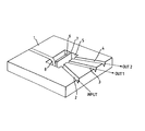
- the optical element or assembly shown in the drawing includes a substrate comprising a single crystal silicon slice 1 in the upper surface of which three V-shaped grooves 2-4 have been etched using an anisotropic masking and etching technique.
- the grooves 2-4 all have substantially the same depth and are effectively coplanar.
- Each groove 2-4 terminates in a cavity 5 formed in the substrate 1.
- Monomode optical fibres (not shown) are positioned in each of the grooves 2-4 with their ends facing into the cavity 5.
- a cantilevered, vertically hinged silicon beam 6 is positioned in the cavity 5 and is integrally formed with the remainder of the substrate 1.
- the beam 6 acts as an optical reflector.
- the beam can pivot about its end 7 between first and second positions in response to an electrostatic field generated by a pair of electrodes, one of which 8 is mounted to the substrate and the other of which is mounted to the facing surface of the beam 6. If the beam is at ground potential, the second electrode is not required.
- the electrodes are connected to electrical control apparatus including a power source (not shown).
- the reflector 6 In its first position, the reflector 6 reflects optical radiation passing along the optical fibre in the groove 2 into the optical fibre in the groove 3. In its second position, optical radiation impinging on the reflector 6 from the fibre in the groove 2 is reflected into the fibre in the groove 4.
- the element shown in the drawing can thus be used as an optical switch to switch incoming radiation in the optical fibre in the groove 2 into either the optical fibre in the groove 3 or the optical fibre in the groove 4.
Abstract
Description
- The invention relates to radiation deflector assemblies of the kind comprising at least three radiation waveguides; a controllable radiation deflector positioned such that when the deflector is in a first position radiation passes between one combination of two of the waveguides, and when the deflector is in a second position radiation passes between another combination of two of the waveguides; and control means responsive to control signals for controlling the position of the deflector. Such assembliess are hereinafter referred to as of the kind described.
- Radiation deflector assemblies of the kind described find particular application as switches in optical transmission systems. IBM Technical Disclosure Bulletin Vol 27,
No 2 of July 1984 (pages 11-12) describes a solid-state array of mirrors positioned beneath three groups of optical fibres. In a relaxed position, optical radiation impinging on the mirrors from one group of fibres is reflected towards another group. When the mirrors are in a deflected position, optical radiation is instead reflected towards the third group of fibres. - The major problem with this arrangement is that it is difficult accurately to align the optical fibres with the mirrors. Alignment is important when large arrays of mirrors are concerned so as to maximise the number of mirrors per unit area.
- In accordance with the present invention, a radiation deflector assembly of the kind described is characterised in that the waveguides and the deflector are mounted in a common substrate.
- The invention deals with the alignment problem by mounting both the waveguides and the deflector in the same substrate.
- Preferably, the waveguides are substantially coplanar, and conveniently the direction of movement of the deflector is in substantially the same plane as the plane of the waveguides. In alternative arrangements, however, the waveguides may extend in different planes.
- The invention is particularly suitable where the substrate comprises a single crystal of for example silicon, since anisotropic etching techniques may be used to define grooves of the same or different depths into which the waveguides are mounted.
- The invention is particularly suitable for deflecting radiation in the optical waveband and typically a large number of radiation deflector assemblies according to the invention will be assembled together to constitute an optical switch array.
- In some arrangements, the deflector may comprise a piston member which moves to and fro between the first and second positions. Preferably, however, the deflector comprises a cantilevered arm which is controlled to pivot between the first and second positions.
- It is particularly convenient if the deflector is integrally formed with the substrate. This can be achieved using conventional etching techniques or laser etching technology.
- Preferably, the deflector is adapted to deflect the radiation in both the first and second positions although in some examples, radiation could pass directly from. one waveguide to another when the deflector is in the first position and be deflected towards another waveguide when the deflector is in the second position.
- The deflector will typically comprise a radiation reflector but other deflectors are possible such as a refractor or diffractor.
- In some examples, the waveguides could be formed by diffusing a suitable material into the substrate but conveniently each waveguide is mounted in a groove formed in a surface of the substrate, typically a V-shaped groove.
- As has previously been mentioned, the substrate may comprise silicon but other substrate materials are possible such as silica or lithium niobate or III-V compounds such as gallium arsenide.
- The position of the deflector can be controlled using conventional electrostatic techniques or by thermal methods similar to those described in our copending British Patent Application of even date entitled "Movable Member Mounting" (our case ref: 23332/GB).
- An example of an optical reflection assembly according to the invention for use in an optical switch array will now be described with reference to the accompanying drawing which is a schematic perspective view of the assembly.
- The optical element or assembly shown in the drawing includes a substrate comprising a single
crystal silicon slice 1 in the upper surface of which three V-shaped grooves 2-4 have been etched using an anisotropic masking and etching technique. The grooves 2-4 all have substantially the same depth and are effectively coplanar. Each groove 2-4 terminates in acavity 5 formed in thesubstrate 1. Monomode optical fibres (not shown) are positioned in each of the grooves 2-4 with their ends facing into thecavity 5. - A cantilevered, vertically hinged
silicon beam 6 is positioned in thecavity 5 and is integrally formed with the remainder of thesubstrate 1. Thebeam 6 acts as an optical reflector. - The beam can pivot about its end 7 between first and second positions in response to an electrostatic field generated by a pair of electrodes, one of which 8 is mounted to the substrate and the other of which is mounted to the facing surface of the
beam 6. If the beam is at ground potential, the second electrode is not required. The electrodes are connected to electrical control apparatus including a power source (not shown). - In its first position, the
reflector 6 reflects optical radiation passing along the optical fibre in thegroove 2 into the optical fibre in thegroove 3. In its second position, optical radiation impinging on thereflector 6 from the fibre in thegroove 2 is reflected into the fibre in the groove 4. The element shown in the drawing can thus be used as an optical switch to switch incoming radiation in the optical fibre in thegroove 2 into either the optical fibre in thegroove 3 or the optical fibre in the groove 4.
Claims (10)
Priority Applications (1)
| Application Number | Priority Date | Filing Date | Title |
|---|---|---|---|
| AT86308049T ATE61487T1 (en) | 1985-10-16 | 1986-10-16 | DEFLECTION DEVICE FOR RADIATION. |
Applications Claiming Priority (12)
| Application Number | Priority Date | Filing Date | Title |
|---|---|---|---|
| GB858525460A GB8525460D0 (en) | 1985-10-16 | 1985-10-16 | Movable member mounting |
| GB858525461A GB8525461D0 (en) | 1985-10-16 | 1985-10-16 | Wavelength selection device |
| GB858525459A GB8525459D0 (en) | 1985-10-16 | 1985-10-16 | Mounting component to substrate |
| GB858525458A GB8525458D0 (en) | 1985-10-16 | 1985-10-16 | Positioning optical components & waveguides |
| GB858525462A GB8525462D0 (en) | 1985-10-16 | 1985-10-16 | Radiation deflector assembly |
| GB8525460 | 1985-10-23 | ||
| GB8525462 | 1985-10-23 | ||
| GB8525461 | 1985-10-23 | ||
| GB8526189 | 1985-10-23 | ||
| GB8525458 | 1985-10-23 | ||
| GB858526189A GB8526189D0 (en) | 1985-10-23 | 1985-10-23 | Fabry-perot interferometer |
| GB8525459 | 1985-10-23 |
Publications (2)
| Publication Number | Publication Date |
|---|---|
| EP0219358A1 true EP0219358A1 (en) | 1987-04-22 |
| EP0219358B1 EP0219358B1 (en) | 1991-03-06 |
Family
ID=27546918
Family Applications (6)
| Application Number | Title | Priority Date | Filing Date |
|---|---|---|---|
| EP86308049A Expired - Lifetime EP0219358B1 (en) | 1985-10-16 | 1986-10-16 | Radiation deflector assembly |
| EP86308047A Expired EP0219356B1 (en) | 1985-10-16 | 1986-10-16 | Movable member mounting |
| EP86308046A Expired - Lifetime EP0223414B1 (en) | 1985-10-16 | 1986-10-16 | Mounting a component to a substrate |
| EP86308048A Expired EP0219357B1 (en) | 1985-10-16 | 1986-10-16 | Wavelength selection device and method |
| EP86308050A Expired EP0219359B1 (en) | 1985-10-16 | 1986-10-16 | Fabry-perot interferometer |
| EP86308045A Expired - Lifetime EP0226296B1 (en) | 1985-10-16 | 1986-10-16 | Optical component and waveguide assembly |
Family Applications After (5)
| Application Number | Title | Priority Date | Filing Date |
|---|---|---|---|
| EP86308047A Expired EP0219356B1 (en) | 1985-10-16 | 1986-10-16 | Movable member mounting |
| EP86308046A Expired - Lifetime EP0223414B1 (en) | 1985-10-16 | 1986-10-16 | Mounting a component to a substrate |
| EP86308048A Expired EP0219357B1 (en) | 1985-10-16 | 1986-10-16 | Wavelength selection device and method |
| EP86308050A Expired EP0219359B1 (en) | 1985-10-16 | 1986-10-16 | Fabry-perot interferometer |
| EP86308045A Expired - Lifetime EP0226296B1 (en) | 1985-10-16 | 1986-10-16 | Optical component and waveguide assembly |
Country Status (9)
| Country | Link |
|---|---|
| US (7) | US4825262A (en) |
| EP (6) | EP0219358B1 (en) |
| JP (5) | JP2514343B2 (en) |
| AT (6) | ATE48480T1 (en) |
| DE (6) | DE3677881D1 (en) |
| ES (3) | ES2011773B3 (en) |
| GR (3) | GR3000242T3 (en) |
| SG (1) | SG892G (en) |
| WO (6) | WO1987002472A1 (en) |
Cited By (9)
| Publication number | Priority date | Publication date | Assignee | Title |
|---|---|---|---|---|
| DE3801764A1 (en) * | 1988-01-22 | 1989-08-03 | Ant Nachrichtentech | WAVELENGTH MULTIPLEXER OR DEMULTIPLEXER, AND METHOD FOR PRODUCING THE WAVELENGTH MULTIPLEXER OR DEMULTIPLEXER |
| EP0420468A2 (en) * | 1989-09-25 | 1991-04-03 | Hazeltine Corporation | Method and apparatus for optical signal multiplexing/demultiplexing |
| EP0525395A1 (en) * | 1991-06-28 | 1993-02-03 | Texas Instruments Incorporated | Apparatus and method for optical switching |
| FR2717581A1 (en) * | 1994-03-18 | 1995-09-22 | Sea N Optic Sa | Displacement detection device by deflection of light beam from optical fiber. |
| EP0902311A2 (en) * | 1997-09-09 | 1999-03-17 | Lucent Technologies Inc. | Article comprising a photostrictive switching element |
| EP1033601A1 (en) * | 1999-03-04 | 2000-09-06 | Japan Aviation Electronics Industry, Limited | Optical switch and method of making the same |
| EP1189092A2 (en) * | 2000-09-06 | 2002-03-20 | Japan Aviation Electronics Industry, Limited | Electrostatically operated optical switch |
| US6463190B1 (en) | 1998-10-16 | 2002-10-08 | Japan Aviation Electronics Industry Limited | Optical switch and method of making the same |
| GB2446887A (en) * | 2007-05-04 | 2008-08-27 | Zhou Rong | A 1 |
Families Citing this family (187)
| Publication number | Priority date | Publication date | Assignee | Title |
|---|---|---|---|---|
| ATE48480T1 (en) * | 1985-10-16 | 1989-12-15 | British Telecomm | MOVABLE HOUSING FOR ONE ELEMENT. |
| US4859060A (en) * | 1985-11-26 | 1989-08-22 | 501 Sharp Kabushiki Kaisha | Variable interferometric device and a process for the production of the same |
| US4744627A (en) * | 1986-11-03 | 1988-05-17 | General Electric Company | Optical fiber holder |
| GB8707854D0 (en) * | 1987-04-02 | 1987-05-07 | British Telecomm | Radiation deflector assembly |
| US4900118A (en) * | 1987-05-22 | 1990-02-13 | Furukawa Electric Co., Ltd. | Multiple-fiber optical component and method for manufacturing of the same |
| US4787696A (en) * | 1987-12-18 | 1988-11-29 | Gte Laboratories Incorporated | Mounting apparatus for optical fibers and lasers |
| GB8805015D0 (en) * | 1988-03-02 | 1988-03-30 | British Telecomm | Optical fibre locating apparatus |
| US4904036A (en) * | 1988-03-03 | 1990-02-27 | American Telephone And Telegraph Company, At&T Bell Laboratories | Subassemblies for optoelectronic hybrid integrated circuits |
| EP0331332A3 (en) * | 1988-03-03 | 1991-01-16 | AT&T Corp. | Device including a component in alignment with a substrate-supported waveguide |
| US4966433A (en) * | 1988-03-03 | 1990-10-30 | At&T Bell Laboratories | Device including a component in alignment with a substrate-supported waveguide |
| US4897711A (en) * | 1988-03-03 | 1990-01-30 | American Telephone And Telegraph Company | Subassembly for optoelectronic devices |
| US4945400A (en) * | 1988-03-03 | 1990-07-31 | At&T Bell Laboratories | Subassembly for optoelectronic devices |
| DE3809597A1 (en) * | 1988-03-22 | 1989-10-05 | Fraunhofer Ges Forschung | MICROMECHANICAL ACTUATOR |
| US4867524A (en) * | 1988-09-08 | 1989-09-19 | United Technologies Corporation | Metallic bond for mounting of optical fibers to integrated optical chips |
| EP0361153A3 (en) * | 1988-09-29 | 1991-07-24 | Siemens Aktiengesellschaft | Arrangement for coupling an optical fibre with a coupling window of a planar integrated optical device, and method for making such an arrangement |
| JPH02124504A (en) * | 1988-11-02 | 1990-05-11 | Toshiba Corp | Photodetecting module |
| US5000534A (en) * | 1988-12-05 | 1991-03-19 | Nippon Sheet Glass Co., Ltd. | Optical switch |
| US5017263A (en) * | 1988-12-23 | 1991-05-21 | At&T Bell Laboratories | Optoelectronic device package method |
| DE59010539D1 (en) * | 1989-01-09 | 1996-11-21 | Siemens Ag | Arrangement for optically coupling an optical waveguide around a photodiode on a silicon substrate |
| US4976506A (en) * | 1989-02-13 | 1990-12-11 | Pavlath George A | Methods for rugged attachment of fibers to integrated optics chips and product thereof |
| US4997253A (en) * | 1989-04-03 | 1991-03-05 | Tektronix, Inc. | Electro-optical transducer module and a method of fabricating such a module |
| US5069419A (en) * | 1989-06-23 | 1991-12-03 | Ic Sensors Inc. | Semiconductor microactuator |
| US5243673A (en) * | 1989-08-02 | 1993-09-07 | E. I. Du Pont De Nemours And Company | Opto-electronic component having positioned optical fiber associated therewith |
| GB8919220D0 (en) * | 1989-08-24 | 1989-10-04 | British Telecomm | Diffraction grating assembly |
| US5026138A (en) * | 1989-08-29 | 1991-06-25 | Gte Laboratories Incorporated | Multi-fiber alignment package for tilted facet optoelectronic components |
| DE4002490A1 (en) * | 1989-08-31 | 1991-08-01 | Bodenseewerk Geraetetech | METHOD FOR ATTACHING ELECTRO-OPTICAL COMPONENTS TO INTEGRATED-OPTICAL WAVE GUIDES |
| US5011249A (en) * | 1989-12-20 | 1991-04-30 | Raychem Corp. | Circuit for the transmission of optical signals |
| US5082242A (en) * | 1989-12-27 | 1992-01-21 | Ulrich Bonne | Electronic microvalve apparatus and fabrication |
| US5168385A (en) * | 1990-01-24 | 1992-12-01 | Canon Kabushiki Kaisha | Optical device and producing method therefor |
| US5144498A (en) * | 1990-02-14 | 1992-09-01 | Hewlett-Packard Company | Variable wavelength light filter and sensor system |
| US5042889A (en) * | 1990-04-09 | 1991-08-27 | At&T Bell Laboratories | Magnetic activation mechanism for an optical switch |
| US5195154A (en) * | 1990-04-27 | 1993-03-16 | Ngk Insulators, Ltd. | Optical surface mount technology (o-smt), optical surface mount circuit (o-smc), opto-electronic printed wiring board (oe-pwb), opto-electronic surface mount device (oe-smd), and methods of fabricating opto-electronic printed wiring board |
| US5023881A (en) * | 1990-06-19 | 1991-06-11 | At&T Bell Laboratories | Photonics module and alignment method |
| GB9014639D0 (en) * | 1990-07-02 | 1990-08-22 | British Telecomm | Optical component packaging |
| DE4022026C2 (en) * | 1990-07-11 | 1998-11-12 | Siemens Ag | Arrangement for optically coupling a laser amplifier chip to an optical fiber by means of a lens |
| US5109455A (en) * | 1990-08-03 | 1992-04-28 | Cts Corporation | Optic interface hybrid |
| US5124281A (en) * | 1990-08-27 | 1992-06-23 | At&T Bell Laboratories | Method of fabricating a photonics module comprising a spherical lens |
| US5218420A (en) * | 1991-04-11 | 1993-06-08 | The Boeing Company | Optical resonance accelerometer |
| US5142414A (en) * | 1991-04-22 | 1992-08-25 | Koehler Dale R | Electrically actuatable temporal tristimulus-color device |
| US5162872A (en) * | 1991-07-02 | 1992-11-10 | The United States Of America As Represented The Secretary Of The Air Force | Tilt/shear immune tunable fabry-perot interferometer |
| EP0522417A1 (en) * | 1991-07-09 | 1993-01-13 | Sumitomo Electric Industries, Limited | Light-receiving apparatus with optical fiber connection |
| US5586013A (en) * | 1991-07-19 | 1996-12-17 | Minnesota Mining And Manufacturing Company | Nonimaging optical illumination system |
| US5170283A (en) * | 1991-07-24 | 1992-12-08 | Northrop Corporation | Silicon spatial light modulator |
| US5173959A (en) * | 1991-09-13 | 1992-12-22 | Gte Laboratories Incorporated | Method and apparatus for assembling a fiber array |
| FR2681440B1 (en) * | 1991-09-17 | 1994-11-04 | Commissariat Energie Atomique | OPTICAL SWITCH AND MANUFACTURING METHOD THEREOF. |
| US5276756A (en) * | 1991-12-06 | 1994-01-04 | Amoco Corporation | High speed electro-optical signal translator |
| US5909280A (en) * | 1992-01-22 | 1999-06-01 | Maxam, Inc. | Method of monolithically fabricating a microspectrometer with integrated detector |
| US6147756A (en) * | 1992-01-22 | 2000-11-14 | Northeastern University | Microspectrometer with sacrificial layer integrated with integrated circuit on the same substrate |
| JPH07503328A (en) * | 1992-01-28 | 1995-04-06 | ブリテイッシュ・テレコミュニケーションズ・パブリック・リミテッド・カンパニー | Alignment of integrated optical components |
| US5280173A (en) * | 1992-01-31 | 1994-01-18 | Brown University Research Foundation | Electric and electromagnetic field sensing system including an optical transducer |
| US5208880A (en) * | 1992-04-30 | 1993-05-04 | General Electric Company | Microdynamical fiber-optic switch and method of switching using same |
| SE515191C2 (en) * | 1992-05-05 | 2001-06-25 | Volvo Ab | Process for manufacturing a pressure measuring device and pressure measuring device |
| FI98095C (en) * | 1992-05-19 | 1997-04-10 | Vaisala Technologies Inc Oy | Fabry-Perot resonator based optical force sensor with sweeping Fabry-Perot resonator as part of the detector |
| NL9200884A (en) * | 1992-05-20 | 1993-12-16 | Framatome Connectors Belgium | CONNECTOR ASSEMBLY. |
| US5271597A (en) * | 1992-05-29 | 1993-12-21 | Ic Sensors, Inc. | Bimetallic diaphragm with split hinge for microactuator |
| US5253311A (en) * | 1992-11-02 | 1993-10-12 | The United States Of America As Represented By The Secretary Of The Army | Device and method for performing optical coupling without pigtails |
| US5343548A (en) * | 1992-12-15 | 1994-08-30 | International Business Machines Corporation | Method and apparatus for batch, active alignment of laser arrays to fiber arrays |
| DE4301236C1 (en) * | 1993-01-19 | 1994-03-17 | Ant Nachrichtentech | Optical fibre coupling to opto-electrical transducer, e.g. photodiode - supports transducer parallel to angled end face of optical fibre at end of V-shaped reception groove for latter |
| GB2275787A (en) * | 1993-03-05 | 1994-09-07 | British Aerospace | Silicon micro-mirror unit |
| JP2842132B2 (en) * | 1993-03-05 | 1998-12-24 | 松下電器産業株式会社 | Optical device |
| US5457573A (en) * | 1993-03-10 | 1995-10-10 | Matsushita Electric Industrial Co., Ltd. | Diffraction element and an optical multiplexing/demultiplexing device incorporating the same |
| JPH06334262A (en) * | 1993-03-23 | 1994-12-02 | Mitsubishi Electric Corp | Semiconductor laser array device, semiconductor laser device, and their manufacture |
| US5343542A (en) * | 1993-04-22 | 1994-08-30 | International Business Machines Corporation | Tapered fabry-perot waveguide optical demultiplexer |
| DE4320194A1 (en) * | 1993-06-18 | 1994-12-22 | Sel Alcatel Ag | Device for the adjustment-free coupling of a plurality of optical fibers to a laser array |
| US5345521A (en) * | 1993-07-12 | 1994-09-06 | Texas Instrument Incorporated | Architecture for optical switch |
| GB2280544B (en) * | 1993-07-30 | 1997-01-08 | Northern Telecom Ltd | Providing optical coupling with single crystal substrate mounted electro-optic transducers |
| JP3302458B2 (en) * | 1993-08-31 | 2002-07-15 | 富士通株式会社 | Integrated optical device and manufacturing method |
| DE4334578C2 (en) * | 1993-10-11 | 1999-10-07 | Dirk Winfried Rossberg | Spectrally tunable infrared sensor |
| US6012855A (en) * | 1993-11-09 | 2000-01-11 | Hewlett-Packard Co. | Method and apparatus for parallel optical data link |
| US5500761A (en) * | 1994-01-27 | 1996-03-19 | At&T Corp. | Micromechanical modulator |
| SE503905C2 (en) * | 1994-03-16 | 1996-09-30 | Ericsson Telefon Ab L M | Process for producing an optocomponent and an optocomponent |
| SE513183C2 (en) * | 1994-03-18 | 2000-07-24 | Ericsson Telefon Ab L M | Process for producing an optocomponent and nested optocomponent |
| US7826120B2 (en) * | 1994-05-05 | 2010-11-02 | Qualcomm Mems Technologies, Inc. | Method and device for multi-color interferometric modulation |
| US7839556B2 (en) * | 1994-05-05 | 2010-11-23 | Qualcomm Mems Technologies, Inc. | Method and device for modulating light |
| DE4431285C1 (en) * | 1994-09-02 | 1995-12-07 | Ant Nachrichtentech | Semiconductor laser module esp. for coupling into optical waveguide |
| US5553182A (en) * | 1995-02-14 | 1996-09-03 | Mcdonnell Douglas Corporation | Alignment fixture and associated method for controllably positioning on optical fiber |
| US7898722B2 (en) * | 1995-05-01 | 2011-03-01 | Qualcomm Mems Technologies, Inc. | Microelectromechanical device with restoring electrode |
| US5606635A (en) * | 1995-06-07 | 1997-02-25 | Mcdonnell Douglas Corporation | Fiber optic connector having at least one microactuator for precisely aligning an optical fiber and an associated fabrication method |
| US5602955A (en) * | 1995-06-07 | 1997-02-11 | Mcdonnell Douglas Corporation | Microactuator for precisely aligning an optical fiber and an associated fabrication method |
| WO1998012587A1 (en) * | 1995-06-07 | 1998-03-26 | Mcdonnell Douglas Corporation | An alignment apparatus for precisely aligning an optical fiber and an associated fabrication method |
| DE69618035T2 (en) * | 1995-06-30 | 2002-07-11 | Whitaker Corp | DEVICE FOR ALIGNING AN OPTOELECTRONIC COMPONENT |
| US6324192B1 (en) | 1995-09-29 | 2001-11-27 | Coretek, Inc. | Electrically tunable fabry-perot structure utilizing a deformable multi-layer mirror and method of making the same |
| GB9521100D0 (en) * | 1995-10-16 | 1995-12-20 | Hewlett Packard Ltd | Optical connector |
| FR2740550B1 (en) * | 1995-10-27 | 1997-12-12 | Schlumberger Ind Sa | FILTER FOR ELECTROMAGNETIC RADIATION AND DEVICE FOR DETERMINING A CONCENTRATION OF GAS COMPRISING SUCH A FILTER |
| US5659647A (en) * | 1995-10-30 | 1997-08-19 | Sandia Corporation | Fiber alignment apparatus and method |
| US7907319B2 (en) * | 1995-11-06 | 2011-03-15 | Qualcomm Mems Technologies, Inc. | Method and device for modulating light with optical compensation |
| SE512121C2 (en) * | 1995-12-19 | 2000-01-31 | Ericsson Telefon Ab L M | A method of passively aligning a waveguide on a substrate |
| US5659641A (en) | 1995-12-22 | 1997-08-19 | Corning, Inc. | Optical circuit on printed circuit board |
| US5872880A (en) * | 1996-08-12 | 1999-02-16 | Ronald S. Maynard | Hybrid-optical multi-axis beam steering apparatus |
| US5862283A (en) * | 1996-08-28 | 1999-01-19 | Hewlett-Packard Company | Mounting a planar optical component on a mounting member |
| DE69630956T2 (en) * | 1996-10-17 | 2004-10-21 | British Telecomm | Tunable optical filter |
| US7830588B2 (en) * | 1996-12-19 | 2010-11-09 | Qualcomm Mems Technologies, Inc. | Method of making a light modulating display device and associated transistor circuitry and structures thereof |
| US5940558A (en) * | 1997-01-02 | 1999-08-17 | Lucent Technologies, Inc. | Optical packaging assembly for transmissive devices |
| IT1288435B1 (en) * | 1997-01-28 | 1998-09-22 | Pirelli | TIRE AND TREAD BAND FOR TIRES PARTICULARLY FOR TRUCKS AND SIMILAR |
| US5970200A (en) * | 1997-03-21 | 1999-10-19 | Kabushiki Kaisha Toshiba | Apparatus having optical components and a manufacturing method thereof |
| US5896481A (en) * | 1997-05-30 | 1999-04-20 | The Boeing Company | Optical subassembly with a groove for aligning an optical device with an optical fiber |
| US5994700A (en) * | 1997-09-04 | 1999-11-30 | Lockheed Martin Energy Research Corporation | FTIR spectrometer with solid-state drive system |
| FR2768812B1 (en) * | 1997-09-19 | 1999-10-22 | Commissariat Energie Atomique | FABRY-PEROT INTERFEROMETER TUNABLE INTEGRATED |
| AU764799B2 (en) | 1997-12-29 | 2003-08-28 | Coretek, Inc. | Microelectromechanically tunable, confocal, vertical cavity surface emitting laser and fabry-perot filter |
| US6438149B1 (en) | 1998-06-26 | 2002-08-20 | Coretek, Inc. | Microelectromechanically tunable, confocal, vertical cavity surface emitting laser and fabry-perot filter |
| EP1058859A1 (en) | 1998-02-23 | 2000-12-13 | Huber & Suhner Ag | Positioning system for positioning and attaching optical fibres and connectors provided with this positioning system |
| US5981975A (en) * | 1998-02-27 | 1999-11-09 | The Whitaker Corporation | On-chip alignment fiducials for surface emitting devices |
| US6085007A (en) * | 1998-02-27 | 2000-07-04 | Jiang; Ching-Long | Passive alignment member for vertical surface emitting/detecting device |
| SE513858C2 (en) | 1998-03-06 | 2000-11-13 | Ericsson Telefon Ab L M | Multilayer structure and method of manufacturing multilayer modules |
| US6095697A (en) * | 1998-03-31 | 2000-08-01 | Honeywell International Inc. | Chip-to-interface alignment |
| KR100703140B1 (en) | 1998-04-08 | 2007-04-05 | 이리다임 디스플레이 코포레이션 | Interferometric modulation and its manufacturing method |
| US8928967B2 (en) * | 1998-04-08 | 2015-01-06 | Qualcomm Mems Technologies, Inc. | Method and device for modulating light |
| FI116753B (en) * | 1998-04-17 | 2006-02-15 | Valtion Teknillinen | Wavelength adjustable laser arrangement |
| US6584126B2 (en) | 1998-06-26 | 2003-06-24 | Coretek, Inc. | Tunable Fabry-Perot filter and tunable vertical cavity surface emitting laser |
| US6813291B2 (en) | 1998-06-26 | 2004-11-02 | Coretek Inc | Tunable fabry-perot filter and tunable vertical cavity surface emitting laser |
| US6585427B2 (en) | 1999-01-11 | 2003-07-01 | Intel Corporation | Flexure coupled to a substrate for maintaining the optical fibers in alignment |
| US6227724B1 (en) * | 1999-01-11 | 2001-05-08 | Lightlogic, Inc. | Method for constructing an optoelectronic assembly |
| US6207950B1 (en) | 1999-01-11 | 2001-03-27 | Lightlogic, Inc. | Optical electronic assembly having a flexure for maintaining alignment between optical elements |
| DE19902184C1 (en) * | 1999-01-21 | 2000-09-21 | Winter & Ibe Olympus | Medical endoscope for viewing fluorescent marked areas |
| US6742774B2 (en) | 1999-07-02 | 2004-06-01 | Holl Technologies Company | Process for high shear gas-liquid reactions |
| US6471392B1 (en) | 2001-03-07 | 2002-10-29 | Holl Technologies Company | Methods and apparatus for materials processing |
| US7538237B2 (en) | 1999-07-02 | 2009-05-26 | Kreido Laboratories | Process for high shear gas-liquid reactions |
| WO2003007049A1 (en) | 1999-10-05 | 2003-01-23 | Iridigm Display Corporation | Photonic mems and structures |
| DE19955759A1 (en) * | 1999-11-20 | 2001-05-23 | Colour Control Farbmestechnik | Monochromator; has fixed spatial filter to limit solid angle of incident light, dispersion prism and monolithic micromechanical tilting mirror to control geometrical solid angle variation of radiation |
| US6295130B1 (en) * | 1999-12-22 | 2001-09-25 | Xerox Corporation | Structure and method for a microelectromechanically tunable fabry-perot cavity spectrophotometer |
| US6711321B2 (en) | 2000-01-20 | 2004-03-23 | Japan Science And Technology Corporation | Mechanical optical switch and method for manufacturing the same |
| US6836366B1 (en) * | 2000-03-03 | 2004-12-28 | Axsun Technologies, Inc. | Integrated tunable fabry-perot filter and method of making same |
| US6597461B1 (en) | 2000-03-20 | 2003-07-22 | Parvenu, Inc. | Tunable fabry-perot interferometer using entropic materials |
| US6665109B2 (en) | 2000-03-20 | 2003-12-16 | Np Photonics, Inc. | Compliant mechanism and method of forming same |
| US6747775B2 (en) * | 2000-03-20 | 2004-06-08 | Np Photonics, Inc. | Detunable Fabry-Perot interferometer and an add/drop multiplexer using the same |
| US6678084B2 (en) | 2000-03-20 | 2004-01-13 | Np Photonics, Inc. | Methods of making mechanisms in which relative locations of elements are maintained during manufacturing |
| US6519074B2 (en) | 2000-03-20 | 2003-02-11 | Parvenu, Inc. | Electrostatically-actuated tunable optical components using entropic materials |
| US6747784B2 (en) | 2000-03-20 | 2004-06-08 | Np Photonics, Inc. | Compliant mechanism and method of forming same |
| US6738145B2 (en) | 2000-04-14 | 2004-05-18 | Shipley Company, L.L.C. | Micromachined, etalon-based optical fiber pressure sensor |
| NL1015131C1 (en) | 2000-04-16 | 2001-10-19 | Tmp Total Micro Products B V | Apparatus and method for switching electromagnetic signals or beams. |
| US6496616B2 (en) | 2000-04-28 | 2002-12-17 | Confluent Photonics, Inc. | Miniature monolithic optical demultiplexer |
| US6453087B2 (en) | 2000-04-28 | 2002-09-17 | Confluent Photonics Co. | Miniature monolithic optical add-drop multiplexer |
| US6768590B2 (en) * | 2000-05-19 | 2004-07-27 | Shipley Company, L.L.C. | Method of fabricating optical filters |
| WO2002010836A2 (en) * | 2000-07-27 | 2002-02-07 | Holl Technologies, Inc. | Flexureless magnetic micromirror assembly |
| CA2314783A1 (en) * | 2000-08-01 | 2002-02-01 | Kenneth Lloyd Westra | A method of making a high reflectivity micro mirror and a micro mirror |
| US6810176B2 (en) | 2000-08-07 | 2004-10-26 | Rosemount Inc. | Integrated transparent substrate and diffractive optical element |
| US7003187B2 (en) | 2000-08-07 | 2006-02-21 | Rosemount Inc. | Optical switch with moveable holographic optical element |
| KR100361593B1 (en) * | 2000-11-23 | 2002-11-22 | 주식회사일진 | Optical integrated circuit device having protrusion, fabrication method of the same and module of optical communication transmission and receiving apparatus using the same |
| DE10061765A1 (en) * | 2000-12-12 | 2003-03-06 | Colour Control Farbmestechnik | Micromechanical monochromator with integrated aperture stop has at least one of its aperture stops as constituent of monolithic body of micromechanical torsion diffraction grid |
| US6516131B1 (en) | 2001-04-04 | 2003-02-04 | Barclay J. Tullis | Structures and methods for aligning fibers |
| US6830806B2 (en) | 2001-04-12 | 2004-12-14 | Kreido Laboratories | Methods of manufacture of electric circuit substrates and components having multiple electric characteristics and substrates and components so manufactured |
| US6965721B1 (en) * | 2001-04-18 | 2005-11-15 | Tullis Barclay J | Integrated manufacture of side-polished fiber optics |
| JP4720022B2 (en) * | 2001-05-30 | 2011-07-13 | ソニー株式会社 | OPTICAL MULTILAYER STRUCTURE, ITS MANUFACTURING METHOD, OPTICAL SWITCHING DEVICE, AND IMAGE DISPLAY DEVICE |
| US6618519B2 (en) * | 2001-07-16 | 2003-09-09 | Chromux Technologies, Inc. | Switch and variable optical attenuator for single or arrayed optical channels |
| US6787246B2 (en) | 2001-10-05 | 2004-09-07 | Kreido Laboratories | Manufacture of flat surfaced composites comprising powdered fillers in a polymer matrix |
| US6658032B2 (en) | 2001-10-05 | 2003-12-02 | Pranalytica, Inc. | Automated laser wavelength selection system and method |
| NO315177B1 (en) | 2001-11-29 | 2003-07-21 | Sinvent As | Optical offset sensor |
| US6775436B1 (en) | 2002-02-26 | 2004-08-10 | General Dynamics Advanced Technology Systems, Inc. | Optical fiber U-turn apparatus and method |
| US6987901B2 (en) * | 2002-03-01 | 2006-01-17 | Rosemount, Inc. | Optical switch with 3D waveguides |
| AU2003258781A1 (en) * | 2002-03-29 | 2003-10-13 | Massachusetts Institute Of Technology | Low voltage tunable filtre with photonic crystal |
| US6869231B2 (en) * | 2002-05-01 | 2005-03-22 | Jds Uniphase Corporation | Transmitters, receivers, and transceivers including an optical bench |
| WO2003098302A2 (en) * | 2002-05-15 | 2003-11-27 | Hymite A/S | Optical device receiving substrate and optical device holding carrier |
| JP2003344709A (en) * | 2002-05-23 | 2003-12-03 | Okano Electric Wire Co Ltd | Fiber type optical module |
| JP3801099B2 (en) * | 2002-06-04 | 2006-07-26 | 株式会社デンソー | Tunable filter, manufacturing method thereof, and optical switching device using the same |
| US7098360B2 (en) | 2002-07-16 | 2006-08-29 | Kreido Laboratories | Processes employing multiple successive chemical reaction process steps and apparatus therefore |
| BR0314521A (en) | 2002-09-11 | 2005-07-26 | Kreido Lab | Methods and devices for high shear material mixers and reactors |
| WO2004030802A2 (en) | 2002-10-03 | 2004-04-15 | Kreido Laboratories | Apparatus for transfer of heat energy between a body surface and heat transfer fluid |
| DE10248924A1 (en) * | 2002-10-17 | 2004-04-29 | C. & E. Fein Gmbh & Co Kg | power tool |
| US6996312B2 (en) * | 2003-04-29 | 2006-02-07 | Rosemount, Inc. | Tunable fabry-perot filter |
| JP4916647B2 (en) * | 2003-05-23 | 2012-04-18 | サムスン エレクトロニクス カンパニー リミテッド | External cavity semiconductor laser and manufacturing method thereof |
| US20050201668A1 (en) * | 2004-03-11 | 2005-09-15 | Avi Neta | Method of connecting an optical element at a slope |
| US7187453B2 (en) * | 2004-04-23 | 2007-03-06 | Opsens Inc. | Optical MEMS cavity having a wide scanning range for measuring a sensing interferometer |
| JP3985269B2 (en) * | 2004-09-29 | 2007-10-03 | 松下電工株式会社 | Light switch |
| NO20051850A (en) | 2005-04-15 | 2006-09-25 | Sinvent As | Infrared detection of gas - diffractive. |
| US7916980B2 (en) | 2006-01-13 | 2011-03-29 | Qualcomm Mems Technologies, Inc. | Interconnect structure for MEMS device |
| US7480432B2 (en) | 2006-02-28 | 2009-01-20 | Corning Incorporated | Glass-based micropositioning systems and methods |
| WO2007126475A2 (en) * | 2006-04-26 | 2007-11-08 | Davidson Instruments, Inc. | Fiber optic mems seismic sensor with mass supported by hinged beams |
| US20080049228A1 (en) * | 2006-08-28 | 2008-02-28 | Novaspectra, Inc. | Fabry-perot interferometer array |
| JP2009003096A (en) * | 2007-06-20 | 2009-01-08 | Sumitomo Bakelite Co Ltd | Optical waveguide module and manufacturing method of the same |
| DE102008051625B4 (en) | 2008-10-02 | 2015-08-13 | Erich Kasper | Method for producing a component with an optical coupling window |
| US8036508B2 (en) | 2009-09-21 | 2011-10-11 | Corning Incorporated | Methods for passively aligning opto-electronic component assemblies on substrates |
| CN102384809B (en) * | 2011-08-09 | 2013-05-08 | 天津大学 | High-stability optical fiber Fabry-Perot pressure sensor packaged without glue and manufacturing method |
| JP5987573B2 (en) | 2012-09-12 | 2016-09-07 | セイコーエプソン株式会社 | Optical module, electronic device, and driving method |
| CN103984062B (en) * | 2013-02-08 | 2015-10-14 | 源杰科技股份有限公司 | The packaging technology of optical-electric module and optical-electric module |
| CN103457144A (en) * | 2013-09-10 | 2013-12-18 | 中国科学院国家授时中心 | Adjustable high-stable F-P integrated endoscope device |
| JP6052269B2 (en) * | 2014-12-08 | 2016-12-27 | セイコーエプソン株式会社 | Tunable filter |
| JP6685701B2 (en) * | 2014-12-26 | 2020-04-22 | キヤノン株式会社 | Surface emitting laser, information acquisition device, imaging device, laser array, and method for manufacturing surface emitting laser |
| US9810594B2 (en) | 2015-01-08 | 2017-11-07 | Kulite Semiconductor Products, Inc. | Thermally stable high temperature pressure and acceleration optical interferometric sensors |
| US9952067B2 (en) | 2015-05-06 | 2018-04-24 | Kulite Semiconductor Products, Inc. | Systems and methods for optical measurements using multiple beam interferometric sensors |
| JP6576092B2 (en) | 2015-04-30 | 2019-09-18 | キヤノン株式会社 | Surface emitting laser, information acquisition device, and imaging device |
| JP6510990B2 (en) * | 2016-01-29 | 2019-05-08 | 浜松ホトニクス株式会社 | Wavelength variable light source and driving method thereof |
| IL253799B (en) | 2017-08-02 | 2018-06-28 | Igal Igor Zlochin | Retro-reflective interferometer |
| US10310197B1 (en) * | 2018-09-17 | 2019-06-04 | Waymo Llc | Transmitter devices having bridge structures |
| US10534143B1 (en) * | 2018-09-20 | 2020-01-14 | Waymo Llc | Methods for optical system manufacturing |
| US11226457B2 (en) * | 2020-05-28 | 2022-01-18 | Cisco Technology, Inc. | Laser and photonic chip integration |
| US11957804B2 (en) * | 2020-09-28 | 2024-04-16 | The Boeing Company | Optical disinfection systems having side-emitting optical fiber coupled to high-energy UV-C laser diode |
| GB202017243D0 (en) | 2020-10-30 | 2020-12-16 | Npl Management Ltd | Chip assembly and method of making a chip assembly |
Citations (1)
| Publication number | Priority date | Publication date | Assignee | Title |
|---|---|---|---|---|
| US4182544A (en) * | 1978-08-03 | 1980-01-08 | Sperry Rand Corporation | Resonant multiplexer-demultiplexer for optical data communication systems |
Family Cites Families (59)
| Publication number | Priority date | Publication date | Assignee | Title |
|---|---|---|---|---|
| US1438974A (en) * | 1920-11-13 | 1922-12-19 | Western Electric Co | Piezo-electrical voltage indicator |
| US2586531A (en) * | 1950-04-20 | 1952-02-19 | Donald L Gordon | Wheeled support having ladder assembly |
| US2920529A (en) * | 1952-05-23 | 1960-01-12 | Blythe Richard | Electronic control of optical and near-optical radiation |
| US3040583A (en) * | 1959-12-10 | 1962-06-26 | United Aircraft Corp | Optical pressure transducer |
| US3387531A (en) * | 1964-11-05 | 1968-06-11 | Zeiss Jena Veb Carl | Devices for supporting, adjusting and displacing at least one of two optical plates located according to the fabry-perot principle |
| US3443243A (en) * | 1965-06-23 | 1969-05-06 | Bell Telephone Labor Inc | Frequency selective laser |
| US3635562A (en) * | 1968-11-12 | 1972-01-18 | Comp Generale Electricite | Optical interferometer for detection of small displacements |
| US3704996A (en) * | 1969-10-23 | 1972-12-05 | Licentia Gmbh | Optical coupling arrangement |
| DE2242438A1 (en) * | 1972-08-29 | 1974-03-07 | Battelle Institut E V | INFRARED MODULATOR |
| FR2359433A1 (en) * | 1976-07-23 | 1978-02-17 | Thomson Csf | ADJUSTABLE RADIATION DISTRIBUTOR GUIDED BY OPTICAL FIBER BEAMS |
| US4169001A (en) * | 1976-10-18 | 1979-09-25 | International Business Machines Corporation | Method of making multilayer module having optical channels therein |
| US4070516A (en) * | 1976-10-18 | 1978-01-24 | International Business Machines Corporation | Multilayer module having optical channels therein |
| US4115747A (en) * | 1976-12-27 | 1978-09-19 | Heihachi Sato | Optical modulator using a controllable diffraction grating |
| FR2426347A1 (en) * | 1978-05-18 | 1979-12-14 | Thomson Csf | SEMICONDUCTOR LASER SOURCE AND ITS MANUFACTURING PROCESS |
| US4210923A (en) * | 1979-01-02 | 1980-07-01 | Bell Telephone Laboratories, Incorporated | Edge illuminated photodetector with optical fiber alignment |
| JPS5596903A (en) * | 1979-01-17 | 1980-07-23 | Mitsubishi Electric Corp | Photo switch |
| US4268113A (en) * | 1979-04-16 | 1981-05-19 | International Business Machines Corporation | Signal coupling element for substrate-mounted optical transducers |
| JPS56126818A (en) * | 1980-03-12 | 1981-10-05 | Nippon Telegr & Teleph Corp <Ntt> | Fine adjustment method of optical fiber axis aligning position |
| US4317611A (en) * | 1980-05-19 | 1982-03-02 | International Business Machines Corporation | Optical ray deflection apparatus |
| JPS575005A (en) * | 1980-06-12 | 1982-01-11 | Matsushita Electric Ind Co Ltd | Optical branching filter |
| JPS577989A (en) * | 1980-06-17 | 1982-01-16 | Matsushita Electric Ind Co Ltd | Mount for semiconductor laser |
| US4356730A (en) * | 1981-01-08 | 1982-11-02 | International Business Machines Corporation | Electrostatically deformographic switches |
| JPS57119314A (en) * | 1981-01-16 | 1982-07-24 | Omron Tateisi Electronics Co | Connecting method between optical fiber and optical waveguide |
| JPS57172309A (en) * | 1981-04-16 | 1982-10-23 | Omron Tateisi Electronics Co | Coupling method of optical fiber and optical waveguide |
| JPS5821832A (en) * | 1981-07-31 | 1983-02-08 | Toshiba Corp | Apparatus for supplying semiconductor part |
| DE3138296A1 (en) * | 1981-09-25 | 1983-04-28 | Siemens AG, 1000 Berlin und 8000 München | METHOD FOR POSITIONING AND FIXING OPTICAL COMPONENTS RELATIVELY TO OTHER |
| DE3142918A1 (en) * | 1981-10-29 | 1983-05-11 | Licentia Patent-Verwaltungs-Gmbh, 6000 Frankfurt | OPTO-ELECTRICAL COUPLING |
| DE3206919A1 (en) * | 1982-02-26 | 1983-09-15 | Philips Patentverwaltung Gmbh, 2000 Hamburg | DEVICE FOR OPTICALLY DISCONNECTING AND CONNECTING LIGHT GUIDES |
| US4466696A (en) * | 1982-03-29 | 1984-08-21 | Honeywell Inc. | Self-aligned coupling of optical fiber to semiconductor laser or LED |
| SE435760B (en) * | 1982-04-21 | 1984-10-15 | Asea Ab | FIBER OPTICAL GENDER |
| US4450563A (en) * | 1982-04-23 | 1984-05-22 | Westinghouse Electric Corp. | Rapidly turnable laser system |
| GB2127987B (en) * | 1982-09-29 | 1986-09-03 | Standard Telephones Cables Ltd | Integrated optic devices |
| US4468084A (en) * | 1982-11-22 | 1984-08-28 | Honeywell Inc. | Integrated optical time integrating correlator |
| US4611884A (en) * | 1982-11-24 | 1986-09-16 | Magnetic Controls Company | Bi-directional optical fiber coupler |
| FR2536867B1 (en) * | 1982-11-30 | 1986-02-07 | Thomson Csf | METHOD FOR ALIGNING AN OPTOELECTRONIC DEVICE |
| US4669817A (en) * | 1983-02-04 | 1987-06-02 | Kei Mori | Apparatus for time-sharing light distribution |
| DE3307669A1 (en) * | 1983-03-04 | 1984-09-06 | Licentia Patent-Verwaltungs-Gmbh, 6000 Frankfurt | Coupling arrangement between an electrooptical and/or optoelectric semiconductor component and an optical fibre |
| JPS59172787A (en) * | 1983-03-22 | 1984-09-29 | Sharp Corp | Submounting device for semiconductor laser |
| US4668093A (en) * | 1983-06-13 | 1987-05-26 | Mcdonnell Douglas Corporation | Optical grating demodulator and sensor system |
| DE3321988A1 (en) * | 1983-06-18 | 1984-12-20 | Standard Elektrik Lorenz Ag, 7000 Stuttgart | DEVICE FOR THE GAME-FREE MOVEMENT OF OBJECTS IN A COORDINATE SYSTEM |
| FR2549243B1 (en) * | 1983-06-24 | 1986-01-10 | Lyonnaise Transmiss Optiques | DIRECT COUPLER WITH ASSOCIATED COMPONENTS FOR LIGHT WAVE |
| JPS60107532A (en) * | 1983-11-17 | 1985-06-13 | Toshiba Corp | Multiwavelength spectrophotometer |
| CA1267468A (en) * | 1983-11-21 | 1990-04-03 | Hideaki Nishizawa | Optical device package |
| DE3404613A1 (en) * | 1984-02-09 | 1985-08-14 | Siemens AG, 1000 Berlin und 8000 München | DEVICE FOR DETACHABLE COUPLING A LIGHT WAVE GUIDE TO AN OPTOELECTRONIC COMPONENT |
| JPS60182403A (en) * | 1984-02-29 | 1985-09-18 | Sumitomo Metal Mining Co Ltd | Optical demultiplexing element |
| JPS60257413A (en) * | 1984-06-04 | 1985-12-19 | Matsushita Electric Ind Co Ltd | Photoelectric composite apparatus |
| CA1255382A (en) * | 1984-08-10 | 1989-06-06 | Masao Kawachi | Hybrid optical integrated circuit with alignment guides |
| JPS6183515A (en) * | 1984-09-18 | 1986-04-28 | Honda Motor Co Ltd | Light guide circuit unit |
| EP0175936B1 (en) * | 1984-09-24 | 1988-11-09 | Siemens Aktiengesellschaft | Opto-electronic device |
| JPS6187438A (en) * | 1984-10-04 | 1986-05-02 | Mitsubishi Electric Corp | Optical signal trolley device |
| JPS6170828U (en) * | 1984-10-16 | 1986-05-14 | ||
| US4705349A (en) * | 1985-01-18 | 1987-11-10 | The United States Of America As Represented By The United States Department Of Energy | Optical switch |
| US4699449A (en) * | 1985-03-05 | 1987-10-13 | Canadian Patents And Development Limited-Societe Canadienne Des Brevets Et D'exploitation Limitee | Optoelectronic assembly and method of making the same |
| GB8522316D0 (en) * | 1985-09-09 | 1985-10-16 | British Telecomm | Optical fibre termination |
| ATE48480T1 (en) * | 1985-10-16 | 1989-12-15 | British Telecomm | MOVABLE HOUSING FOR ONE ELEMENT. |
| US4779946A (en) * | 1986-02-14 | 1988-10-25 | American Telephone And Telegraph Company, At&T Bell Laboratories | Microminiature optical assembly |
| US4820013A (en) * | 1987-01-06 | 1989-04-11 | Alps Electric Co., Ltd. | LED array head |
| US4826272A (en) * | 1987-08-27 | 1989-05-02 | American Telephone And Telegraph Company At&T Bell Laboratories | Means for coupling an optical fiber to an opto-electronic device |
| JPH06180207A (en) * | 1992-12-11 | 1994-06-28 | Sankyo Seiki Mfg Co Ltd | Rotary angle detector |
-
1986
- 1986-10-16 AT AT86308047T patent/ATE48480T1/en not_active IP Right Cessation
- 1986-10-16 AT AT86308045T patent/ATE82076T1/en active
- 1986-10-16 US US07/080,468 patent/US4825262A/en not_active Expired - Lifetime
- 1986-10-16 WO PCT/GB1986/000628 patent/WO1987002472A1/en unknown
- 1986-10-16 EP EP86308049A patent/EP0219358B1/en not_active Expired - Lifetime
- 1986-10-16 JP JP61505474A patent/JP2514343B2/en not_active Expired - Lifetime
- 1986-10-16 DE DE8686308049T patent/DE3677881D1/en not_active Expired - Fee Related
- 1986-10-16 DE DE86308046T patent/DE3689537T2/en not_active Expired - Fee Related
- 1986-10-16 DE DE8686308045T patent/DE3687063T2/en not_active Expired - Fee Related
- 1986-10-16 WO PCT/GB1986/000629 patent/WO1987002476A1/en unknown
- 1986-10-16 AT AT86308049T patent/ATE61487T1/en active
- 1986-10-16 US US07/080,465 patent/US4854658A/en not_active Expired - Fee Related
- 1986-10-16 US US07/080,467 patent/US4802727A/en not_active Expired - Fee Related
- 1986-10-16 ES ES86308048T patent/ES2011773B3/en not_active Expired - Lifetime
- 1986-10-16 ES ES86308047T patent/ES2012346B3/en not_active Expired - Lifetime
- 1986-10-16 US US07/080,464 patent/US4867532A/en not_active Expired - Lifetime
- 1986-10-16 WO PCT/GB1986/000627 patent/WO1987002518A1/en unknown
- 1986-10-16 EP EP86308047A patent/EP0219356B1/en not_active Expired
- 1986-10-16 ES ES86308050T patent/ES2013599B3/en not_active Expired - Lifetime
- 1986-10-16 EP EP86308046A patent/EP0223414B1/en not_active Expired - Lifetime
- 1986-10-16 JP JP61505472A patent/JPH077149B2/en not_active Expired - Lifetime
- 1986-10-16 US US07/080,564 patent/US4846930A/en not_active Expired - Fee Related
- 1986-10-16 EP EP86308048A patent/EP0219357B1/en not_active Expired
- 1986-10-16 DE DE8686308047T patent/DE3667335D1/en not_active Expired - Lifetime
- 1986-10-16 AT AT86308046T patent/ATE100245T1/en not_active IP Right Cessation
- 1986-10-16 WO PCT/GB1986/000631 patent/WO1987002470A1/en unknown
- 1986-10-16 DE DE8686308050T patent/DE3669401D1/en not_active Expired - Fee Related
- 1986-10-16 WO PCT/GB1986/000630 patent/WO1987002475A1/en unknown
- 1986-10-16 DE DE8686308048T patent/DE3667864D1/en not_active Expired - Fee Related
- 1986-10-16 JP JP61505412A patent/JPH0827432B2/en not_active Expired - Lifetime
- 1986-10-16 JP JP61505413A patent/JPH0769520B2/en not_active Expired - Lifetime
- 1986-10-16 WO PCT/GB1986/000626 patent/WO1987002474A1/en unknown
- 1986-10-16 JP JP61505411A patent/JPH0690329B2/en not_active Expired - Fee Related
- 1986-10-16 AT AT86308048T patent/ATE49064T1/en not_active IP Right Cessation
- 1986-10-16 AT AT86308050T patent/ATE50864T1/en not_active IP Right Cessation
- 1986-10-16 EP EP86308050A patent/EP0219359B1/en not_active Expired
- 1986-10-16 EP EP86308045A patent/EP0226296B1/en not_active Expired - Lifetime
- 1986-10-16 US US07/080,469 patent/US4871244A/en not_active Expired - Lifetime
-
1989
- 1989-01-30 US US07/303,275 patent/US4896936A/en not_active Expired - Lifetime
- 1989-12-07 GR GR89400264T patent/GR3000242T3/en unknown
- 1989-12-28 GR GR89400280T patent/GR3000264T3/en unknown
-
1990
- 1990-03-08 GR GR90400119T patent/GR3000376T3/en unknown
-
1992
- 1992-01-07 SG SG8/92A patent/SG892G/en unknown
Patent Citations (1)
| Publication number | Priority date | Publication date | Assignee | Title |
|---|---|---|---|---|
| US4182544A (en) * | 1978-08-03 | 1980-01-08 | Sperry Rand Corporation | Resonant multiplexer-demultiplexer for optical data communication systems |
Non-Patent Citations (2)
| Title |
|---|
| IBM JOURNAL OF RESEARCH AND DEVELOPMENT, vol. 24, no. 5, September 1980, pages 631-637, Armonk, New York, US; K.E. PETERSEN: "Silicon torsional scanning mirror" * |
| IEEE TRANSACTIONS ON MICROWAVE THEORY AND TECHNIQUES, vol. MTT-30, no. 10, October 1982, pages 1572-1576, IEEE, New York, US; M.B. SPITZER et al.: "Development of an electrostatically bonded fiber optic connection technique" * |
Cited By (14)
| Publication number | Priority date | Publication date | Assignee | Title |
|---|---|---|---|---|
| DE3801764A1 (en) * | 1988-01-22 | 1989-08-03 | Ant Nachrichtentech | WAVELENGTH MULTIPLEXER OR DEMULTIPLEXER, AND METHOD FOR PRODUCING THE WAVELENGTH MULTIPLEXER OR DEMULTIPLEXER |
| EP0420468A2 (en) * | 1989-09-25 | 1991-04-03 | Hazeltine Corporation | Method and apparatus for optical signal multiplexing/demultiplexing |
| EP0420468A3 (en) * | 1989-09-25 | 1992-03-18 | Hazeltine Corporation | Method and apparatus for optical signal multiplexing/demultiplexing |
| EP0525395A1 (en) * | 1991-06-28 | 1993-02-03 | Texas Instruments Incorporated | Apparatus and method for optical switching |
| FR2717581A1 (en) * | 1994-03-18 | 1995-09-22 | Sea N Optic Sa | Displacement detection device by deflection of light beam from optical fiber. |
| WO1995025980A1 (en) * | 1994-03-18 | 1995-09-28 | Sea N'optic S.A. | Motion sensor device using deflected light beams from optical fibres |
| EP0902311A2 (en) * | 1997-09-09 | 1999-03-17 | Lucent Technologies Inc. | Article comprising a photostrictive switching element |
| EP0902311A3 (en) * | 1997-09-09 | 1999-10-13 | Lucent Technologies Inc. | Article comprising a photostrictive switching element |
| US6463190B1 (en) | 1998-10-16 | 2002-10-08 | Japan Aviation Electronics Industry Limited | Optical switch and method of making the same |
| EP1033601A1 (en) * | 1999-03-04 | 2000-09-06 | Japan Aviation Electronics Industry, Limited | Optical switch and method of making the same |
| EP1189092A2 (en) * | 2000-09-06 | 2002-03-20 | Japan Aviation Electronics Industry, Limited | Electrostatically operated optical switch |
| EP1189092A3 (en) * | 2000-09-06 | 2003-01-02 | Japan Aviation Electronics Industry, Limited | Electrostatically operated optical switch |
| US6625343B2 (en) | 2000-09-06 | 2003-09-23 | Japan Aviation Electronics Industry Limited | Optical switch |
| GB2446887A (en) * | 2007-05-04 | 2008-08-27 | Zhou Rong | A 1 |
Also Published As
Similar Documents
| Publication | Publication Date | Title |
|---|---|---|
| EP0219358A1 (en) | Radiation deflector assembly | |
| EP0286337B1 (en) | Radiation deflector assembly | |
| US5140651A (en) | Semiconductive guided-wave programmable optical delay lines using electrooptic fabry-perot elements | |
| EP0498169B1 (en) | Opto-electronic device for coupling and uncoupling of radiation | |
| EP0887673A2 (en) | Self-aligned mechanical M x N optical switch | |
| EP0713112A1 (en) | Optical emitting and receiving device with a surface emitting laser | |
| EP0747745A1 (en) | Self-aligned mechanical optical switch | |
| CA2341424A1 (en) | Beam deflector and scanner | |
| US6815865B2 (en) | Switching arrangement for a radiation guide | |
| US4973121A (en) | Scanner | |
| US4995693A (en) | Multi-position opto-electronic switch | |
| CA1284372C (en) | Radiation deflector assembly | |
| JP2954316B2 (en) | Optical fiber positioning device | |
| CA2461188A1 (en) | Optical switch and optical switch array | |
| EP0762168A1 (en) | Device for coupling a waveguide to a surface emitting element or to a detecting element | |
| KR100450756B1 (en) | Optical switch array for optical communication system | |
| JPS5797515A (en) | Photoscanner | |
| El-Akkari | NOVEL PASSIVE AND ACTIVE OPTICAL DEVICES IN WAVEGUIDE STRUCTURES. | |
| TSAI | Integrated optic modules for multichannel deflection/switching and signal processing(Final Report, 18 Apr. 1981- 30 Dec. 1985) | |
| JPH0389326A (en) | Optical crossbar |
Legal Events
| Date | Code | Title | Description |
|---|---|---|---|
| PUAI | Public reference made under article 153(3) epc to a published international application that has entered the european phase |
Free format text: ORIGINAL CODE: 0009012 |
|
| AK | Designated contracting states |
Kind code of ref document: A1 Designated state(s): AT BE CH DE ES FR GB GR IT LI LU NL SE |
|
| 17P | Request for examination filed |
Effective date: 19870325 |
|
| 17Q | First examination report despatched |
Effective date: 19890622 |
|
| GRAA | (expected) grant |
Free format text: ORIGINAL CODE: 0009210 |
|
| AK | Designated contracting states |
Kind code of ref document: B1 Designated state(s): AT BE CH DE ES FR GB GR IT LI LU NL SE |
|
| PG25 | Lapsed in a contracting state [announced via postgrant information from national office to epo] |
Ref country code: GR Free format text: LAPSE BECAUSE OF FAILURE TO SUBMIT A TRANSLATION OF THE DESCRIPTION OR TO PAY THE FEE WITHIN THE PRESCRIBED TIME-LIMIT Effective date: 19910306 |
|
| REF | Corresponds to: |
Ref document number: 61487 Country of ref document: AT Date of ref document: 19910315 Kind code of ref document: T |
|
| ITF | It: translation for a ep patent filed |
Owner name: JACOBACCI & PERANI S.P.A. |
|
| REF | Corresponds to: |
Ref document number: 3677881 Country of ref document: DE Date of ref document: 19910411 |
|
| ET | Fr: translation filed | ||
| PG25 | Lapsed in a contracting state [announced via postgrant information from national office to epo] |
Ref country code: ES Free format text: LAPSE BECAUSE OF FAILURE TO SUBMIT A TRANSLATION OF THE DESCRIPTION OR TO PAY THE FEE WITHIN THE PRESCRIBED TIME-LIMIT Effective date: 19910617 |
|
| PLBE | No opposition filed within time limit |
Free format text: ORIGINAL CODE: 0009261 |
|
| STAA | Information on the status of an ep patent application or granted ep patent |
Free format text: STATUS: NO OPPOSITION FILED WITHIN TIME LIMIT |
|
| 26N | No opposition filed | ||
| EPTA | Lu: last paid annual fee | ||
| PGFP | Annual fee paid to national office [announced via postgrant information from national office to epo] |
Ref country code: FR Payment date: 19940912 Year of fee payment: 9 |
|
| PGFP | Annual fee paid to national office [announced via postgrant information from national office to epo] |
Ref country code: GB Payment date: 19940914 Year of fee payment: 9 |
|
| PGFP | Annual fee paid to national office [announced via postgrant information from national office to epo] |
Ref country code: AT Payment date: 19940915 Year of fee payment: 9 |
|
| PGFP | Annual fee paid to national office [announced via postgrant information from national office to epo] |
Ref country code: SE Payment date: 19940916 Year of fee payment: 9 |
|
| PGFP | Annual fee paid to national office [announced via postgrant information from national office to epo] |
Ref country code: DE Payment date: 19940919 Year of fee payment: 9 Ref country code: CH Payment date: 19940919 Year of fee payment: 9 |
|
| PGFP | Annual fee paid to national office [announced via postgrant information from national office to epo] |
Ref country code: BE Payment date: 19940927 Year of fee payment: 9 |
|
| PGFP | Annual fee paid to national office [announced via postgrant information from national office to epo] |
Ref country code: LU Payment date: 19941001 Year of fee payment: 9 |
|
| PGFP | Annual fee paid to national office [announced via postgrant information from national office to epo] |
Ref country code: NL Payment date: 19941031 Year of fee payment: 9 |
|
| EAL | Se: european patent in force in sweden |
Ref document number: 86308049.5 |
|
| PG25 | Lapsed in a contracting state [announced via postgrant information from national office to epo] |
Ref country code: LU Free format text: LAPSE BECAUSE OF NON-PAYMENT OF DUE FEES Effective date: 19951016 Ref country code: GB Effective date: 19951016 Ref country code: AT Effective date: 19951016 |
|
| PG25 | Lapsed in a contracting state [announced via postgrant information from national office to epo] |
Ref country code: SE Effective date: 19951017 |
|
| PG25 | Lapsed in a contracting state [announced via postgrant information from national office to epo] |
Ref country code: LI Effective date: 19951031 Ref country code: CH Effective date: 19951031 Ref country code: BE Effective date: 19951031 |
|
| BERE | Be: lapsed |
Owner name: BRITISH TELECOMMUNICATIONS P.L.C. Effective date: 19951031 |
|
| PG25 | Lapsed in a contracting state [announced via postgrant information from national office to epo] |
Ref country code: NL Effective date: 19960501 |
|
| GBPC | Gb: european patent ceased through non-payment of renewal fee |
Effective date: 19951016 |
|
| REG | Reference to a national code |
Ref country code: CH Ref legal event code: PL |
|
| PG25 | Lapsed in a contracting state [announced via postgrant information from national office to epo] |
Ref country code: FR Effective date: 19960628 |
|
| EUG | Se: european patent has lapsed |
Ref document number: 86308049.5 |
|
| PG25 | Lapsed in a contracting state [announced via postgrant information from national office to epo] |
Ref country code: DE Effective date: 19960702 |
|
| NLV4 | Nl: lapsed or anulled due to non-payment of the annual fee |
Effective date: 19960501 |
|
| REG | Reference to a national code |
Ref country code: FR Ref legal event code: ST |
|
| PG25 | Lapsed in a contracting state [announced via postgrant information from national office to epo] |
Ref country code: IT Free format text: LAPSE BECAUSE OF NON-PAYMENT OF DUE FEES;WARNING: LAPSES OF ITALIAN PATENTS WITH EFFECTIVE DATE BEFORE 2007 MAY HAVE OCCURRED AT ANY TIME BEFORE 2007. THE CORRECT EFFECTIVE DATE MAY BE DIFFERENT FROM THE ONE RECORDED. Effective date: 20051016 |