EP0219291A2 - CMOS-integrierte Verzögerungsschaltung - Google Patents
CMOS-integrierte Verzögerungsschaltung Download PDFInfo
- Publication number
- EP0219291A2 EP0219291A2 EP86307690A EP86307690A EP0219291A2 EP 0219291 A2 EP0219291 A2 EP 0219291A2 EP 86307690 A EP86307690 A EP 86307690A EP 86307690 A EP86307690 A EP 86307690A EP 0219291 A2 EP0219291 A2 EP 0219291A2
- Authority
- EP
- European Patent Office
- Prior art keywords
- cmos
- stages
- cmos gate
- integrated circuit
- row
- Prior art date
- Legal status (The legal status is an assumption and is not a legal conclusion. Google has not performed a legal analysis and makes no representation as to the accuracy of the status listed.)
- Granted
Links
Images


Classifications
-
- H—ELECTRICITY
- H10—SEMICONDUCTOR DEVICES; ELECTRIC SOLID-STATE DEVICES NOT OTHERWISE PROVIDED FOR
- H10D—INORGANIC ELECTRIC SEMICONDUCTOR DEVICES
- H10D84/00—Integrated devices formed in or on semiconductor substrates that comprise only semiconducting layers, e.g. on Si wafers or on GaAs-on-Si wafers
- H10D84/80—Integrated devices formed in or on semiconductor substrates that comprise only semiconducting layers, e.g. on Si wafers or on GaAs-on-Si wafers characterised by the integration of at least one component covered by groups H10D12/00 or H10D30/00, e.g. integration of IGFETs
- H10D84/82—Integrated devices formed in or on semiconductor substrates that comprise only semiconducting layers, e.g. on Si wafers or on GaAs-on-Si wafers characterised by the integration of at least one component covered by groups H10D12/00 or H10D30/00, e.g. integration of IGFETs of only field-effect components
- H10D84/83—Integrated devices formed in or on semiconductor substrates that comprise only semiconducting layers, e.g. on Si wafers or on GaAs-on-Si wafers characterised by the integration of at least one component covered by groups H10D12/00 or H10D30/00, e.g. integration of IGFETs of only field-effect components of only insulated-gate FETs [IGFET]
- H10D84/85—Complementary IGFETs, e.g. CMOS
-
- H—ELECTRICITY
- H03—ELECTRONIC CIRCUITRY
- H03K—PULSE TECHNIQUE
- H03K5/00—Manipulating of pulses not covered by one of the other main groups of this subclass
- H03K5/13—Arrangements having a single output and transforming input signals into pulses delivered at desired time intervals
- H03K5/133—Arrangements having a single output and transforming input signals into pulses delivered at desired time intervals using a chain of active delay devices
-
- H—ELECTRICITY
- H03—ELECTRONIC CIRCUITRY
- H03K—PULSE TECHNIQUE
- H03K5/00—Manipulating of pulses not covered by one of the other main groups of this subclass
- H03K2005/00013—Delay, i.e. output pulse is delayed after input pulse and pulse length of output pulse is dependent on pulse length of input pulse
- H03K2005/0015—Layout of the delay element
- H03K2005/00195—Layout of the delay element using FET's
-
- H—ELECTRICITY
- H10—SEMICONDUCTOR DEVICES; ELECTRIC SOLID-STATE DEVICES NOT OTHERWISE PROVIDED FOR
- H10D—INORGANIC ELECTRIC SEMICONDUCTOR DEVICES
- H10D84/00—Integrated devices formed in or on semiconductor substrates that comprise only semiconducting layers, e.g. on Si wafers or on GaAs-on-Si wafers
- H10D84/80—Integrated devices formed in or on semiconductor substrates that comprise only semiconducting layers, e.g. on Si wafers or on GaAs-on-Si wafers characterised by the integration of at least one component covered by groups H10D12/00 or H10D30/00, e.g. integration of IGFETs
- H10D84/82—Integrated devices formed in or on semiconductor substrates that comprise only semiconducting layers, e.g. on Si wafers or on GaAs-on-Si wafers characterised by the integration of at least one component covered by groups H10D12/00 or H10D30/00, e.g. integration of IGFETs of only field-effect components
- H10D84/83—Integrated devices formed in or on semiconductor substrates that comprise only semiconducting layers, e.g. on Si wafers or on GaAs-on-Si wafers characterised by the integration of at least one component covered by groups H10D12/00 or H10D30/00, e.g. integration of IGFETs of only field-effect components of only insulated-gate FETs [IGFET]
- H10D84/83138—Integrated devices formed in or on semiconductor substrates that comprise only semiconducting layers, e.g. on Si wafers or on GaAs-on-Si wafers characterised by the integration of at least one component covered by groups H10D12/00 or H10D30/00, e.g. integration of IGFETs of only field-effect components of only insulated-gate FETs [IGFET] the IGFETs characterised by having different shapes or dimensions of their gate conductors
Definitions
- This invention relates to a CMOS integrated circuit for signal delay which is capable of realizing an effective IC pattern when integrating delay circuits for binary signals by using CMOS (complementary metal oxide semiconductor) gates and which is capable of reducing waveform distortion (undesired fluctuation in time base) in a delayed output in the integrated circuit.
- CMOS complementary metal oxide semiconductor
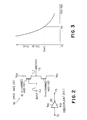
- CMOS gate circuit As shown in FIG. 2, a P-channel MOS-FET 12 and an N-channel MOS-FET 14 are connected in their gates and drains respectively to each other, power source voltages V DD and V SS are respectively applied in sources, signals are applied at the gates via an input terminal 13, and inverted signals of the input signals are taken out from an output terminal 15 via drains.
- a delay time occurs between input and output in such a CMOS gate circuit 10. As shown in FIG. 3, the delay time depends on the power source voltage V DD - V SS , and the smaller the power source voltage V DD - V SS is, the larger become the delay time and the rate of change. This is because the conductance of elements varies depending on the value of the power source voltage V DD - V SS .
- the delay time therefore can be controlled at a desired value by selecting a suitable power source voltage, utilizing the above characteristics.
- the signal delay circuit with CMOS gate circuit 10 of this type is applicable , for instance, in techniques for delaying pulse-frequency modulation (PFM) signals including analog data in time base (e.g. absorption of jitter or of fluctuation in time base among reproduced video signals in a video disc playback device).
- PFM pulse-frequency modulation
- reproduced video signals including jitters are applied at a CMOS gate circuit, color bursts are extracted from the video signals outputted from the CMOS gate circuit, the extracted signals are compared in phase with a crystal oscillated clock of 3.58 MHz corresponding to the subcarrier of the color bursts to derive a phase error, and the power source voltage V DD - V SS in the CMOS gate circuit is controlled in accordance with the phase error to thereby output video signals from the CMOS gate circuit from which jitters have already been absorbed.
- CMOS gate circuits 10 When a long delay time is required, CMOS gate circuits 10 should be connected in multiple-stage as shown in FIG. 4. When they are integrated at ICs, power source lines 16, 17 should be wired in a long distance. By integration, howeber, as the width of the power lines 16, 17 decreases and the impedance of the lines accordingly increases, power source voltage changes unexpectedly to cause the delay time control unstable.
- This invention attenpts to solve such a problem by folding a continuous patter of CMOS gate circuits in multiple-stage connection as is described in more detail hereinafter.
- CMOS integrated circuit for signal delay which is capable of reducing the length of power lines to prevent an increase in impedance therein and of preventing output waveform distortion by arranging CMOS gate circuits in a folded pattern without causing the inconveniences from such folded pattern of CMOS gate circuits.
- the CMOS integrated circuit for signal delay achieving the object of the invention is characterized in that it comprises CMOS gate circuits connected in multiple-stages which deliver out an input binary signal after delaying it by a predetermined delay time, the CMOS gate circuits being arranged in a folded pattern on an integrated circuit substrate and each row of the folded pattern including a part of the CMOS fate circuits in stages of an odd number.
- this invention enables power source line (V DD , V SS ) to be wired in a manner to oppose each other alternately as in the forms of combs.
- this invention can minimize disadvantageous influence of the increased impedance in power source lines.
- each row By forming each row with CMOS gate circuits of an odd number, the factors to cause fluctuation in delay time at folding positions can be effectively offset to thereby make delay times at the rise and fall portions (T R , T F ) in the whole circuit uniform and thus prevent occurrence of output waveform distortion.
- each of the CMOS gate circuits consists of an N channel element and a P channel element connected in series to each other and gate pattern of the respective channels have their width and length adjusted in such a manner that values of operating currents in these elements become equal to each other when the same external voltage has been applied to these elements.
- the ratio of width to length of the gate pattern of the N channel element is smaller than that of the gate pattern of the P channel element.
- CMOS gate circuit having a large current supply capacity at the last stage of each row.
- each row is devided into blocks of an odd number having stages of an odd number and a CMOS gate circuit having a large current supply capacity is arranged at the last stage of each block.
- the period of input signals is an integer multiple of delay times at each stage, operating timing of each CMOS gate element becomes staggered even for periodic input to thereby prevent concentration of operating current.
- power source voltages V DD and V SS nor unexpected changes in delay times to thereby enable transmission to be carried out without waveform distortion between input and output.
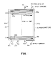
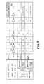
- FIG. 1 shows an embodiment of a chip pattern of CMOS integrated circuits for signal delay according to this invention.
- each short line 20 represents an individual CMOS gate circuit.
- a row 22 comprises an odd number of CMOS gate circuits 20 connected in series. The pattern is folded at an end to form the next row and thereby forms a continuous pattern of a signal delay circuit as a whole.
- a binary signal is applied at an input terminal 24, and a delay output is taken out from an output terminal 26.
- a power source line 28 comprises branch lines 28b in a comb form which are lead out from a bus 28a to supply power source voltage V SS to each row 22 via terminals 28c.
- a power source line 30 comprises branch lines 30b in a comb form which are led out from a bus 30a to oppose the branch lines 28b in a staggered fashion and supplies each row 22 with power source voltage V DD via terminals 30c. The delay time is controlled by such power source voltages V DD and V SS .
- CMOS gate circuits 20 in each row 22 are odd numbered, and in this particular embodiment the number is 231, while the number of rows is 44.
- CMOS gate circuit 20 of the present embodiment There are two types of chip patterns in the CMOS gate circuit 20 of the present embodiment; i.e. type A for small current and type B for large current.
- Type B is arranged at the last stage of each row and of the block obtained by dividing each row by odd number of stages while type A is arranged at positions other than above.
- two CMOS gate circuits are united as a set. Two circuits may be grouped; A-A (a set of two As), A-B (a set of type A followed by type B) , and B-A ( a set of type B followed by type A).
- A-A a set of two As
- A-B a set of type A followed by type B
- B-A a set of type B followed by type A
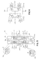
- FIG. 5 shows an example of chip pattern of types A-B.
- FIG. 6 shows the electric circuit thereof.
- This CMOS gate circuit comprises type A and B CMOS gate circuits 20 -1, and 20 - 2 in serial connection.
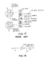
- the chip pattern in a conventional CMOS gate arranges P channel side and N channel side in a symmetrical arrangement as shown in FIG. 17.
- the one shown in FIG. 5 differs between P channel side and N channel side. If they are arranged symmetrically, there arises difference in the characteristics between the rise portion and the fall portion of an output due to difference in characteristics between P channel and N channel with resulting change in duty factor between input and output pulse waveforms when applied in jitter absorption of pulse-frequency modulation signals in video disc reproduction as described above.
- the delay circuit then has difficulty in faithful reproduction of recorded data from a disc.
- charge and discharge currents flow when its output is inverted owing to load capacity C formed in the output side as shown in FIG. 18 and delay characteristic of the CMOS gate circuit 10 is determined by characteristics of the charge and discharge currents.
- I DS K ⁇ 2 ( V GS - V th ) V DS - V DS 2 ⁇ . . . .
- I DS K ( V GS - V th )2 . . . . .
- K is a constant whose value is determined by factors including the type of gate metal, type and thickness of gate insulating material, concentrations of impurities in the substrate silicon, potential difference between the source and the substrate and size of the gate and is expressed by the following equation:
- L and W represent length and width of channels of the MOS-FET, ⁇ ox and t ox dielectric constant and thickness of gate oxide film, and ⁇ mobility of carrier in the channels.
- V th in the above equations can be given by the following equation: ⁇ MS represents difference in work function of metal silicon, Q SS surface level charge density which is + when the substrate is P (N channel MOS-FET) and - when the substrate is N (P channel MOS-FET), and ⁇ F Fermi level of the substrate.
- K' and V th are values which are solely determined during the process of manufacture (though there is difference in the value between the P channel and the N channel) and V GS and V DS are external operating voltages with W/L being their variation factor. If, accordingly, the P channel and the N channel are of the same W/L as in the conventional CMOS gate circuit shown in Fig. 17, I DS of the P channel becomes different from I DS of the N channel under the same voltage condition. That is, charge/discharge times of the capacity differs between the P channel and the N channel. Since K' of the P channel is generally smaller, I DS of the P channel is smaller with a result that charge time (rise time T R )is longer and discharge time (fall time T F ) is shorter.
- distortion in waveform i.e., omission of information in time base
- the width and length of gate patterns of N and P channel elements are adjusted, as shown in FIG. 5, in such a manner that the value of operating current of each channel element becomes equal when the same external voltage condition is given to each channel element.
- the rise time T R and the fall time T F become equal to each other and the waveform distortion between the input and output signals can thereby be prevented.
- a CMOS gate circuit 20 - 1 comprises a P channel MOS-FET 1 and an N channel MOS-FET 2.
- An input signal via a line 24 is applied to gates G pl , G nl through a terminal 22 at the first stage 20 - 1.
- the power source V DD is applied at a source S pl via an electrode 26.
- the power source V SS is applied at a source S nl via an electrode 28.
- the output signals from drains D pl , D nl are applied at gates G p2 and G n2 at the second stage 20 - 2 via a line 31 through a terminal 30.
- the power source V DD is applied at a source S p2 via the electrode 26.
- the power source V SS is applied at a source S n2 via the electrode 28.
- the output signals from drains D p2 and D n2 are taken out via a terminal 32.
- the CMOS gate circuit 20 - 1 of type A is adjusted to have suitable width (W)/Length (L) of the gates G pl and G nl in a manner to have the same I DS when the same power source voltage V DD , V SS is applied on the P channel MOS-FET 1 and N channel MOS-FET 2 depending on the constant K' which is determinable by the structure of each channel element and characterisitics of their materials and the value of threshold voltage V th .
- K' which is determinable by the structure of each channel element and characterisitics of their materials and the value of threshold voltage V th .
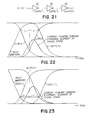
- FIG. 22 In a case where the CMOS gate circuit 20 - 1 of type A is constructed according to these values and three of such CMOS gate circuit 20 - 1 are serially connected as shown in FIG. 21, input and output waveforms thereof are shown in FIGS. 22 and 23.
- FIG. 22 shown rising of the input waveform while FIG. 23 shows falling.
- the CMOS gate circuit 20 - 2 of type B is adjusted to have a suitable width (W)/Length (L) of the gates G p2 and G n2 depending on K' and V th of each channel element in such a manner that the same I DS is obtained when the same power source valtage V DD , V SS is given to the P channel MOS-FET 3 and N channel MOS-FET 4.
- W/L of N channel MOS-FET 3 becomes smaller than W/L of P channel MOS-FET 4.
- the table below shows an example of dimensions of the gates G p2 and G n2 .
- type B has 1.6 times more of the current supply capacity than type A.
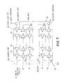
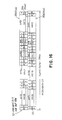
- the electric circuit of the chip pattern shown in FIG. 1 is shown in FIG. 7.
- the chip pattern is formed by folding a continuous pattern comprising CMOS gate circuits 20 in multiple-stage connection to have an odd number of circuits in each row and signals applied at an input terminal 24 are delayed at each stage and taken out from an output terminal 26.
- CMOS gate circuits 20 can be effective severelyly arranged on a limited space of a chip substrate.
- the power source line 28 is led out by comb-like branch lines 28b from a bus 28a to supply power source voltage V SS to each CMOS gate circuit 20.
- the power source line 30 is led out from a bus 30a by comb-like branch lines 30b to supply power source V DD to each CMOS gate circuit 20.
- Each CMOS gate circuit 20 per se is adjusted in the width (W)/length (L) of gate in a manner to make current characteristics of P and N channels identical. However, even after such an adjustment, a slight difference may possibly be caused between t r (delay time entailed by inversion in rising) and t f (delay time entailed by inversion in falling) of each CMOS gate circuit 20.
- T r 100t f + 100t r
- T f 100t r + 100t f
- the load capacity at the folding position becomes (1 + K) compared to the standard load (1) at other portions or an increase of load capacity by K at the final stage ( the 200th stage) arises due to to the patterned wiring at the portion 36.
- ⁇ T
- K
- If there are n rows, the difference as a whole chip will be n ⁇ T n ⁇ K
- one row 22 comprises 201 stages as shown in FIG. 9.
- T r2 100t r + 100t f + t r (l + K)
- T f2 100t f + 100t r + t f (l + K)
- ⁇ T1 + ⁇ T2 0
- the delay time distortion in output waveforms is completely offset by setting the number of stages of one row 22 at 231 and the number of rows for the chip at 44.
- the difference in delay time between rising and falling is offset by setting the number of stages for one row 22 at an odd number.
- the difference will be more completely offset in a chip as a whole irrespective of the number of rows if the increase of K due to the increase in load capacity at the folding portion 36 should be offset for each row.
- the current supply capacity of the CMOS gate circuit 20 at the last stage of each row should be increased in correspondence to the increase of K due to the increase in load capacity. More particularly, driving capacity of a CMOS gate circuit is increased to (l + K) times magnitude of type A by using type B 20 - 2 shown in FIG. 5 so as to correspond to the increase of K value.
- Such a structure has another merit that the upper limit of frequencies of delayable signals will not be lowered. More specifically, when the current supply capacity at the folding portion 36 of a CMOS gate circuit is the same as other portions, the load capacity increases in response to the increase of K value and it takes more time for charging/discharging the capacity, thereby increasing the delay time more than those at the other portion. In other words,it takes more time for signal inversion. It therefore cannot quite follow the input changes at high frequencies. Unless the folding portion 36 is strengthened, it will become a bottle neck lowering the upper limit of operable frequencies and in the worst case, causing signals to disappear midway of stages.
- CMOS gate circuits with stages of the integer in between operate at the same timing.
- CMOS gate circuits When CMOS gate circuits operate, operating current as shown in FIG. 11 flows in the power source lines. In this case, the current in the amount equivalent to the number of circuits which operate at the same timing flows in the power source lines.
- impedance of a certain level always exists in the power source lines, if the concentration of current reaches a certain degree, unexpected power source voltage drop will occur at each period to give adverse influence to the delay time control operation.
- Pulse frequency modulated signals for video discs are standardized to vary the period thereof between frequencies 7.6 - 9.3 MHz. Regardless of the value of the delay time, so long as it is the same for a group of circuits, such phenomenon as the concentration of operating currents always and unavoidably occurs at a certain frequency. The phenomenon occurs because the CMOS gate circuits a , b , c . . . rise and fall at the same timing as shown in FIG.12a. The operating timing should be staggered to solve the problem. In other words, delay time among the circuits a , b and c should be set at different values as shown in FIG. 12b.
- FIG. 13 shows the changes of operating currents against the period of input signals in two rows which are related to one branch line of the current line 28 when one row comprises 231 stages of type A 20 - 1 and the delay time for one stage is set at 2.9 ns.
- the changes are shown in the graph for the scope of 7.6 - 9.3 MHz which is mentioned above, and the direct current component is removed to indicate only the alternating component in the operating current.
- the sloped line in the upper portion of the graph represents the maximum number of stages of current concentration which theoretically could occur in two rows. This maximum number of stages corresponds to all the values of currents in the two rows when the operating current value for one stage is set as a reference 1.
- the operating current concentration occurs at multiples of 2.9 ns by integers such as 110.2 ns (equivalent to the delay time for 38 stages), 113.1 ns (for 39 stages), 116.0 ns (40 stages), 118.9 ns (41 stages), 121.8 ns (42 stages), 124.7 ns (43 stages), 127.6 ns (44 stages), and 130.5 ns (45 stages).
- operating timing should be suitably varied within a row 22 be dividing, as shown in FIG. 14, a row into blocks in an odd number each comprising CMOS gate circuits 20 in an odd number and arranging type B 20 - 2 of FIG. 5 with a larger current supply capacity at the last gate of each block to thereby make the structure non-periodical.
- the operating current can be dispersed for all the range of frequencies.
- the range of input signal frequencies should be considered for two periods and therefore, the numbers should be chosen in a manner to stagger timing.
- the delay time for oneestage is set st 2.9 ns , coincidence in timings for two periods will appear in the numbers of stages shown in the Table.
- the number of stages in a block should be determined by removing the values in proximity of the stages shown in the table and constructing one row with, for instance, 73, 59, 15, 19 and 65 in combination.
- FIG. 15 shows changes in the operating current for two rows in relation with the periods of input signals. This indicates that operating currents are distributed across all the range of frequencies.
- each branch line 28b or 30b may be considered taking each branch line 28b or 30b as a unit. Therefore, it will suffice if above processing should be effected in the unit of two rows on which one branch line could influence.
- FIG. 16 shows an example of chip pattern for two rows which is structured by giving due consideration to the above points.
- the characters [AB] denote a combination of A-type 20 -1 and B-type 20 - 2 as shown in FIG. 5, [BA] a combination of A and B types in the reverse order, [AA] a combination of two As, and [B] a pattern with a single B-type 20 - 2.
Landscapes
- Physics & Mathematics (AREA)
- Nonlinear Science (AREA)
- Pulse Circuits (AREA)
Applications Claiming Priority (4)
| Application Number | Priority Date | Filing Date | Title |
|---|---|---|---|
| JP60221787A JPS6282716A (ja) | 1985-10-07 | 1985-10-07 | 信号遅延用cmos集積回路 |
| JP221786/85 | 1985-10-07 | ||
| JP60221786A JPS6282715A (ja) | 1985-10-07 | 1985-10-07 | Cmosゲ−ト回路 |
| JP221787/85 | 1985-10-07 |
Publications (3)
| Publication Number | Publication Date |
|---|---|
| EP0219291A2 true EP0219291A2 (de) | 1987-04-22 |
| EP0219291A3 EP0219291A3 (en) | 1989-03-01 |
| EP0219291B1 EP0219291B1 (de) | 1992-03-11 |
Family
ID=26524503
Family Applications (1)
| Application Number | Title | Priority Date | Filing Date |
|---|---|---|---|
| EP86307690A Expired EP0219291B1 (de) | 1985-10-07 | 1986-10-06 | CMOS-integrierte Verzögerungsschaltung |
Country Status (3)
| Country | Link |
|---|---|
| US (1) | US4742254A (de) |
| EP (1) | EP0219291B1 (de) |
| DE (1) | DE3684222D1 (de) |
Cited By (2)
| Publication number | Priority date | Publication date | Assignee | Title |
|---|---|---|---|---|
| EP0334983A1 (de) * | 1988-03-31 | 1989-10-04 | Deutsche ITT Industries GmbH | Integrierte CMOS/NMOS-Schaltung |
| EP0704970A1 (de) * | 1994-09-29 | 1996-04-03 | Valeo Electronique | Mono-Flop mit einer geringen Übergangszeitenfehlanpassung und diesen enthaltende elektronische Schaltung |
Families Citing this family (9)
| Publication number | Priority date | Publication date | Assignee | Title |
|---|---|---|---|---|
| JPH083773B2 (ja) * | 1987-02-23 | 1996-01-17 | 株式会社日立製作所 | 大規模半導体論理回路 |
| US5173617A (en) * | 1988-06-27 | 1992-12-22 | Motorola, Inc. | Digital phase lock clock generator without local oscillator |
| EP0357410B1 (de) * | 1988-09-01 | 1993-11-03 | Fujitsu Limited | Integrierter Halbleiterschaltkreis |
| US5192886A (en) * | 1990-03-15 | 1993-03-09 | Hewlett-Packard Company | Sub-nanosecond calibrated delay line structure |
| JP3605122B2 (ja) * | 1991-12-13 | 2004-12-22 | テキサス インスツルメンツ インコーポレイテツド | 補償回路と遅延を補償する方法 |
| TW253083B (de) * | 1993-10-05 | 1995-08-01 | Advanced Micro Devices Inc | |
| JP2000059185A (ja) * | 1998-08-14 | 2000-02-25 | Nec Corp | 同期遅延回路 |
| US6288587B1 (en) * | 1999-04-07 | 2001-09-11 | National Science Council Of Republic Of China | CMOS pulse shrinking delay element with deep subnanosecond resolution |
| TWI283143B (en) * | 2002-12-03 | 2007-06-21 | Au Optronics Corp | Structure and method for reducing the resistance of power line, suitable for use in a LED displayer |
Family Cites Families (8)
| Publication number | Priority date | Publication date | Assignee | Title |
|---|---|---|---|---|
| US3378783A (en) * | 1965-12-13 | 1968-04-16 | Rca Corp | Optimized digital amplifier utilizing insulated-gate field-effect transistors |
| US3921101A (en) * | 1973-10-05 | 1975-11-18 | Electronic Arrays | Mosfet clock |
| US3931588A (en) * | 1974-09-10 | 1976-01-06 | Rca Corporation | Voltage controlled oscillator utilizing field effect transistors |
| US4069429A (en) * | 1976-09-13 | 1978-01-17 | Harris Corporation | IGFET clock generator |
| US4344002A (en) * | 1978-02-22 | 1982-08-10 | Supertex, Inc. | Detection circuit and structure therefor |
| CA1165387A (en) * | 1981-10-02 | 1984-04-10 | Larry J. Conway | Sampling frequency converter |
| CA1165890A (en) * | 1982-03-18 | 1984-04-17 | Trevor W. Tucker | Sampling spectrum analyzer |
| EP0390226A1 (de) * | 1984-07-31 | 1990-10-03 | Yamaha Corporation | Absorptionsschaltung des Zitterns |
-
1986
- 1986-10-01 US US06/914,377 patent/US4742254A/en not_active Expired - Lifetime
- 1986-10-06 DE DE8686307690T patent/DE3684222D1/de not_active Expired - Lifetime
- 1986-10-06 EP EP86307690A patent/EP0219291B1/de not_active Expired
Cited By (4)
| Publication number | Priority date | Publication date | Assignee | Title |
|---|---|---|---|---|
| EP0334983A1 (de) * | 1988-03-31 | 1989-10-04 | Deutsche ITT Industries GmbH | Integrierte CMOS/NMOS-Schaltung |
| US4922140A (en) * | 1988-03-31 | 1990-05-01 | Deutsche Itt Industries Gmbh | CMOS/NMOS integrated circuit with supply voltage delay variation compensation |
| EP0704970A1 (de) * | 1994-09-29 | 1996-04-03 | Valeo Electronique | Mono-Flop mit einer geringen Übergangszeitenfehlanpassung und diesen enthaltende elektronische Schaltung |
| FR2725325A1 (fr) * | 1994-09-29 | 1996-04-05 | Valeo Electronique | Circuit monostable a faibles dispersions du temps de basculement et circuit electronique l'incorporant |
Also Published As
| Publication number | Publication date |
|---|---|
| DE3684222D1 (de) | 1992-04-16 |
| US4742254A (en) | 1988-05-03 |
| EP0219291A3 (en) | 1989-03-01 |
| EP0219291B1 (de) | 1992-03-11 |
Similar Documents
| Publication | Publication Date | Title |
|---|---|---|
| EP0219291A2 (de) | CMOS-integrierte Verzögerungsschaltung | |
| US5694065A (en) | Switching control circuitry for low noise CMOS inverter | |
| KR0153245B1 (ko) | 프로그래머블 지연회로 | |
| EP0656688B1 (de) | Taktsignalgenerator für eine Vielzahl nicht überlappender Taktsignale | |
| KR100568075B1 (ko) | 반도체집적회로장치 | |
| US6172545B1 (en) | Delay circuit on a semiconductor device | |
| JP2008277842A (ja) | 分散されたゲートドライバを備えた電源集積回路 | |
| US5173618A (en) | Clock generator for providing a pair of nonoverlapping clock signals with adjustable skew | |
| JPH0454724A (ja) | 論理回路 | |
| US5391904A (en) | Semiconductor delay circuit device | |
| US5389831A (en) | Clock generator for providing a pair of nonoverlapping clock signals with adjustable skew | |
| US5489860A (en) | Semiconductor circuit having improved layout pattern | |
| US4521898A (en) | Ripple counter circuit having reduced propagation delay | |
| JPH0537300A (ja) | スイツチトキヤパシタ回路 | |
| EP0676863B1 (de) | Spannungsgesteuerte Oszillatorschaltung | |
| JP2739958B2 (ja) | スタンダードセル | |
| JPH0344426B2 (de) | ||
| KR19980051304A (ko) | 펄스폭 제어가 가능한 주파스 체배기 | |
| US5619146A (en) | Switching speed fluctuation detecting apparatus for logic circuit arrangement | |
| US6268757B1 (en) | Semiconductor device having capacitor that reduce fluctuation of power supply | |
| JPS6327897B2 (de) | ||
| KR930000959B1 (ko) | 데이터 출력회로 | |
| Yanagisawa et al. | Gigabit rate Gunn-effect shift register | |
| US4439753A (en) | Thick film printed circuit | |
| JP2548495Y2 (ja) | 可変遅延装置 |
Legal Events
| Date | Code | Title | Description |
|---|---|---|---|
| PUAI | Public reference made under article 153(3) epc to a published international application that has entered the european phase |
Free format text: ORIGINAL CODE: 0009012 |
|
| AK | Designated contracting states |
Kind code of ref document: A2 Designated state(s): DE GB |
|
| 17P | Request for examination filed |
Effective date: 19870827 |
|
| RAP1 | Party data changed (applicant data changed or rights of an application transferred) |
Owner name: YAMAHA CORPORATION |
|
| PUAL | Search report despatched |
Free format text: ORIGINAL CODE: 0009013 |
|
| AK | Designated contracting states |
Kind code of ref document: A3 Designated state(s): DE GB |
|
| 17Q | First examination report despatched |
Effective date: 19900713 |
|
| GRAA | (expected) grant |
Free format text: ORIGINAL CODE: 0009210 |
|
| AK | Designated contracting states |
Kind code of ref document: B1 Designated state(s): DE GB |
|
| REF | Corresponds to: |
Ref document number: 3684222 Country of ref document: DE Date of ref document: 19920416 |
|
| PLBE | No opposition filed within time limit |
Free format text: ORIGINAL CODE: 0009261 |
|
| STAA | Information on the status of an ep patent application or granted ep patent |
Free format text: STATUS: NO OPPOSITION FILED WITHIN TIME LIMIT |
|
| 26N | No opposition filed | ||
| REG | Reference to a national code |
Ref country code: GB Ref legal event code: IF02 |
|
| PGFP | Annual fee paid to national office [announced via postgrant information from national office to epo] |
Ref country code: DE Payment date: 20050929 Year of fee payment: 20 |
|
| PGFP | Annual fee paid to national office [announced via postgrant information from national office to epo] |
Ref country code: GB Payment date: 20051005 Year of fee payment: 20 |
|
| PG25 | Lapsed in a contracting state [announced via postgrant information from national office to epo] |
Ref country code: GB Free format text: LAPSE BECAUSE OF EXPIRATION OF PROTECTION Effective date: 20061005 |
|
| REG | Reference to a national code |
Ref country code: GB Ref legal event code: PE20 |