EP0214733A2 - Tête d'impression thermique à jet d'encre de haute résolution - Google Patents
Tête d'impression thermique à jet d'encre de haute résolution Download PDFInfo
- Publication number
- EP0214733A2 EP0214733A2 EP86305645A EP86305645A EP0214733A2 EP 0214733 A2 EP0214733 A2 EP 0214733A2 EP 86305645 A EP86305645 A EP 86305645A EP 86305645 A EP86305645 A EP 86305645A EP 0214733 A2 EP0214733 A2 EP 0214733A2
- Authority
- EP
- European Patent Office
- Prior art keywords
- printhead
- ink
- grooves
- electrodes
- parts
- Prior art date
- Legal status (The legal status is an assumption and is not a legal conclusion. Google has not performed a legal analysis and makes no representation as to the accuracy of the status listed.)
- Granted
Links
- 238000010438 heat treatment Methods 0.000 claims abstract description 81
- 238000000034 method Methods 0.000 claims abstract description 16
- 238000005530 etching Methods 0.000 claims description 22
- 239000003351 stiffener Substances 0.000 claims description 16
- XUIMIQQOPSSXEZ-UHFFFAOYSA-N Silicon Chemical compound [Si] XUIMIQQOPSSXEZ-UHFFFAOYSA-N 0.000 claims description 14
- 239000000463 material Substances 0.000 claims description 14
- 229910052710 silicon Inorganic materials 0.000 claims description 14
- 239000010703 silicon Substances 0.000 claims description 14
- 238000002161 passivation Methods 0.000 claims description 12
- 239000000758 substrate Substances 0.000 claims description 12
- 238000003491 array Methods 0.000 claims description 7
- 230000004044 response Effects 0.000 claims description 5
- 239000011248 coating agent Substances 0.000 claims description 4
- 238000000576 coating method Methods 0.000 claims description 4
- 238000004891 communication Methods 0.000 claims description 4
- 230000015572 biosynthetic process Effects 0.000 claims description 3
- 238000000151 deposition Methods 0.000 claims description 3
- 230000013011 mating Effects 0.000 claims description 3
- 238000000059 patterning Methods 0.000 claims description 2
- 238000012546 transfer Methods 0.000 claims description 2
- 230000000149 penetrating effect Effects 0.000 claims 2
- 238000004140 cleaning Methods 0.000 claims 1
- 239000004020 conductor Substances 0.000 claims 1
- 238000009413 insulation Methods 0.000 claims 1
- 239000000976 ink Substances 0.000 description 73
- 239000010410 layer Substances 0.000 description 28
- 235000012431 wafers Nutrition 0.000 description 27
- 238000007639 printing Methods 0.000 description 10
- VYPSYNLAJGMNEJ-UHFFFAOYSA-N Silicium dioxide Chemical compound O=[Si]=O VYPSYNLAJGMNEJ-UHFFFAOYSA-N 0.000 description 8
- 238000004519 manufacturing process Methods 0.000 description 7
- 229910021420 polycrystalline silicon Inorganic materials 0.000 description 7
- 229910052581 Si3N4 Inorganic materials 0.000 description 6
- 229920005591 polysilicon Polymers 0.000 description 6
- 239000011241 protective layer Substances 0.000 description 6
- HQVNEWCFYHHQES-UHFFFAOYSA-N silicon nitride Chemical compound N12[Si]34N5[Si]62N3[Si]51N64 HQVNEWCFYHHQES-UHFFFAOYSA-N 0.000 description 5
- KWYUFKZDYYNOTN-UHFFFAOYSA-M Potassium hydroxide Chemical compound [OH-].[K+] KWYUFKZDYYNOTN-UHFFFAOYSA-M 0.000 description 4
- 229910052782 aluminium Inorganic materials 0.000 description 4
- XAGFODPZIPBFFR-UHFFFAOYSA-N aluminium Chemical compound [Al] XAGFODPZIPBFFR-UHFFFAOYSA-N 0.000 description 4
- 238000005229 chemical vapour deposition Methods 0.000 description 4
- 229910052681 coesite Inorganic materials 0.000 description 4
- 229910052906 cristobalite Inorganic materials 0.000 description 4
- 230000008569 process Effects 0.000 description 4
- 239000000377 silicon dioxide Substances 0.000 description 4
- 235000012239 silicon dioxide Nutrition 0.000 description 4
- 229910052682 stishovite Inorganic materials 0.000 description 4
- 229910052905 tridymite Inorganic materials 0.000 description 4
- 239000000853 adhesive Substances 0.000 description 3
- 230000001070 adhesive effect Effects 0.000 description 3
- 230000008901 benefit Effects 0.000 description 3
- 238000007641 inkjet printing Methods 0.000 description 3
- 230000005499 meniscus Effects 0.000 description 3
- 150000004767 nitrides Chemical class 0.000 description 3
- 238000007789 sealing Methods 0.000 description 3
- 239000004593 Epoxy Substances 0.000 description 2
- 230000009471 action Effects 0.000 description 2
- 239000003822 epoxy resin Substances 0.000 description 2
- 239000007788 liquid Substances 0.000 description 2
- 238000012986 modification Methods 0.000 description 2
- 230000004048 modification Effects 0.000 description 2
- 229920003223 poly(pyromellitimide-1,4-diphenyl ether) Polymers 0.000 description 2
- 229920000647 polyepoxide Polymers 0.000 description 2
- 238000012545 processing Methods 0.000 description 2
- 238000004544 sputter deposition Methods 0.000 description 2
- ZOXJGFHDIHLPTG-UHFFFAOYSA-N Boron Chemical compound [B] ZOXJGFHDIHLPTG-UHFFFAOYSA-N 0.000 description 1
- 229910007948 ZrB2 Inorganic materials 0.000 description 1
- 230000001133 acceleration Effects 0.000 description 1
- 230000000712 assembly Effects 0.000 description 1
- 238000000429 assembly Methods 0.000 description 1
- QVGXLLKOCUKJST-UHFFFAOYSA-N atomic oxygen Chemical compound [O] QVGXLLKOCUKJST-UHFFFAOYSA-N 0.000 description 1
- 238000010923 batch production Methods 0.000 description 1
- 230000000903 blocking effect Effects 0.000 description 1
- 229910052796 boron Inorganic materials 0.000 description 1
- VWZIXVXBCBBRGP-UHFFFAOYSA-N boron;zirconium Chemical compound B#[Zr]#B VWZIXVXBCBBRGP-UHFFFAOYSA-N 0.000 description 1
- 238000010276 construction Methods 0.000 description 1
- 230000008602 contraction Effects 0.000 description 1
- 239000002537 cosmetic Substances 0.000 description 1
- 239000002178 crystalline material Substances 0.000 description 1
- 230000003247 decreasing effect Effects 0.000 description 1
- 230000008021 deposition Effects 0.000 description 1
- 238000001312 dry etching Methods 0.000 description 1
- 238000005516 engineering process Methods 0.000 description 1
- 238000011049 filling Methods 0.000 description 1
- 239000011521 glass Substances 0.000 description 1
- 238000000227 grinding Methods 0.000 description 1
- BHEPBYXIRTUNPN-UHFFFAOYSA-N hydridophosphorus(.) (triplet) Chemical compound [PH] BHEPBYXIRTUNPN-UHFFFAOYSA-N 0.000 description 1
- 230000003993 interaction Effects 0.000 description 1
- 238000002955 isolation Methods 0.000 description 1
- 229910052751 metal Inorganic materials 0.000 description 1
- 239000002184 metal Substances 0.000 description 1
- 238000003801 milling Methods 0.000 description 1
- 229910021421 monocrystalline silicon Inorganic materials 0.000 description 1
- 230000006911 nucleation Effects 0.000 description 1
- 238000010899 nucleation Methods 0.000 description 1
- 229910052760 oxygen Inorganic materials 0.000 description 1
- 239000001301 oxygen Substances 0.000 description 1
- 230000003094 perturbing effect Effects 0.000 description 1
- 239000005360 phosphosilicate glass Substances 0.000 description 1
- 238000000206 photolithography Methods 0.000 description 1
- 238000001020 plasma etching Methods 0.000 description 1
- 230000001681 protective effect Effects 0.000 description 1
- 239000000565 sealant Substances 0.000 description 1
- 239000004065 semiconductor Substances 0.000 description 1
- 238000000926 separation method Methods 0.000 description 1
- 229910052715 tantalum Inorganic materials 0.000 description 1
- GUVRBAGPIYLISA-UHFFFAOYSA-N tantalum atom Chemical compound [Ta] GUVRBAGPIYLISA-UHFFFAOYSA-N 0.000 description 1
- 238000012360 testing method Methods 0.000 description 1
- 229920001187 thermosetting polymer Polymers 0.000 description 1
- 238000001039 wet etching Methods 0.000 description 1
Images


Classifications
-
- B—PERFORMING OPERATIONS; TRANSPORTING
- B41—PRINTING; LINING MACHINES; TYPEWRITERS; STAMPS
- B41J—TYPEWRITERS; SELECTIVE PRINTING MECHANISMS, i.e. MECHANISMS PRINTING OTHERWISE THAN FROM A FORME; CORRECTION OF TYPOGRAPHICAL ERRORS
- B41J2/00—Typewriters or selective printing mechanisms characterised by the printing or marking process for which they are designed
- B41J2/005—Typewriters or selective printing mechanisms characterised by the printing or marking process for which they are designed characterised by bringing liquid or particles selectively into contact with a printing material
- B41J2/01—Ink jet
- B41J2/135—Nozzles
- B41J2/16—Production of nozzles
- B41J2/1621—Manufacturing processes
- B41J2/1631—Manufacturing processes photolithography
-
- B—PERFORMING OPERATIONS; TRANSPORTING
- B41—PRINTING; LINING MACHINES; TYPEWRITERS; STAMPS
- B41J—TYPEWRITERS; SELECTIVE PRINTING MECHANISMS, i.e. MECHANISMS PRINTING OTHERWISE THAN FROM A FORME; CORRECTION OF TYPOGRAPHICAL ERRORS
- B41J2/00—Typewriters or selective printing mechanisms characterised by the printing or marking process for which they are designed
- B41J2/005—Typewriters or selective printing mechanisms characterised by the printing or marking process for which they are designed characterised by bringing liquid or particles selectively into contact with a printing material
- B41J2/01—Ink jet
- B41J2/135—Nozzles
- B41J2/14—Structure thereof only for on-demand ink jet heads
- B41J2/14016—Structure of bubble jet print heads
- B41J2/14032—Structure of the pressure chamber
- B41J2/1404—Geometrical characteristics
-
- B—PERFORMING OPERATIONS; TRANSPORTING
- B41—PRINTING; LINING MACHINES; TYPEWRITERS; STAMPS
- B41J—TYPEWRITERS; SELECTIVE PRINTING MECHANISMS, i.e. MECHANISMS PRINTING OTHERWISE THAN FROM A FORME; CORRECTION OF TYPOGRAPHICAL ERRORS
- B41J2/00—Typewriters or selective printing mechanisms characterised by the printing or marking process for which they are designed
- B41J2/005—Typewriters or selective printing mechanisms characterised by the printing or marking process for which they are designed characterised by bringing liquid or particles selectively into contact with a printing material
- B41J2/01—Ink jet
- B41J2/135—Nozzles
- B41J2/145—Arrangement thereof
- B41J2/15—Arrangement thereof for serial printing
-
- B—PERFORMING OPERATIONS; TRANSPORTING
- B41—PRINTING; LINING MACHINES; TYPEWRITERS; STAMPS
- B41J—TYPEWRITERS; SELECTIVE PRINTING MECHANISMS, i.e. MECHANISMS PRINTING OTHERWISE THAN FROM A FORME; CORRECTION OF TYPOGRAPHICAL ERRORS
- B41J2/00—Typewriters or selective printing mechanisms characterised by the printing or marking process for which they are designed
- B41J2/005—Typewriters or selective printing mechanisms characterised by the printing or marking process for which they are designed characterised by bringing liquid or particles selectively into contact with a printing material
- B41J2/01—Ink jet
- B41J2/135—Nozzles
- B41J2/16—Production of nozzles
- B41J2/1601—Production of bubble jet print heads
- B41J2/1604—Production of bubble jet print heads of the edge shooter type
-
- B—PERFORMING OPERATIONS; TRANSPORTING
- B41—PRINTING; LINING MACHINES; TYPEWRITERS; STAMPS
- B41J—TYPEWRITERS; SELECTIVE PRINTING MECHANISMS, i.e. MECHANISMS PRINTING OTHERWISE THAN FROM A FORME; CORRECTION OF TYPOGRAPHICAL ERRORS
- B41J2/00—Typewriters or selective printing mechanisms characterised by the printing or marking process for which they are designed
- B41J2/005—Typewriters or selective printing mechanisms characterised by the printing or marking process for which they are designed characterised by bringing liquid or particles selectively into contact with a printing material
- B41J2/01—Ink jet
- B41J2/135—Nozzles
- B41J2/16—Production of nozzles
- B41J2/1621—Manufacturing processes
- B41J2/1623—Manufacturing processes bonding and adhesion
-
- B—PERFORMING OPERATIONS; TRANSPORTING
- B41—PRINTING; LINING MACHINES; TYPEWRITERS; STAMPS
- B41J—TYPEWRITERS; SELECTIVE PRINTING MECHANISMS, i.e. MECHANISMS PRINTING OTHERWISE THAN FROM A FORME; CORRECTION OF TYPOGRAPHICAL ERRORS
- B41J2/00—Typewriters or selective printing mechanisms characterised by the printing or marking process for which they are designed
- B41J2/005—Typewriters or selective printing mechanisms characterised by the printing or marking process for which they are designed characterised by bringing liquid or particles selectively into contact with a printing material
- B41J2/01—Ink jet
- B41J2/135—Nozzles
- B41J2/16—Production of nozzles
- B41J2/1621—Manufacturing processes
- B41J2/1626—Manufacturing processes etching
- B41J2/1628—Manufacturing processes etching dry etching
-
- B—PERFORMING OPERATIONS; TRANSPORTING
- B41—PRINTING; LINING MACHINES; TYPEWRITERS; STAMPS
- B41J—TYPEWRITERS; SELECTIVE PRINTING MECHANISMS, i.e. MECHANISMS PRINTING OTHERWISE THAN FROM A FORME; CORRECTION OF TYPOGRAPHICAL ERRORS
- B41J2/00—Typewriters or selective printing mechanisms characterised by the printing or marking process for which they are designed
- B41J2/005—Typewriters or selective printing mechanisms characterised by the printing or marking process for which they are designed characterised by bringing liquid or particles selectively into contact with a printing material
- B41J2/01—Ink jet
- B41J2/135—Nozzles
- B41J2/16—Production of nozzles
- B41J2/1621—Manufacturing processes
- B41J2/1626—Manufacturing processes etching
- B41J2/1629—Manufacturing processes etching wet etching
-
- B—PERFORMING OPERATIONS; TRANSPORTING
- B41—PRINTING; LINING MACHINES; TYPEWRITERS; STAMPS
- B41J—TYPEWRITERS; SELECTIVE PRINTING MECHANISMS, i.e. MECHANISMS PRINTING OTHERWISE THAN FROM A FORME; CORRECTION OF TYPOGRAPHICAL ERRORS
- B41J2/00—Typewriters or selective printing mechanisms characterised by the printing or marking process for which they are designed
- B41J2/005—Typewriters or selective printing mechanisms characterised by the printing or marking process for which they are designed characterised by bringing liquid or particles selectively into contact with a printing material
- B41J2/01—Ink jet
- B41J2/135—Nozzles
- B41J2/16—Production of nozzles
- B41J2/1621—Manufacturing processes
- B41J2/1632—Manufacturing processes machining
-
- B—PERFORMING OPERATIONS; TRANSPORTING
- B41—PRINTING; LINING MACHINES; TYPEWRITERS; STAMPS
- B41J—TYPEWRITERS; SELECTIVE PRINTING MECHANISMS, i.e. MECHANISMS PRINTING OTHERWISE THAN FROM A FORME; CORRECTION OF TYPOGRAPHICAL ERRORS
- B41J2/00—Typewriters or selective printing mechanisms characterised by the printing or marking process for which they are designed
- B41J2/005—Typewriters or selective printing mechanisms characterised by the printing or marking process for which they are designed characterised by bringing liquid or particles selectively into contact with a printing material
- B41J2/01—Ink jet
- B41J2/135—Nozzles
- B41J2/16—Production of nozzles
- B41J2/1621—Manufacturing processes
- B41J2/164—Manufacturing processes thin film formation
- B41J2/1642—Manufacturing processes thin film formation thin film formation by CVD [chemical vapor deposition]
-
- B—PERFORMING OPERATIONS; TRANSPORTING
- B41—PRINTING; LINING MACHINES; TYPEWRITERS; STAMPS
- B41J—TYPEWRITERS; SELECTIVE PRINTING MECHANISMS, i.e. MECHANISMS PRINTING OTHERWISE THAN FROM A FORME; CORRECTION OF TYPOGRAPHICAL ERRORS
- B41J2/00—Typewriters or selective printing mechanisms characterised by the printing or marking process for which they are designed
- B41J2/005—Typewriters or selective printing mechanisms characterised by the printing or marking process for which they are designed characterised by bringing liquid or particles selectively into contact with a printing material
- B41J2/01—Ink jet
- B41J2/135—Nozzles
- B41J2/16—Production of nozzles
- B41J2/1621—Manufacturing processes
- B41J2/164—Manufacturing processes thin film formation
- B41J2/1646—Manufacturing processes thin film formation thin film formation by sputtering
Definitions
- This invention relates to an ink jet printhead for a drop-on-demand thermal ink jet printer.
- the printer is of the kind comprising a plurality of parallel channels each having associated therewith a heating element.
- This kind of ink jet printer discharges droplets through an orifice on an ink jet printhead, the droplets being propelled by bubble generation at an electrically driven heating element in the printhead.
- the printhead comprises one or more ink filled channels, such as disclosed in U.S. 4,463,359 to Ayata et al, communicating with a relatively small ink supply chamber at one end and having an orifice at the opposite end, sometimes referred to as a nozzle.
- a thermal energy generator or heating element usually a resistor, is located in the channels near the nozzle a predetermined distance therefrom.
- the resistors are individually addressed with a current pulse to momentarily vaporize the ink and form a bubble which expels an ink droplet. As the bubble grows, the ink bulges from the nozzle and is contained by the surface tension of the ink as a meniscus.
- the ink still in the channel between the nozzle and bubble starts to move towards the collapsing bubble, causing a volumetric contraction of the ink at the nozzle and resulting in the separation of the bulging ink as a droplet.
- the acceleration of the ink out of the nozzle while the bubble is growing provides the momentum and velocity of the droplet in a substantially straight line direction towards a recording medium, such as paper.
- a thermal ink jet printer having one or more ink-filled channels which are replenished by capillary action.
- a meniscus is formed at each nozzle to prevent ink from weeping therefrom.
- a resistor or heater is located in each channel at a predetermined distance from the nozzles.
- Current pulses representative of data signals are applied to the resistors to momentarily vaporize the ink in contact therewith and form a bubble for each current pulse.
- Ink droplets are expelled from each nozzle by the growth of the bubbles which causes a quantity of ink to bulge from the nozzle and break off into a droplet at the beginning of the bubble collapse.
- the current pulses are shaped to prevent the meniscus from breaking up and receding too far into the channels, after each droplet is expelled.
- Various embodiments of linear arrays of thermal ink jet devices are shown such as those having staggered linear arrays attached to the top and bottom of a heat sinking substrate and those having different colored inks for multicolored printing.
- a resistor is located in the center of a relatively short channel having nozzles at both ends thereof.
- Another passageway is connected to the open-ended channel and is perpendicular thereto to form a T-shaped structure. Ink is replenished to the open-ended channel from the passageway by capillary action.
- two different recording mediums may be printed simultaneously.
- IBM Technical Disclosure Bulletin, Vol. 21 No. 6, pages 2585-6, dated November 1978 discloses differential etching of mutually perpendicular grooves in opposite surfaces of a (100) oriented silicon wafer. An array of nozzles is formed when the depth of the grooves is equal to one-half of the thickness of the wafer.
- U.S. 4,438,191 to Cloutier et al discloses a method of making a monolithic bubble-driven ink jet printhead which eliminates the need for using adhesives to construct multiple parts assemblies.
- the method provides a layered structure which can be manufactured by standard integrated circuit and printed circuit processing techniques. Basically, the substrate with the bubble generating resistors and individually addressing electrodes have the ink chambers and nozzles formed thereon by standard semiconductor processing.
- U.S. 4,335,389 to Y. Shirato et at discloses a liquid droplet ejecting recording head characterized in that the part of the electrothermal transducer contacting the liquid is made of a material which passes a particular weight decreasing test to assure that it will not wear excessively in the operating environment of growing and collapsing bubbles.
- U.S. 4,377,814 to J. R. Debesis discloses corrugated members between adjacent droplet ejecting housings to isolate one from another to prevent cross-talk or the energization of a nozzle in one of the housings other than the selected one.
- U.S. 4,417,251 to H. Sugitani discloses a method of manufacturing an ink jet head where the channels which constitute the ink flow path from the reservoir to the nozzles are formed in a layer of photosensitive material placed on a substrate.
- Japanese patent application No. 53-122508 to T. Hamano filed October 6, 1978 and published without examination on April 9, 1980 as Laid- Open No. 55-49274, discloses a fabricating technique for making nozzle plates by producing a mold via anisotropically etching of a single crystalline material to form a plurality of mesas.
- Japanese patent application No. 53-122509 to T. Hamano filed October 6, 1978 and published without examination on April 9, 1980 as Laid- Open No 55-49275, discloses two single crystalline layers which sandwich therebetween an etching protective layer formed by boron doping of one of the confronting surfaces of the crystalline layers.
- An identically patterned protective layer is formed on each of the outer surfaces of the crystalline layers. Both of the crystalline layers are anisotropically etched to the center protective layer. The exposed center protective layer is removed and the nozzle plate covered by a protective film to prevent interaction with the ink and the nozzle with orifices at the center protective layer is obtained.
- the present invention is intended to provide a low-cost, high resolution ink jet printhead.
- the invention accordingly provides an ink jet printhead of the kind specified which is characterized in that the printhead includes at least two substantially identical parts, each part comprising a linear array of equally spaced, parallel, coplanar lands each having a heating element thereon, with grooves of V-shaped cross-section between each adjacent pair of lands, said printhead parts being mated together in intermeshing fashion, with the lands of one part residing in the grooves of the other part so as to define said channels between the lands and the internal apices of the grooves.
- the invention has the advantage that it provides a simple printhead construction which can be asembled from two identical parts.
- the invention enables the batch production of a quantity of identical parts by forming a plurality of sets of bubble generating heating elements and their addressing electrodes on an insulative layer on the surface of a silicon wafer, and by removing parallel strips of the insulative layer between the heating elements to expose the silicon to an anisotropic etch which produces V-grooves therein.
- the identicial V-grooved parts are mated face-to-face interlocking the lands containing the heating elements and addressing electrodes with the V-grooves, so that the parts are automatically aligned with ink channels being formed between the V-grooves on one part and the heating element containing land of the other part.
- a plurality of ink jet printheads may be fabricated from a single (100) silicon wafer.
- the printheads are of the thermal, drop-on-demand type and adapted for line-by-line printing on a stepped recording medium from a reciprocating carriage-type printer.
- a plurality of sets of heating elements and their individually addressing electrodes are formed on an insulative layer on the surface of a silicon wafer. Parallel strips of the insulative layer between each heating element are removed to expose the surface of the wafer to an anisotropic etch which produces sets of elongated, parallel, V-grooves in the wafer.
- an elongated recess is produced perpendicular to each set of V-grooves, but on the opposite side of the wafer, so that the bottom of an elongated recess communicates with the bottom of each V-groove in each set of V-grooves.
- This elongated recess will subsequently function as an ink supplying reservoir for each printhead.
- the parallel strips of the insulative layer are patterned, so that shallow notches are formed in the parallel insulative layer stripes containing the heating elements and addressing electrodes. In this configuration, the anisotropic etching not only produces the V-grooves for the channels, but also notches each V-groove wall.
- notches will function later as a means of intercommunication between the channels, thus eliminating the need for an elongated recess. Either a very small recess connecting to one of the V-grooves will be sufficient or a tube inserted in one of the outer, exposed notches could provide a means for supplying ink to the printhead from an ink cartridge.
- each set of V-grooves and heating element electrodes are removed to open the ends of the V-grooves by parallel dicing cuts made perpendicular to the V-grooves.
- the individual parts having a set of heating elements and V-grooves are produced by dicing cuts made parallel to and between each set of V-grooves and heating elements.
- Each printhead is made by mating the lands containing the heating elements and addressing electrodes of one part with the V-grooves of the other part and bonding the two identical parts together.
- Each printhead is fixedly positioned on one edge of an L-shaped electrode board or daughter board, so that the open ends of the channels are parallel to the edge of the daughter board and may function as nozzles.
- the opposite ends of the channels are closed by, for example, an epoxy resin, except in the embodiment with the elongated recess, where at least one passageway between one of the V-grooves in one part of the printhead is connected with a one of the V-grooves in the other printhead part.
- the outer notches of the other embodiment are also sealed or closed.
- the printhead electrodes are connected to corresponding electrodes on the daughter board and the means for connecting may include intermediate flexible boards containing electrodes.
- the daughter board with printhead and possibly intermediate flexible board is mounted on an ink supply cartridge, which may optionally be disposable.
- the exposed printhead recess reservoir is sealingly positioned over an aperture in the cartridge in order that ink may fill and maintain ink in the printhead under a predetermined pressure.
- the printhead, daughter board, and cartridge combination may, for example, be mounted on a carriage of an ink jet printer that is adapted for reciprocation across the surface of a recording medium, such as paper.
- a recording medium such as paper.
- the paper is stepped a predetermined distance each time the printhead's reciprocating direction is reversed to print another line.
- the array of printhead nozzles in this configuration are parallel to the direction of movement of the recording medium and perpendicular to the direction of traversal of the carriage.
- Current pulses are selectively applied to the heating elements in each channel from a controller in the printer in response to receipt of digitized data signals by the controller.
- the current pulses cause the heating elements to transfer thermal energy to the ink which, as is well known in the art, vaporizes the ink and momentarily produces a bubble.
- the heating element cools after the passage of the current and the bubble collapses. The nucleation and expansion of the bubble forms an ink droplet and propels it towards the recording medium.
- a printhead of any desired length can be assembled from the identical parts without loss of center-to-center spacing between nozzles. This is done by offsetting the first two parts assembled face-to-face by a number of V-grooves. The offset permits the abutment of a third part and the sharing of some of the confronting V-grooves by both of the abutted parts. Therefore, subsequently added pieces continue to be self-aligned as more and more parts are confrontingly mated, because two juxapositioned parts always share common confronting parts.
- pagewidth printing is available and in this configuration, of course, the pagewidth array is fixed and oriented perpendicular to the direction of movement of the recording medium. During the printing operation, the recording medium continually moves at a constant velocity.
- a typical carriage type, multicolor, thermal ink jet printer 10 is shown in Figure 1.
- a linear array of ink droplet producing channels is housed in each printhead 11 of each ink supply cartridge 12, which may optionally be disposable.
- One or more ink supply cartridges are replaceably mounted on a reciprocating carriage assembly 14, which reciprocates back and forth in the direction of arrow 13 on guide rails 15.
- the channels terminate with orifices or nozzles which are aligned perpendicular to the carriage reciprocating direction (arrow 13) and parallel to the surface of the recording medium 16, such as paper.
- the printhead prints a swath of information on the recording medium, since it is held stationary while the carriage is travelling.
- the recording medium is stepped a distance equal to the printed swath in the direction indicated by arrow 17, as soon as the carriage assembly completes its traverse in one direction and prior to the carriage assembly reversing its reciprocating direction for travel in an opposite direction.
- another swath of information is printed which is contiguous with the previous swath.
- Droplets 18 are expelled and propelled to the recording medium from the nozzles in response to digital data signals received by the printer controller (not shown), which in turn selectively addresses the individual heating elements, located in the printhead channels a predetermined distance from the nozzles with a current pulse.
- the current pulses passing through the printhead heating elements vaporize the ink contacting the heating elements and produce temporary vapor bubbles to expel droplets of ink from the nozzles.
- several printheads may be abutted to each other to form a pagewidth array of nozzles as shown in Figure 7 and discussed more fully later. In this latter configuration, the nozzles are stationary and the paper continually moves therepast at a constant velocity.
- One or more pagewidth arrays of nozzles may be stacked such that each array expels an individual color of ink for multicolor, pagewidth printing.
- FIG 1 several ink supply cartridges 12 and fixedly mounted electrode boards or daughter boards 19 are shown in which each sandwich therebetween a printhead 11, shown in dashed line.
- the printhead is permanently attached to the daughter board and their respective electrodes are connected together.
- a printhead fill hole or reservoir is sealingly positioned against and coincident with an aperture (not shown) in the cartridge, so that ink from the cartridge is continuously supplied to the ink channels via the reservoir during operation of the printing device.
- This cartridge is similar to and more fully described in our EP-A-0 184 376.
- the lower portion 20 of each daughter board 19 has electrode terminals 21 which extend below the cartridge bottom 22 to facilitate plugging into a female receptacle (not shown) in the carriage assembly 14.
- the printhead contains 48 channels on 25 to 75 ⁇ m centers for printing with a resolution of 120 to 240 spots per cm.
- Such a high density of addressing electrodes 23 on each daughter board is more conveniently handled by having some of the electrodes terminate on both sides.
- the side 24 shown is opposite the one containing the printhead. The electrodes all originate on the side with the printhead, but some pass through the daughter board. All of the electrodes 23 terminate at daughter board end 20.
- a plan view of the L-shaped daughter board 19 is shown in Figure 2. This view is of the side containing the printhead 11.
- the daughter board electrodes 23 are on a one-to-one ratio with the electrodes of the printhead.
- one printhead piece 28 is sealingly and fixedly attached to the daughter board and its electrodes 33 are wire-bonded to the daughter board electrodes 23 (see Figure 12).
- the electrodes of the other printhead piece are first wire-bonded to intermediate electrodes 55 on a flexible T-shaped board 50 such as, for example, Kapton ⁇ , the printhead piece being bonded thereto.
- the cantilevered end 56 of the flexible board may be flexed into contact with the appropriate daughter board electrodes and then permanently attached by adhesive, for example, as explained more fully later with respect to Figure 13.
- a stiffener 52 is bonded to the flexible board to prevent its flexing where the wire bonds (not shown in this Figure) are connected. Though this arrangement is used in the preferred embodiment, numerous other techniques well known in the art may be used for connecting the electrodes of the printhead pieces to the daughter board electrodes, before or after the two identical pieces 28 are mated to form the printhead 11.
- the printhead reservoir fill hole 35 ( Figure 3) is aligned with openings 51, 53 in the flexible board and stiffener, respectively, so that an unobstructed passageway is available for movement of the ink from the cartridge to the printhead.
- About half of the daughter board electrodes 23 which are on the longer leg of the daughter board are on the opposite surface thereof so that both sides of the daughter board end portion 20 have substantially identical parallel arrays of terminals 21.
- the electrodes on the opposite side of the daughter board are electrically connected through the daughter board at locations 26.
- this printhead invention has a simple, two-piece body structure.
- the two pieces 28 are identical to each other and can be assembled or mated together to produce a complete printhead comprised of heating zones, heating elements, ink tunnels or channels, and discharge nozzles.
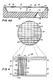
- the two-piece printhead of this invention is made possible by specially configured "V" grooves 29 anisotropically etched between rows of heating elements 30, more fully described later.
- the grooved structure allows identical pieces 28 to be placed face-to-face in a self-aligning manner, interlocking their respective lands 31 and grooves 29 as shown in Figure 3, where an enlarged schematic isometric view is shown of the front face of this printhead 11 mounted on daughter board 19.
- the array of droplet emitting nozzles 27 is depicted. Though normally the number nozzles in a printhead number from 48 to 128 or more, for purpose of illustration six are shown.
- the tunnels or channels are formed by making the height of the lands 31 containing the heating elements less than the depth of the groove it fits into. Since each piece 28 contains heating elements 30 separated by grooves 29, the spaces between heating elements in one piece are filled with the lands of those of the second piece and visa versa.
- Such an arrangement provides the highest possible density of droplet emitting nozzles as well as adequate isolation of the channels to prevent cross talk; i.e., the inadvertent ink expulsion from nozzles adjacent the one associated with the channel having its heating element addressed with a current pulse.
- Printheads of this type can be mass produced at relatively low cost by standard silicon integrated circuit fabrication technologies. Assembly requires one non-critical step of placing two identical pieces face-to-face. Alignment and interlocking of the two pieces is automatic and precise. Standard sealing techniques, such as the use of adhesives, can be incorporated into the assembly process whenever needed.
- both confronting pieces 28 have the heating elements 30 and addressing electrodes 33 formed on the lands 31 between the grooves 29.
- the edge of the printhead with the nozzles 27 are shown, and near the opposite end of the channels formed by grooves 29, openings 34 (not shown in this Figure) at the bottom or apex 37 of the grooves communicate with a common manifold or reservoir 35.
- a respective one of the heating elements is positioned in each channel, formed by the grooves in one piece and the lands in the other piece.
- Concentric holes 51, 53 in the flexible board 50 and stiffener 52 respectively provide communication between the cartridge aperture (not shown) and the manifold 35.
- a similar recess in the other printhead piece is sealed to the daughter board when the printhead is permanently attached thereto, so that the reservoir in this half of the printhead must be filled via at least one passageway (not shown) between a channel in each of the respective pieces 28.
- a stiffener 52 is bonded on the opposite surface 57 of the flexible board 50, so that flexing of the flexible board is not possible in the stiffened region. Also, refer to Figure 11 discussed later.
- the printhead piece electrodes are wire-bonded to the intermediate electrodes on the flexible board.
- the stiffener 52 prevents the flexible board from flexing where the wire bonds are attached.
- the subassembly of printhead piece, flexible boad and stiffener are attached to the printhead piece already bonded to the daughter board, as explained above.
- the channel open ends opposite the nozzles are sealingly closed, except for at least one passageway (not shown) interconnecting at least a respective one of the channels in each of the printhead pieces.
- any typical prior art method of sealing the channel ends will suffice, such as by using a thermosetting epoxy resin.
- the exposed and unused electrode 33 and heating element 30 on each printhead piece 28 may be removed by dicing or grinding for cosmetic purposes, but this operation is strictly optional, since the printhead functions perfectly as shown in Figure 3.
- the patterning of the grooves, heating elements, and electrodes could be designed to provide a balanced, symmetrical printhead without the need for the optional dicing step, but this would mean that the upper and lower pieces would not be identical.
- a plurality of pieces 28 may be produced from a two-side-polished, (100) silicon wafe 36, as shown in Figure 4.
- a pyrolytic CVD silicon nitride layer 41 is deposited on both sides.
- a via for the common reservoir recess 35 for each of the plurality of pieces 28 are printed at predetermined locations on one side 42 of wafer 36, opposite the side shown in Figure 4.
- the silicon nitride is plasma etched off of the patterns vias representing the recesses 35.
- a potassium hydroxide (KOH) anisotropic etch is used to etch the recesses.
- the ⁇ 111 ⁇ planes of the (100) wafer make an angle of 54.7 degrees with the surface 42 of the wafer.
- the width of the elongated recesses 35 are about 0.5mm, thus the recesses are etched to a terminating apex about half way to three quarters through the wafer.
- the relatively narrow recess is invarient to further size increase with continued etching, so that the recesses are not significantly time constrained. This etching takes about two hours and many wafers can be simultaneously processed.
- the opposite side 43 of wafer 36 is photolithographically patterned to form a plurality of set of resistive material deposits that will serve as the sets of heating elements 30, such as, for example, ZrB2.
- the resistive material may be doped polycrystalline silicon which may be deposited by chemical vapor deposition (CVD), in which case the silicon nitride layer on this side of the wafer may be optionally replaced with a coating or underglaze layer, such as SiO2, having a thickness of between 500 nm and 1 ⁇ m.
- the addressing electrodes 33 are aluminum leads deposited on the underglaze layer or silicon nitride and over the edges of the heating elements as shown in Figures 4A, 5 and 6.
- the electrodes 33 are deposited to a thickness of 0.5 to 3.0 ⁇ m, with the preferred thickness being 1.5 ⁇ m.
- a 2 micron thick phosphorous doped CVD SiO2 film (not shown) is deposited over the entire plurality of sets of heating elements and addressing electrodes and subsequently etched off of the terminal ends for later connection with the daughter board electrodes and common return, deposited later. This etching may be by either the wet or dry etching method. Alternatively, the electrode passivation may be accomplished by plasma deposited Si3N4.
- polysilicon heating elements may be subsequently oxidized in steam or oxygen at a relatively high temperature of about 1100°C for 50 to 80 minutes, prior to the deposition of the aluminum leads, in order to convert a small fraction of the polysilicon to SiO2.
- the heating elements are thermally oxidized to achieve an overglaze (not shown) of SiO2 of about 50 nm to 1 ⁇ m which has good integrity with substantially no pin holes.
- the thermally grown overglaze is removed from the opposing edges of polysilicon heating elements for attachment of the later deposited electrodes.
- the portion of the electrode passivation layer over the resistive material and associated thermal oxide layer is removed concurrently with its removal from the electrode terminals.
- a tantalum (Ta) layer may optionally be deposited to a thickness of about 1 ⁇ m on the oxidized polysilicon overglaze or passivation layer covering the heating elements for added protection thereof against the cavitational forces generated by the collapsing ink vapor bubbles during the printhead operation.
- the Ta layer is etched off all but the heating elements using, for example, CF4/O2 plasma etching.
- a plurality of sets of parallel strips of the wafer surface coating 41 and electrode heating element passivation layer are photolithographically patterned and removed to expose the wafer surface 43 between the rows of heating elements and electrodes.
- the surface coating 41 and passivation layer are removed by techniques well known in the art to obtain walls having sloping edges 46 with the exposed wafer surface 43.
- the two identical printhead pieces 28 fit more tightly together when their protective layers have sloping edges.
- the vias in the nitride and/or other passivation layers have a length longer than the desired subsequent ink channels and a width of 25 to 100 ⁇ m.
- Anisotropic etching of (100) silicon wafers must always be conducted through square or rectangular vias, so that the etching is along the ⁇ 111 ⁇ planes.
- each recess produced by the etching has walls at 54.7 degrees with the wafer surface, and if the vias are small enough with respect to the wafer thickness, V-grooves are formed instead of openings therethrough.
- the etching process stops at the intersection of the recess walls at apex 37.
- the depth of this apex from the wafer surface 43 is designed to slightly intersect the V-groove bottom of the reservoir recess 35, so that openings 34 are formed in each V-groove or channel 29, thus forming a common reservoir or manifold 35 for the channels of each printhead piece.
- Figures 5 and 6 depicting a printhead piece 28 having only four heating elements with addressing electrodes and three channels.
- Figure 5 shows the vias 38 between the heating elements 30 and aluminum electrodes 33 which expose the wafer surface 43.
- Figure 6 shows the printhead piece 28 after the anisotropic etching that produced the V-groove recess channels 29 and after the dicing cuts along the planes or lines 44 and 45, shown in dashed line in Figure 5, to open the end of the channels that will ultimately function as nozzles and to divide the pieces 28 at the bottom of one of the grooves 29.
- the silicon nitride layer 41 on which the heating elements and electrodes are formed act as an etch mask to define the position of the vias for channel recesses 29. Depth of the etch is controlled, as stated earlier, by the width of the vias or the nitride layer stripes.
- Heating elements spaced a predetermined distance from the printhead piece face 47 are connected to a common return 40 which may be, for example, formed on the entire printhead face 44a by omni-directional sputtering (i.e., sputtering in all directions on surface 44a) of a metal such as aluminum. The placement of such a common return must be accomplished without blocking or obstructing the channel open end which will eventually act as nozzles 27, see Figure 3.
- the common return 40 is then covered by a passivating layer (not shown) to protect it from the ink, after the wire bond 58 is in place.
- Wire bonds or beam leads formed at the far end of the addressing electrodes can be terminated at a flexboard strip line or at an attached edge connector, either of which may then be wire-bonded to the daughter board electrodes.
- a single-side-polished, (100) wafer may be used if the common ink reservoir 35 may be placed orthogonal to the V-groove channels 29 from the same side. Such may be accomplished by first etching the common reservoir and then filling it with polysilicon glass (PSG) prior to the heater formation (not shown). Upon completion of the body fabrication, the PSG can be etched out to join the reservoir to each channel. The addressing electrodes 33 fabricated over the PSG will bridge across the reservoir.
- PSG polysilicon glass
- a printhead of any desired length can be assembled from the printhead pieces 28 without loss of center-to-center spacing between nozzles 27. This is done by offsetting the first two pieces 28 which normally form a printhead by a predetermined number of channel grooves 29. Subsequent pieces added to the offset regions will self-align and abut together as shown by combining printhead pieces 28a, 28b, 28c, 28d, 28e, etc.
- the printhead pieces are depicted as having four heating elements and three grooves for simplicity and ease of understanding, while commercial embodiments generally have at least 48 channels or nozzles.
- a pagewidth printhead may be provided which may be held stationary, while the recording medium moves thereby at a constant velocity, during the printing operation, and in a direction perpendicular to the linear array of nozzles.
- One major advantage of pagewidth printing is that the speed of printing is greatly increased, since the recording medium does not have to be held stationary as is required by carriage-type printers.
- pagewidth printers as shown in Figure 7, may be stacked, each using a different colored ink from separate ink reservoirs (not shown).
- FIG. 8 An alternative embodiment is shown in Figures 8, 9 and 10 where parts identical with the embodiment of Figures 3, 5 and 6 have the same index numerals and similar parts have the same numerals but have the subscript "a.”
- integral ink supplying tunnels are formed during the V-groove anisotropic etching step by defining the insulating nitride layer stripes holding the heating elements 30 and addressing electrodes 33 such that each has a reduced width portion 61. This produces a depression 62 in each side wall of the V-grooves 29.
- the depressions 62 are aligned to form ink tunnels which interconnect open portions of V-groove channels in a continuous manner across the width of the printhead.
- the integral ink tunnel is terminated either by excluding the depression 62 from the outermost V-grooves 29 or by sealing the outer tunnels openings with a sealant such as epoxy (not shown).
- Ink may be fed to the printhead via one of these outer tunnel openings by, for example, a tube (not shown) or by a recess 35a anisotropically etched into the printhead piece 28 such that its apex opens at inlet 34a into one of the V-grooves 29.
- this alternative embodiment of Figures 8 to 10 is produced, fabricated and operated in the same way as the embodiment of Figures 1 through 7.
- Figures 11, 12 and 13 depict one way to assemble the two identical printhead pieces 28 or 28a, mount them on the daughter board 19, and wire bond them to the daughter board electrodes 23.
- the addressing electrodes 33 and common return 40 are wire-bonded to the nearer ends 48 of the daughter board electrode 23.
- one of the printhead pieces 28 is bonded to surface 54 to a T-shaped flexible board 50 such as, for example, Kapton ⁇ having intermediate electrodes 55 on one portion.
- a stiffener 52 is bonded on the opposite flexible board surface 57 to sandwich a portion of the flexible board 50 between the stiffener and the printhead piece.
- the stiffener prevents the flexible boad from flexing in the vicinity of the ends of the intermediate electrodes adjacent the printhead piece.
- the printhead electrodes 33 and common return 40 are wire-bonded to the adjacent ends of the intermediate electrodes 55 and the stiffener prevents debonding of the wire bonds 58, 59 because the flexible board cannot bend or twist in the vicinity of them.
- the sub-assembly comprising the printhead piece, flexible board and stiffener is mated to the printhead piece bonded to the daughter board with the lands of one printhead piece having the heating elements and addressing electrodes meshed into the V-grooves of the other printhead piece.
- the mated printhead pieces are bonded together and the cantilevered portion 56 of the flexible board moved toward daughter board, so that appropriate daughter board electrode terminals 49 are in electrical contact with the intermediate electrodes 55 on the flexible board whereat they are bonded together. All of the electrodes are passivated and the wire bonds 59 are encased in an electrical insulative material such as epoxy.
- a hole 51 in the flexible board and in hole 53 in the stiffener are aligned with the elongated reservoir 35 ( Figure 3) or hole 35a ( Figure 8). As explained earlier, these holes 51, 53 are sealingly connected to the aperture of the ink supply cartridge 12.
- the above described invention could be used for a continuous stream ink jet printer by using the bubbles generated by the heating elements as a means for perturbing the ink that would be continually streaming from the nozzles in order to break the streams into droplets a fixed distance from the nozzles, whereat charging electrodes would place a charge on the droplets according to its impact location on the recording medium or whether the droplet should be directed to a collecting gutter for recirculation. All changes required to modify this inventive printhead for continuous stream ink jet printing are well known from the prior art.
Applications Claiming Priority (2)
| Application Number | Priority Date | Filing Date | Title |
|---|---|---|---|
| US760009 | 1985-07-29 | ||
| US06/760,009 US4612554A (en) | 1985-07-29 | 1985-07-29 | High density thermal ink jet printhead |
Publications (3)
| Publication Number | Publication Date |
|---|---|
| EP0214733A2 true EP0214733A2 (fr) | 1987-03-18 |
| EP0214733A3 EP0214733A3 (en) | 1988-08-31 |
| EP0214733B1 EP0214733B1 (fr) | 1991-10-30 |
Family
ID=25057768
Family Applications (1)
| Application Number | Title | Priority Date | Filing Date |
|---|---|---|---|
| EP86305645A Expired - Lifetime EP0214733B1 (fr) | 1985-07-29 | 1986-07-23 | Tête d'impression thermique à jet d'encre de haute résolution |
Country Status (4)
| Country | Link |
|---|---|
| US (1) | US4612554A (fr) |
| EP (1) | EP0214733B1 (fr) |
| JP (1) | JPH0717064B2 (fr) |
| DE (1) | DE3682245D1 (fr) |
Cited By (3)
| Publication number | Priority date | Publication date | Assignee | Title |
|---|---|---|---|---|
| EP0533506A2 (fr) * | 1991-09-19 | 1993-03-24 | Brother Kogyo Kabushiki Kaisha | Dispositif à éjection de gouttelettes d'encre |
| EP0605006A2 (fr) * | 1993-01-01 | 1994-07-06 | Canon Kabushiki Kaisha | Tête d'éjection de liquide, appareil à éjection de liquide et sa méthode de fabrication |
| US5842258A (en) * | 1994-01-04 | 1998-12-01 | Xaar Technology Limited | Manufacture of ink jet printheads |
Families Citing this family (76)
| Publication number | Priority date | Publication date | Assignee | Title |
|---|---|---|---|---|
| USRE32572E (en) * | 1985-04-03 | 1988-01-05 | Xerox Corporation | Thermal ink jet printhead and process therefor |
| US4827294A (en) * | 1985-11-22 | 1989-05-02 | Hewlett-Packard Company | Thermal ink jet printhead assembly employing beam lead interconnect circuit |
| US4736213A (en) * | 1986-12-22 | 1988-04-05 | Eastman Kodak Company | Multiple print/cartridge ink jet printer having accurate vertical interpositioning |
| US4786357A (en) * | 1987-11-27 | 1988-11-22 | Xerox Corporation | Thermal ink jet printhead and fabrication method therefor |
| US4829324A (en) * | 1987-12-23 | 1989-05-09 | Xerox Corporation | Large array thermal ink jet printhead |
| JPH01255550A (ja) * | 1988-04-06 | 1989-10-12 | Ricoh Co Ltd | 液体噴射記録ヘッド |
| US4822755A (en) * | 1988-04-25 | 1989-04-18 | Xerox Corporation | Method of fabricating large area semiconductor arrays |
| GB8810241D0 (en) * | 1988-04-29 | 1988-06-02 | Am Int | Drop-on-demand printhead |
| DE68910015T2 (de) * | 1988-06-17 | 1994-05-05 | Ngk Insulators Ltd | Struktur mit detailliertem Muster und Herstellungsverfahren. |
| US4863560A (en) * | 1988-08-22 | 1989-09-05 | Xerox Corp | Fabrication of silicon structures by single side, multiple step etching process |
| JPH0267140A (ja) * | 1988-09-01 | 1990-03-07 | Ricoh Co Ltd | 液体噴射記録ヘッド |
| US4851371A (en) * | 1988-12-05 | 1989-07-25 | Xerox Corporation | Fabricating process for large array semiconductive devices |
| WO1990006853A1 (fr) * | 1988-12-14 | 1990-06-28 | Siemens Aktiengesellschaft | Procede pour l'optimisation d'une configuration de traces conducteurs pour tete d'ecriture dans des imprimantes a jet d'encre et configuration de traces conducteurs pour ladite tete d'ecriture |
| WO1990006852A1 (fr) * | 1988-12-14 | 1990-06-28 | Siemens Aktiengesellschaft | Dispositif servant a chauffer l'encre dans la tete d'ecriture d'une imprimante a encre |
| ES2067663T3 (es) * | 1989-03-01 | 1995-04-01 | Canon Kk | Substrato para impresion termica y cabezal para impresion termica que lo utiliza. |
| US4961821A (en) * | 1989-11-22 | 1990-10-09 | Xerox Corporation | Ode through holes and butt edges without edge dicing |
| US5000811A (en) * | 1989-11-22 | 1991-03-19 | Xerox Corporation | Precision buttable subunits via dicing |
| GB9010289D0 (en) * | 1990-05-08 | 1990-06-27 | Xaar Ltd | Drop-on-demand printing apparatus and method of manufacture |
| US5097274A (en) * | 1990-06-18 | 1992-03-17 | Xerox Corporation | Overlapping chip replaceable subunits, methods of making same, and methods of making RIS or ROS array bars incorporating these subunits |
| US5079189A (en) * | 1990-06-18 | 1992-01-07 | Xerox Corporation | Method of making RIS or ROS array bars using replaceable subunits |
| US5057854A (en) * | 1990-06-26 | 1991-10-15 | Xerox Corporation | Modular partial bars and full width array printheads fabricated from modular partial bars |
| ES2082145T3 (es) * | 1990-08-03 | 1996-03-16 | Canon Kk | Metodo para la fabricacion de un cabezal para la impresion por chorros de tinta. |
| US5136310A (en) * | 1990-09-28 | 1992-08-04 | Xerox Corporation | Thermal ink jet nozzle treatment |
| US5258781A (en) * | 1992-04-08 | 1993-11-02 | Xerox Corporation | One-step encapsulation, air gap sealing and structure bonding of thermal ink jet printhead |
| US5515089A (en) * | 1992-12-08 | 1996-05-07 | Xerox Corporation | Ink jet printhead with sealed manifold and printhead die |
| US5308442A (en) * | 1993-01-25 | 1994-05-03 | Hewlett-Packard Company | Anisotropically etched ink fill slots in silicon |
| US5387314A (en) * | 1993-01-25 | 1995-02-07 | Hewlett-Packard Company | Fabrication of ink fill slots in thermal ink-jet printheads utilizing chemical micromachining |
| US5487334A (en) * | 1993-02-25 | 1996-01-30 | Matthews International Corporation | Apparatus for producing characters on a product |
| US5388326A (en) * | 1993-09-07 | 1995-02-14 | Hewlett-Packard Corporation | Self aligning orifice construction for thermal ink-jet printheads |
| JPH07186388A (ja) * | 1993-11-22 | 1995-07-25 | Xerox Corp | 大規模配列インク・ジェット・プリントヘッドおよびその製造方法 |
| US5457879A (en) * | 1994-01-04 | 1995-10-17 | Motorola, Inc. | Method of shaping inter-substrate plug and receptacles interconnects |
| FR2727648B1 (fr) * | 1994-12-01 | 1997-01-03 | Commissariat Energie Atomique | Procede de fabrication micromecanique de buses pour jets de liquide |
| US6135586A (en) * | 1995-10-31 | 2000-10-24 | Hewlett-Packard Company | Large area inkjet printhead |
| EP0910478A4 (fr) * | 1996-07-08 | 1999-09-01 | Corning Inc | Dispositifs d'atomisation a rupture de rayleigh et procedes de fabrication de ces dispositifs |
| US6352209B1 (en) | 1996-07-08 | 2002-03-05 | Corning Incorporated | Gas assisted atomizing devices and methods of making gas-assisted atomizing devices |
| CN1226960A (zh) | 1996-07-08 | 1999-08-25 | 康宁股份有限公司 | 气体助推式雾化装置 |
| US5870123A (en) * | 1996-07-15 | 1999-02-09 | Xerox Corporation | Ink jet printhead with channels formed in silicon with a (110) surface orientation |
| US5901425A (en) | 1996-08-27 | 1999-05-11 | Topaz Technologies Inc. | Inkjet print head apparatus |
| US5923348A (en) * | 1997-02-26 | 1999-07-13 | Lexmark International, Inc. | Method of printing using a printhead having multiple rows of ink emitting orifices |
| US6393685B1 (en) * | 1997-06-10 | 2002-05-28 | The Regents Of The University Of California | Microjoinery methods and devices |
| US7465030B2 (en) | 1997-07-15 | 2008-12-16 | Silverbrook Research Pty Ltd | Nozzle arrangement with a magnetic field generator |
| US6712453B2 (en) | 1997-07-15 | 2004-03-30 | Silverbrook Research Pty Ltd. | Ink jet nozzle rim |
| US7468139B2 (en) | 1997-07-15 | 2008-12-23 | Silverbrook Research Pty Ltd | Method of depositing heater material over a photoresist scaffold |
| US6935724B2 (en) | 1997-07-15 | 2005-08-30 | Silverbrook Research Pty Ltd | Ink jet nozzle having actuator with anchor positioned between nozzle chamber and actuator connection point |
| US7195339B2 (en) | 1997-07-15 | 2007-03-27 | Silverbrook Research Pty Ltd | Ink jet nozzle assembly with a thermal bend actuator |
| US7337532B2 (en) | 1997-07-15 | 2008-03-04 | Silverbrook Research Pty Ltd | Method of manufacturing micro-electromechanical device having motion-transmitting structure |
| US20100225698A1 (en) * | 1997-07-15 | 2010-09-09 | Silverbrook Research Pty Ltd. | Pagewidth printer with movable capping member for printhead |
| US6648453B2 (en) | 1997-07-15 | 2003-11-18 | Silverbrook Research Pty Ltd | Ink jet printhead chip with predetermined micro-electromechanical systems height |
| US6682174B2 (en) | 1998-03-25 | 2004-01-27 | Silverbrook Research Pty Ltd | Ink jet nozzle arrangement configuration |
| US6641315B2 (en) * | 1997-07-15 | 2003-11-04 | Silverbrook Research Pty Ltd | Keyboard |
| US6948794B2 (en) * | 1997-07-15 | 2005-09-27 | Silverbrook Reserach Pty Ltd | Printhead re-capping assembly for a print and demand digital camera system |
| US7556356B1 (en) | 1997-07-15 | 2009-07-07 | Silverbrook Research Pty Ltd | Inkjet printhead integrated circuit with ink spread prevention |
| US6188415B1 (en) | 1997-07-15 | 2001-02-13 | Silverbrook Research Pty Ltd | Ink jet printer having a thermal actuator comprising an external coil spring |
| US6733116B1 (en) * | 1998-10-16 | 2004-05-11 | Silverbrook Research Pty Ltd | Ink jet printer with print roll and printhead assemblies |
| US6508546B2 (en) * | 1998-10-16 | 2003-01-21 | Silverbrook Research Pty Ltd | Ink supply arrangement for a portable ink jet printer |
| US6449831B1 (en) * | 1998-06-19 | 2002-09-17 | Lexmark International, Inc | Process for making a heater chip module |
| JP2002527272A (ja) | 1998-10-16 | 2002-08-27 | シルバーブルック リサーチ プロプライエタリイ、リミテッド | インクジェットプリンタに関する改良 |
| US7216956B2 (en) * | 1998-10-16 | 2007-05-15 | Silverbrook Research Pty Ltd | Printhead assembly with power and ground connections along single edge |
| US6183063B1 (en) | 1999-03-04 | 2001-02-06 | Lexmark International, Inc. | Angled printer cartridge |
| US6503359B2 (en) * | 1999-03-05 | 2003-01-07 | Burstein Technologies, Inc. | Monomolecular adhesion methods for manufacturing microfabricated multilaminate devices |
| US6592204B1 (en) | 1999-03-26 | 2003-07-15 | Spectra, Inc. | Single-pass inkjet printing |
| US6575558B1 (en) | 1999-03-26 | 2003-06-10 | Spectra, Inc. | Single-pass inkjet printing |
| AU2004202968B2 (en) * | 2001-01-30 | 2005-06-30 | Zamtec Limited | Inkjet printhead having nozzle guard with formations for proper alignment |
| AUPR277701A0 (en) * | 2001-01-30 | 2001-02-22 | Silverbrook Research Pty. Ltd. | An apparatus (art98) |
| US6863833B1 (en) * | 2001-06-29 | 2005-03-08 | The Board Of Trustees Of The Leland Stanford Junior University | Microfabricated apertures for supporting bilayer lipid membranes |
| US6793334B2 (en) * | 2002-04-11 | 2004-09-21 | Hewlett-Packard Development Company, L.P. | Barcode printing module |
| US7431427B2 (en) * | 2002-06-13 | 2008-10-07 | Silverbrook Research Pty Ltd | Ink supply arrangement with improved ink flows |
| WO2004094069A1 (fr) * | 2003-04-11 | 2004-11-04 | Nordson Corporation | Buse de pulverisation sans air |
| US20050133480A1 (en) * | 2003-12-19 | 2005-06-23 | Xerox Corporation | Methods for making internal die filters with multiple passageways which are fluidically in parallel |
| JP4182921B2 (ja) * | 2004-06-08 | 2008-11-19 | セイコーエプソン株式会社 | ノズルプレートの製造方法 |
| US7160052B2 (en) * | 2004-08-24 | 2007-01-09 | The United States Of America As Represented By The Secretary Of The Army | Paving system using arrays of vertically interlocking paving blocks |
| JP4605760B2 (ja) * | 2004-11-08 | 2011-01-05 | キヤノン株式会社 | 発熱抵抗体膜の製造方法、記録ヘッド用基体の製造方法 |
| US7419327B2 (en) * | 2006-11-22 | 2008-09-02 | The United States Of America As Represented By The Secretary Of The Army | Method for fabricating and employing a paving system using arrays of vertically interlocking paving blocks |
| US20080158327A1 (en) * | 2007-01-03 | 2008-07-03 | Robert P. Siegel | Portable system for large area printing |
| US20100154190A1 (en) * | 2008-12-19 | 2010-06-24 | Sanger Kurt M | Method of making a composite device |
| US9604459B2 (en) | 2014-12-15 | 2017-03-28 | Hewlett-Packard Development Company, L.P. | Multi-part printhead assembly |
Citations (2)
| Publication number | Priority date | Publication date | Assignee | Title |
|---|---|---|---|---|
| US4314259A (en) * | 1980-06-16 | 1982-02-02 | Arthur D. Little, Inc. | Apparatus for providing an array of fine liquid droplets particularly suited for ink-jet printing |
| EP0100624A1 (fr) * | 1982-07-30 | 1984-02-15 | Hewlett-Packard Company | Imprimante à jet d'encre avec une membrane flexible entraînée par bulle de vapeur |
Family Cites Families (12)
| Publication number | Priority date | Publication date | Assignee | Title |
|---|---|---|---|---|
| US4216477A (en) * | 1978-05-10 | 1980-08-05 | Hitachi, Ltd. | Nozzle head of an ink-jet printing apparatus with built-in fluid diodes |
| JPS585785B2 (ja) * | 1978-05-10 | 1983-02-01 | 株式会社日立製作所 | インクジエツト記録用ノズルヘツド |
| JPS6043308B2 (ja) * | 1978-10-06 | 1985-09-27 | 富士ゼロックス株式会社 | マルチノズルオリフイス板の作成方法 |
| JPS6043309B2 (ja) * | 1978-10-06 | 1985-09-27 | 富士ゼロックス株式会社 | マルチノズルオリフイス板 |
| US4335389A (en) * | 1979-03-27 | 1982-06-15 | Canon Kabushiki Kaisha | Liquid droplet ejecting recording head |
| JPS55129472A (en) * | 1979-03-29 | 1980-10-07 | Canon Inc | Method of adhesion |
| DE3011919A1 (de) * | 1979-03-27 | 1980-10-09 | Canon Kk | Verfahren zur herstellung eines aufzeichnungskopfes |
| US4463359A (en) * | 1979-04-02 | 1984-07-31 | Canon Kabushiki Kaisha | Droplet generating method and apparatus thereof |
| US4417251A (en) * | 1980-03-06 | 1983-11-22 | Canon Kabushiki Kaisha | Ink jet head |
| US4377814A (en) * | 1981-04-17 | 1983-03-22 | Xerox Corporation | Ink jet printing machine |
| US4438191A (en) * | 1982-11-23 | 1984-03-20 | Hewlett-Packard Company | Monolithic ink jet print head |
| US4571599A (en) * | 1984-12-03 | 1986-02-18 | Xerox Corporation | Ink cartridge for an ink jet printer |
-
1985
- 1985-07-29 US US06/760,009 patent/US4612554A/en not_active Expired - Fee Related
-
1986
- 1986-07-22 JP JP61172663A patent/JPH0717064B2/ja not_active Expired - Lifetime
- 1986-07-23 DE DE8686305645T patent/DE3682245D1/de not_active Expired - Fee Related
- 1986-07-23 EP EP86305645A patent/EP0214733B1/fr not_active Expired - Lifetime
Patent Citations (2)
| Publication number | Priority date | Publication date | Assignee | Title |
|---|---|---|---|---|
| US4314259A (en) * | 1980-06-16 | 1982-02-02 | Arthur D. Little, Inc. | Apparatus for providing an array of fine liquid droplets particularly suited for ink-jet printing |
| EP0100624A1 (fr) * | 1982-07-30 | 1984-02-15 | Hewlett-Packard Company | Imprimante à jet d'encre avec une membrane flexible entraînée par bulle de vapeur |
Non-Patent Citations (1)
| Title |
|---|
| IBM TECHNICAL DISCLOSURE BULLETIN, vol. 19, no. 6, November 1976, pages 2243-2246, New York, US; E. BASSOUS et al.: "Fabrication of dense arrays of nozzles and channels with high degree of precision" * |
Cited By (7)
| Publication number | Priority date | Publication date | Assignee | Title |
|---|---|---|---|---|
| EP0533506A2 (fr) * | 1991-09-19 | 1993-03-24 | Brother Kogyo Kabushiki Kaisha | Dispositif à éjection de gouttelettes d'encre |
| EP0533506A3 (fr) * | 1991-09-19 | 1993-06-02 | Brother Kogyo Kabushiki Kaisha | Dispositif à éjection de gouttelettes d'encre |
| EP0605006A2 (fr) * | 1993-01-01 | 1994-07-06 | Canon Kabushiki Kaisha | Tête d'éjection de liquide, appareil à éjection de liquide et sa méthode de fabrication |
| EP0605006A3 (en) * | 1993-01-01 | 1994-09-14 | Canon Kk | Liquid ejecting head, liquid ejecting apparatus and method of producing said liquid ejecting head. |
| US5774151A (en) * | 1993-01-01 | 1998-06-30 | Canon Kabushiki Kaisha | Liquid ejecting head, liquid ejecting apparatus and method of producing said liquid ejecting head |
| US5842258A (en) * | 1994-01-04 | 1998-12-01 | Xaar Technology Limited | Manufacture of ink jet printheads |
| EP1270232A2 (fr) | 1994-01-04 | 2003-01-02 | Xaar Technology Limited | Fabrication de têtes d'impression par jet d'encre |
Also Published As
| Publication number | Publication date |
|---|---|
| DE3682245D1 (de) | 1991-12-05 |
| JPS6255155A (ja) | 1987-03-10 |
| US4612554A (en) | 1986-09-16 |
| EP0214733A3 (en) | 1988-08-31 |
| EP0214733B1 (fr) | 1991-10-30 |
| JPH0717064B2 (ja) | 1995-03-01 |
Similar Documents
| Publication | Publication Date | Title |
|---|---|---|
| EP0214733B1 (fr) | Tête d'impression thermique à jet d'encre de haute résolution | |
| US4639748A (en) | Ink jet printhead with integral ink filter | |
| US4829324A (en) | Large array thermal ink jet printhead | |
| US4899181A (en) | Large monolithic thermal ink jet printhead | |
| EP0210848B1 (fr) | Tête d'impression thermique à jet d'encre | |
| EP0197723B1 (fr) | Tête d'impression thermique par projection d'encre et son procédé de fabrication | |
| US4774530A (en) | Ink jet printhead | |
| USRE32572E (en) | Thermal ink jet printhead and process therefor | |
| US4786357A (en) | Thermal ink jet printhead and fabrication method therefor | |
| US5041190A (en) | Method of fabricating channel plates and ink jet printheads containing channel plates | |
| US4899178A (en) | Thermal ink jet printhead with internally fed ink reservoir | |
| EP0430692B1 (fr) | Méthode de fabrication de tête d'impression | |
| US5132707A (en) | Ink jet printhead | |
| US5160577A (en) | Method of fabricating an aperture plate for a roof-shooter type printhead | |
| US5017941A (en) | Thermal ink jet printhead with recirculating cooling system | |
| US5278585A (en) | Ink jet printhead with ink flow directing valves | |
| EP0438295B1 (fr) | Têtes d'impression à jet d'encre thermiques | |
| US5870123A (en) | Ink jet printhead with channels formed in silicon with a (110) surface orientation | |
| US6079819A (en) | Ink jet printhead having a low cross talk ink channel structure | |
| US4835553A (en) | Thermal ink jet printhead with increased drop generation rate | |
| US5461406A (en) | Method and apparatus for elimination of misdirected satellite drops in thermal ink jet printhead | |
| JP3564864B2 (ja) | インクジェットヘッドの製造方法 |
Legal Events
| Date | Code | Title | Description |
|---|---|---|---|
| PUAI | Public reference made under article 153(3) epc to a published international application that has entered the european phase |
Free format text: ORIGINAL CODE: 0009012 |
|
| AK | Designated contracting states |
Kind code of ref document: A2 Designated state(s): DE FR GB |
|
| PUAL | Search report despatched |
Free format text: ORIGINAL CODE: 0009013 |
|
| AK | Designated contracting states |
Kind code of ref document: A3 Designated state(s): DE FR GB |
|
| 17P | Request for examination filed |
Effective date: 19890215 |
|
| R17P | Request for examination filed (corrected) |
Effective date: 19890215 |
|
| 17Q | First examination report despatched |
Effective date: 19900521 |
|
| GRAA | (expected) grant |
Free format text: ORIGINAL CODE: 0009210 |
|
| AK | Designated contracting states |
Kind code of ref document: B1 Designated state(s): DE FR GB |
|
| REF | Corresponds to: |
Ref document number: 3682245 Country of ref document: DE Date of ref document: 19911205 |
|
| ET | Fr: translation filed | ||
| PLBE | No opposition filed within time limit |
Free format text: ORIGINAL CODE: 0009261 |
|
| STAA | Information on the status of an ep patent application or granted ep patent |
Free format text: STATUS: NO OPPOSITION FILED WITHIN TIME LIMIT |
|
| 26N | No opposition filed | ||
| PGFP | Annual fee paid to national office [announced via postgrant information from national office to epo] |
Ref country code: FR Payment date: 19970709 Year of fee payment: 12 |
|
| PGFP | Annual fee paid to national office [announced via postgrant information from national office to epo] |
Ref country code: GB Payment date: 19970714 Year of fee payment: 12 |
|
| PGFP | Annual fee paid to national office [announced via postgrant information from national office to epo] |
Ref country code: DE Payment date: 19970801 Year of fee payment: 12 |
|
| PG25 | Lapsed in a contracting state [announced via postgrant information from national office to epo] |
Ref country code: GB Free format text: LAPSE BECAUSE OF NON-PAYMENT OF DUE FEES Effective date: 19980723 |
|
| GBPC | Gb: european patent ceased through non-payment of renewal fee |
Effective date: 19980723 |
|
| PG25 | Lapsed in a contracting state [announced via postgrant information from national office to epo] |
Ref country code: FR Free format text: LAPSE BECAUSE OF NON-PAYMENT OF DUE FEES Effective date: 19990331 |
|
| PG25 | Lapsed in a contracting state [announced via postgrant information from national office to epo] |
Ref country code: DE Free format text: LAPSE BECAUSE OF NON-PAYMENT OF DUE FEES Effective date: 19990501 |
|
| REG | Reference to a national code |
Ref country code: FR Ref legal event code: ST |