EP0213910B1 - Method of manufacturing a semiconductor device free from the current leakage through a semi-conductor layer - Google Patents
Method of manufacturing a semiconductor device free from the current leakage through a semi-conductor layer Download PDFInfo
- Publication number
- EP0213910B1 EP0213910B1 EP86306556A EP86306556A EP0213910B1 EP 0213910 B1 EP0213910 B1 EP 0213910B1 EP 86306556 A EP86306556 A EP 86306556A EP 86306556 A EP86306556 A EP 86306556A EP 0213910 B1 EP0213910 B1 EP 0213910B1
- Authority
- EP
- European Patent Office
- Prior art keywords
- semiconductor layer
- electrode
- layer
- semiconductor
- voltage
- Prior art date
- Legal status (The legal status is an assumption and is not a legal conclusion. Google has not performed a legal analysis and makes no representation as to the accuracy of the status listed.)
- Expired - Lifetime
Links
- 239000004065 semiconductor Substances 0.000 title claims description 66
- 238000004519 manufacturing process Methods 0.000 title claims description 14
- 238000000034 method Methods 0.000 claims description 41
- 239000011347 resin Substances 0.000 claims description 27
- 229920005989 resin Polymers 0.000 claims description 27
- 239000000758 substrate Substances 0.000 claims description 18
- 239000004411 aluminium Substances 0.000 claims description 17
- 229910052782 aluminium Inorganic materials 0.000 claims description 17
- XAGFODPZIPBFFR-UHFFFAOYSA-N aluminium Chemical compound [Al] XAGFODPZIPBFFR-UHFFFAOYSA-N 0.000 claims description 17
- XOLBLPGZBRYERU-UHFFFAOYSA-N tin dioxide Chemical compound O=[Sn]=O XOLBLPGZBRYERU-UHFFFAOYSA-N 0.000 claims description 11
- 230000015556 catabolic process Effects 0.000 claims description 10
- 239000000463 material Substances 0.000 claims description 8
- 239000000203 mixture Substances 0.000 claims description 7
- 230000015572 biosynthetic process Effects 0.000 claims description 5
- 239000011521 glass Substances 0.000 claims description 5
- VYZAMTAEIAYCRO-UHFFFAOYSA-N Chromium Chemical compound [Cr] VYZAMTAEIAYCRO-UHFFFAOYSA-N 0.000 claims description 4
- 229910052804 chromium Inorganic materials 0.000 claims description 4
- 239000011651 chromium Substances 0.000 claims description 4
- 150000001875 compounds Chemical class 0.000 claims description 4
- PJXISJQVUVHSOJ-UHFFFAOYSA-N indium(III) oxide Inorganic materials [O-2].[O-2].[O-2].[In+3].[In+3] PJXISJQVUVHSOJ-UHFFFAOYSA-N 0.000 claims description 4
- 229910052751 metal Inorganic materials 0.000 claims description 4
- 239000002184 metal Substances 0.000 claims description 4
- BQCADISMDOOEFD-UHFFFAOYSA-N Silver Chemical compound [Ag] BQCADISMDOOEFD-UHFFFAOYSA-N 0.000 claims description 3
- 238000011049 filling Methods 0.000 claims description 3
- 229910052709 silver Inorganic materials 0.000 claims description 3
- 239000004332 silver Substances 0.000 claims description 3
- 239000004020 conductor Substances 0.000 claims 1
- 238000006731 degradation reaction Methods 0.000 claims 1
- 239000010410 layer Substances 0.000 description 75
- 239000010408 film Substances 0.000 description 18
- 229920002120 photoresistant polymer Polymers 0.000 description 10
- 230000007547 defect Effects 0.000 description 7
- 239000010409 thin film Substances 0.000 description 7
- 238000000059 patterning Methods 0.000 description 6
- XUIMIQQOPSSXEZ-UHFFFAOYSA-N Silicon Chemical compound [Si] XUIMIQQOPSSXEZ-UHFFFAOYSA-N 0.000 description 4
- 238000006243 chemical reaction Methods 0.000 description 4
- 229910052710 silicon Inorganic materials 0.000 description 4
- 239000010703 silicon Substances 0.000 description 4
- -1 tin nitride Chemical class 0.000 description 4
- 229910001887 tin oxide Inorganic materials 0.000 description 4
- 229910007675 Sn3N4 Inorganic materials 0.000 description 3
- 238000005229 chemical vapour deposition Methods 0.000 description 3
- 238000010586 diagram Methods 0.000 description 3
- 229910052736 halogen Inorganic materials 0.000 description 3
- 150000002367 halogens Chemical class 0.000 description 3
- 239000012212 insulator Substances 0.000 description 3
- 230000003993 interaction Effects 0.000 description 3
- 238000005268 plasma chemical vapour deposition Methods 0.000 description 3
- 238000004544 sputter deposition Methods 0.000 description 3
- PXHVJJICTQNCMI-UHFFFAOYSA-N Nickel Chemical compound [Ni] PXHVJJICTQNCMI-UHFFFAOYSA-N 0.000 description 2
- 229910021417 amorphous silicon Inorganic materials 0.000 description 2
- NWAIGJYBQQYSPW-UHFFFAOYSA-N azanylidyneindigane Chemical compound [In]#N NWAIGJYBQQYSPW-UHFFFAOYSA-N 0.000 description 2
- 230000004888 barrier function Effects 0.000 description 2
- 238000000151 deposition Methods 0.000 description 2
- 238000000313 electron-beam-induced deposition Methods 0.000 description 2
- 238000002474 experimental method Methods 0.000 description 2
- 239000011888 foil Substances 0.000 description 2
- 238000004518 low pressure chemical vapour deposition Methods 0.000 description 2
- 239000012044 organic layer Substances 0.000 description 2
- 238000009987 spinning Methods 0.000 description 2
- 238000005507 spraying Methods 0.000 description 2
- MARUHZGHZWCEQU-UHFFFAOYSA-N 5-phenyl-2h-tetrazole Chemical compound C1=CC=CC=C1C1=NNN=N1 MARUHZGHZWCEQU-UHFFFAOYSA-N 0.000 description 1
- JBRZTFJDHDCESZ-UHFFFAOYSA-N AsGa Chemical compound [As]#[Ga] JBRZTFJDHDCESZ-UHFFFAOYSA-N 0.000 description 1
- 239000004593 Epoxy Substances 0.000 description 1
- 229910001218 Gallium arsenide Inorganic materials 0.000 description 1
- 239000004952 Polyamide Substances 0.000 description 1
- 239000004642 Polyimide Substances 0.000 description 1
- 229910052581 Si3N4 Inorganic materials 0.000 description 1
- 229910020751 SixGe1-x Inorganic materials 0.000 description 1
- 238000010521 absorption reaction Methods 0.000 description 1
- 229910045601 alloy Inorganic materials 0.000 description 1
- 239000000956 alloy Substances 0.000 description 1
- 239000011195 cermet Substances 0.000 description 1
- 239000011248 coating agent Substances 0.000 description 1
- 238000000576 coating method Methods 0.000 description 1
- 238000007796 conventional method Methods 0.000 description 1
- 239000013256 coordination polymer Substances 0.000 description 1
- 239000013078 crystal Substances 0.000 description 1
- 230000003247 decreasing effect Effects 0.000 description 1
- 210000003298 dental enamel Anatomy 0.000 description 1
- 230000008021 deposition Effects 0.000 description 1
- 230000000694 effects Effects 0.000 description 1
- 230000005611 electricity Effects 0.000 description 1
- 238000005530 etching Methods 0.000 description 1
- 150000002472 indium compounds Chemical class 0.000 description 1
- 229910003437 indium oxide Inorganic materials 0.000 description 1
- 230000001678 irradiating effect Effects 0.000 description 1
- 229910021421 monocrystalline silicon Inorganic materials 0.000 description 1
- 229910052759 nickel Inorganic materials 0.000 description 1
- 150000004767 nitrides Chemical class 0.000 description 1
- 230000003647 oxidation Effects 0.000 description 1
- 238000007254 oxidation reaction Methods 0.000 description 1
- 238000005192 partition Methods 0.000 description 1
- 238000002161 passivation Methods 0.000 description 1
- 229920003223 poly(pyromellitimide-1,4-diphenyl ether) Polymers 0.000 description 1
- 229920002647 polyamide Polymers 0.000 description 1
- 229920001721 polyimide Polymers 0.000 description 1
- 238000011417 postcuring Methods 0.000 description 1
- 230000005855 radiation Effects 0.000 description 1
- HQVNEWCFYHHQES-UHFFFAOYSA-N silicon nitride Chemical compound N12[Si]34N5[Si]62N3[Si]51N64 HQVNEWCFYHHQES-UHFFFAOYSA-N 0.000 description 1
- 238000005245 sintering Methods 0.000 description 1
- 238000007669 thermal treatment Methods 0.000 description 1
- 150000003606 tin compounds Chemical class 0.000 description 1
- 238000007740 vapor deposition Methods 0.000 description 1
- XLYOFNOQVPJJNP-UHFFFAOYSA-N water Substances O XLYOFNOQVPJJNP-UHFFFAOYSA-N 0.000 description 1
Images


Classifications
-
- H—ELECTRICITY
- H01—ELECTRIC ELEMENTS
- H01L—SEMICONDUCTOR DEVICES NOT COVERED BY CLASS H10
- H01L31/00—Semiconductor devices sensitive to infrared radiation, light, electromagnetic radiation of shorter wavelength or corpuscular radiation and specially adapted either for the conversion of the energy of such radiation into electrical energy or for the control of electrical energy by such radiation; Processes or apparatus specially adapted for the manufacture or treatment thereof or of parts thereof; Details thereof
- H01L31/02—Details
- H01L31/0216—Coatings
- H01L31/02161—Coatings for devices characterised by at least one potential jump barrier or surface barrier
- H01L31/02167—Coatings for devices characterised by at least one potential jump barrier or surface barrier for solar cells
-
- H—ELECTRICITY
- H01—ELECTRIC ELEMENTS
- H01L—SEMICONDUCTOR DEVICES NOT COVERED BY CLASS H10
- H01L31/00—Semiconductor devices sensitive to infrared radiation, light, electromagnetic radiation of shorter wavelength or corpuscular radiation and specially adapted either for the conversion of the energy of such radiation into electrical energy or for the control of electrical energy by such radiation; Processes or apparatus specially adapted for the manufacture or treatment thereof or of parts thereof; Details thereof
- H01L31/04—Semiconductor devices sensitive to infrared radiation, light, electromagnetic radiation of shorter wavelength or corpuscular radiation and specially adapted either for the conversion of the energy of such radiation into electrical energy or for the control of electrical energy by such radiation; Processes or apparatus specially adapted for the manufacture or treatment thereof or of parts thereof; Details thereof adapted as photovoltaic [PV] conversion devices
- H01L31/042—PV modules or arrays of single PV cells
- H01L31/0445—PV modules or arrays of single PV cells including thin film solar cells, e.g. single thin film a-Si, CIS or CdTe solar cells
- H01L31/046—PV modules composed of a plurality of thin film solar cells deposited on the same substrate
-
- H—ELECTRICITY
- H01—ELECTRIC ELEMENTS
- H01L—SEMICONDUCTOR DEVICES NOT COVERED BY CLASS H10
- H01L31/00—Semiconductor devices sensitive to infrared radiation, light, electromagnetic radiation of shorter wavelength or corpuscular radiation and specially adapted either for the conversion of the energy of such radiation into electrical energy or for the control of electrical energy by such radiation; Processes or apparatus specially adapted for the manufacture or treatment thereof or of parts thereof; Details thereof
- H01L31/18—Processes or apparatus specially adapted for the manufacture or treatment of these devices or of parts thereof
- H01L31/20—Processes or apparatus specially adapted for the manufacture or treatment of these devices or of parts thereof such devices or parts thereof comprising amorphous semiconductor materials
- H01L31/208—Particular post-treatment of the devices, e.g. annealing, short-circuit elimination
-
- Y—GENERAL TAGGING OF NEW TECHNOLOGICAL DEVELOPMENTS; GENERAL TAGGING OF CROSS-SECTIONAL TECHNOLOGIES SPANNING OVER SEVERAL SECTIONS OF THE IPC; TECHNICAL SUBJECTS COVERED BY FORMER USPC CROSS-REFERENCE ART COLLECTIONS [XRACs] AND DIGESTS
- Y02—TECHNOLOGIES OR APPLICATIONS FOR MITIGATION OR ADAPTATION AGAINST CLIMATE CHANGE
- Y02E—REDUCTION OF GREENHOUSE GAS [GHG] EMISSIONS, RELATED TO ENERGY GENERATION, TRANSMISSION OR DISTRIBUTION
- Y02E10/00—Energy generation through renewable energy sources
- Y02E10/50—Photovoltaic [PV] energy
-
- Y—GENERAL TAGGING OF NEW TECHNOLOGICAL DEVELOPMENTS; GENERAL TAGGING OF CROSS-SECTIONAL TECHNOLOGIES SPANNING OVER SEVERAL SECTIONS OF THE IPC; TECHNICAL SUBJECTS COVERED BY FORMER USPC CROSS-REFERENCE ART COLLECTIONS [XRACs] AND DIGESTS
- Y02—TECHNOLOGIES OR APPLICATIONS FOR MITIGATION OR ADAPTATION AGAINST CLIMATE CHANGE
- Y02P—CLIMATE CHANGE MITIGATION TECHNOLOGIES IN THE PRODUCTION OR PROCESSING OF GOODS
- Y02P70/00—Climate change mitigation technologies in the production process for final industrial or consumer products
- Y02P70/50—Manufacturing or production processes characterised by the final manufactured product
-
- Y—GENERAL TAGGING OF NEW TECHNOLOGICAL DEVELOPMENTS; GENERAL TAGGING OF CROSS-SECTIONAL TECHNOLOGIES SPANNING OVER SEVERAL SECTIONS OF THE IPC; TECHNICAL SUBJECTS COVERED BY FORMER USPC CROSS-REFERENCE ART COLLECTIONS [XRACs] AND DIGESTS
- Y10—TECHNICAL SUBJECTS COVERED BY FORMER USPC
- Y10S—TECHNICAL SUBJECTS COVERED BY FORMER USPC CROSS-REFERENCE ART COLLECTIONS [XRACs] AND DIGESTS
- Y10S136/00—Batteries: thermoelectric and photoelectric
- Y10S136/29—Testing, calibrating, treating, e.g. aging
Definitions
- This invention relates to a method of manufacturing a semiconductor device in which the performance of the semiconductor device is improved. More particularly, this invention relates to measures for eliminating disadvantages caused by the effect of electrical shorts and shunts due to pinholes or other gaps created during the fabrication process of the device.
- a transparent conductive film 2 is formed on a glass substrate 1 with a mask aligned above the substrate 1.
- Semiconductor layers 3 are deposited on the substrate 1 with the conductive film 2 therebetween with a mask aligned above the substrate 1.
- aluminium layer 4 are formed as second electrodes with a mask.
- Reference numerals 31 and 11 designate photoelectric cells respectively in the figure.
- the two cells 31 and 11 are connected in series by means of a connection 12.
- the second electrode 38 is made in contact with the first electrode 37.
- a number of the cells are connected with each other in series.
- the integrated photovoltaic device tends to be degraded after thermal treatment at 150°C for tens of hours. Such device is not suitable for outdoor use where the device is likely to be subjected to high ambient temperature.
- the voltage and current output of thin film solar cells may be greatly reduced or completely eliminated by electrical shorts or shunts formed during the fabrication of the solar cell. Electrical shorts occur when there is a pinhole in the semiconductor layer and the front and back electrodes are touching. A shunt is the loss of charge in the semiconductor body due to imperfect barrier formation or the formation of an ohmic contact by a high work function metal rather than a Schottky barrier formation. The problem of solar cell defects which cause shorts or shunts increase greatly with increasing solar cell size. If large area solar cells are to be economically feasible, then methods of eliminating these shorts and shunts during fabrication or removing the defects after processing must be developed.
- US-A-4166918 a conventional method of improving the performance of a solar cell made from gallium arsenide, cadmium telluride, single crystal or amorphous silicon and the like requires the etching out of the defects in the solar cell, and attempts made to remove the defects by the application of a reverse bias voltage tended to increase the incidence of shorts and shunts in the solar cell.
- the proposal made in US-A-4166918 is for a method of improving the performance of a solar cell which incorporates a thick film cermet electrode contacting the active region of the solar cell opposite to a surface incident to solar radiation, the method comprising applying a reverse bias voltage of sufficient magnitude to burn out the defects in that solar cell but less than the breakdown voltage of the cell.
- EP-A-0060487 discloses a plugged pinhole thin film and a method of making the same which is said to be particularly useful in the production of thin film insulating or semiconductor layers and thin film devices such as photoconductive and photovoltaic devices.
- the thin film of EP-A-0060487 has its pinholes plugged with insoluble insulating photoresist material and is substantially opaque to the light wavelength range causing the photoresist material to become insoluble, the method of plugging pinholes in the thin film comprising coating one side of the film with a layer of photoresist material which fills the pinholes and exposing the other side of the film to the light wavelength range which causes the photoresist material in the pinholes to become insoluble.
- a method of manufacturing a semiconductor device in which a semiconductor layer is sandwiched between first and second electrode layers, said method including the filling of pinholes and other gaps in the semiconductor layer with an insulating resin material before the formation of the second electrode, and being characterized in that the second electrode layer comprises a conductive transparent compound or mixture, and further characterised by the application after the second electrode is formed of a reverse voltage less than the breakdown voltage of the semiconductor layer between the first and second electrodes.
- a transparent electrode is formed and patterned on transparent substrate 1 made of, for example, glass pane of 1.2 mm thick x 10 cm long x 10 cm wide.
- the transparent electrode 2 is made, inter alia, from an ITO layer 150nm (1500 angstroms) thick superimposed by a Sn02 layer 20 to 40nm (200 to 400 angstroms) thick, an ITO layer 150nm (1500 angstroms) thick superimposed with a Sn3N4 layer 50nm (500 angstroms) thick, or a transparent layer doped with halogen of 150 to 200nm (1500 through 2000 angstroms) thickness mainly made of tin oxide or tin nitride by a CVD method in vacuum, a LPCVD method, a spraying method or a sputtering method.
- the layers thus laminated are irradiated from upper or lower side of the substrate 1 with laser beam of 1.06 micro meters wavelength or 0.53 micro meter wave length from a YAG laser to perform the patterning for the transparent electrode 2.
- a nonsinglecrystal layer 3 having a p-n or p-i-n junction of 0.2 to 1.0 micro meter thickness, normally of 0.5 to 0.7 micro meter thickness.
- the nonsinglecrystal layer can be comprised, with a p-i-n junction, of a p-type semiconductor layer (Si x C 1-x ; 1 >x>0) 5 to 15nm (50 to 150 angstroms) thick, an intrinsic amorphous or intrinsic semiamorphous silicon semiconductor layer 0.4 to 0.9 micro meters thick, and a crystallite layer 200 to 500 micro meters thick.
- a p-type semiconductor layer Si x C 1-x ; 1 >x>0
- an intrinsic amorphous or intrinsic semiamorphous silicon semiconductor layer 0.4 to 0.9 micro meters thick
- a crystallite layer 200 to 500 micro meters thick Si x C 1-x ; 1 >x>0
- the holes 6 and 6' are filled and stopped with insulator.
- the stopping process will be explained in detail.
- the semiconductor layer 3 with the holes 6 and 6' is coated with photocurable organic resin by a spinner or a coater in the manner that all the holes are filled completely with the resin.
- the organic resin may be "photoneeth" distributed from Toray Industries Inc. or other known photoresist. For instance, an amount of photoneeth having viscosity of about 120 mPa ⁇ s ( 120 CP ) is applied on the layer 3 to 0.2 through 5.0 micrometers thickness by spinning at 500 rpm for 10 seconds and thereafter at 2000 rpm for 30 seconds followed by a prebaking at 85°C for an hour.
- the organic layer is irradiated with ultraviolet light 17 having 300 to 400 nanometers wavelength from the glass substrate side.
- the ultraviolet light cannot penetrate the semiconductor layer 3 because of the absorption in the layer whereas the resin stopping the holes 6 and 6' is cured selectively.
- the intensity and the wavelength are chosen so that the semiconductor layer 3 can function as a mask.
- the uncured resin is eliminated by a known rinsing.
- the remaining resin cured in the holes is chemically stabilized by sintering and post-curing. Thus the stopping process is completed.
- openings 18 are formed adjacent to the groove 13 as shown in Fig. 2(B) by means of laser scribing to provide an access to the first electrodes 37 and 37'. Although the openings 18 reach the substrate 1 in the figure, they can be more shallow as long as the first electrodes 37 and 37' are exposed from the opening.
- a second electrode 4 consisting of two conductive layers 23 and 24 is deposited on the laminated layers and separated into portions by grooves 20 by laser scribing.
- the lower conductive layer 23 may be 30 to 140nm (300 to 1400 angstroms) thick and made from ITO, In203, Sn02 or ITN (a mixture of indium nitride and tin nitride).
- the upper conductive layer 24 may be 30 to 50nm (300 to 500 angstroms) thick and made, as a single or double layer, from aluminium, chromium or silver.
- the second electrode 4 may be composed of an aluminium layer 100nm (1000 angstroms) thick on a ITO layer 150nm (1500 angstroms) thick.
- the aluminium layers 24 provide inside surfaces on which incident light entering from the substrate side can be reflected.
- the ITO layers 23 are disposed to prevent the aluminium layer from corroding due to interaction with the semiconductor layer. These two layers are fabricated by an electron beam deposition or a plasma CVD method at less than 300°C. As a result an improved solar cell is provided with which light having a wave length of 600 to 800 nm can be efficiently converted into electricity.
- a transparent indium compound or mixture including indium oxide and/or indium nitride is considered adequate as the transparent layer 23.
- a tin compound or mixture of Sn02, Sn3N4 and/or SbN is adequate in view of high efficiency and reliability for long time.
- the transparent electrode 23 is made in contact with the first electrode 2 at the opening 18. At this contact there is only a hetero- or homo-junction of a nitride and/or an oxide so that no interaction occurs even at 150°C, unlike the prior art illustrated in Fig.1 forming metal junction.
- a laminated electrode 4 is advantageous especially for laser patterning. Namely the aluminium electrode 24 can be removed in the patterning together at one time with the laser scribing of the transparent electrode 23 which is easily sublimated under irradiation of laser beam and carries the aluminium electrode thereon away from the substrate.
- a passivation film of silicon nitride 21 is deposited to 50 to 200nm (500 to 2000 angstroms) thickness by a photo CVD method or plasma vapor deposition, and a take-out line 5 is provided on the aluminium electrode 24.
- an organic resin layer 22 such as of polyimide, polyamide, kapton (R) or epoxy, the semiconductor device is made into a photoelectric conversion device in which a plurality of cells 31 and 11 are connected in series by the connection 12.
- the organic resin is provided mainly for fixation of the take-out electrode 5. Further a device of 120 cm x 40 cm, two devices of 60 cm x 40 cm, or six devices of 40 cm x 20 cm are integrally packaged into a 120 cm x 40 cm panel according to NEDO standard.
- Fig. 3 shows the trend of normalized efficiencies with time passing obtained by reliability trials of solar cells manufactured with and without the hole stopping process under an atmospheric condition but at 150°C.
- a curve 25 shows the normalized efficiency of a prior art solar cell having the configuration of Fig. 1; the efficiency is degraded with time passing.
- the aluminium electrode 4 is made in contact with the semiconductor layer 3 and in the contact 12 there is the tin oxide layer 37 in contact with the aluminium electrode 4. These contacts give rise to oxidation of the aluminium electrode 4 and to interaction between the electrode 4 and the semiconductor layer 3 of n-type. Because of this, the efficiency is degraded to less than 50 % of the initial value only after ten hours or the like.
- a curve 26 is plotted for a solar cell made by the process of Figs 2(A) to 2(D) with resin stopping the holes and with the laminated electrode 4.
- This configuration only oxide-oxide contacts appear making the contact 12 stable and reliable.
- the other important feature not illustrated in the figure is that high yield can be obtained since fluctuation of the characteristics among products is small. For instance, 0.27 was obtained as a variance of efficiency from ten samples of 10 cm long x 10 cm wide.
- a conductive transparent film 2 e.g., a laminated film of an ITO layer 150nm (1500 angstroms) thick on a Sn02 layer 20 to 40nm (200 to 400 angstroms) thick or a transparent film mainly composed of tin oxide or tin nitride doped with halogen.
- the film may be fabricated by a LPCVD method, a plasma CVD method, a spraying method, sputtering method and an ECR method.
- the conductive film 2 is divided into a plurality of sections by patterned grooves 13 which are formed by laser beam of 1.06 micro meters wave length or 0.53 micro meters wave length from a YAG laser controlled by a micro computer.
- the patterned grooves are 50 micro meter wide and 10 cm long by which each section is partitioned from others with 10 to 20 mm width.
- a nonmonocrystal layer is formed with a p-n junction or p-i-n junction at 0.2 to 1.0 micro meter thickness, more preferably 0.5 to 0.7 micro meter thickness.
- a preferred example is a laminated layer composed of a p-type semiconductor layer ( Si x C 1-x ; 1>x>0 ) of 5 to 15nm (50 to 150 angstroms) thick, an intrinsic amorphous or intrinsic semiamorphous silicon semiconductor layer 0.4 to 0.9 micro meter thick, and a crystal layer 200 to 500 micro meter thick.
- the semiconductor layer 3 with the holes 6 and 6' is coated with photocurable organic resin in the manner that all the holes are filled completely with the resin by a spinner or a coater.
- the organic resin may be a photoresist of positive type such as OFPR-800 distributed by Tokyo Ohka Kogyo Co., Ltd. or other known photo resist. For instance, an amount of photoresist is applied on the layer 3 to a thickness of 0.1 through 5.0 micro meters by spinning at 500 rpm for 5 seconds and thereafter at 2000 rpm for an appropriate period followed by a prebaking at 85°C for 40 minutes.
- the organic layer 3 is irradiated with ultraviolet light 17 having 300 to 400 nanometers wavelength from the resist side.
- openings 18 are formed adjacent to the groove 13 as shown in Fig. 4(B) by means of laser scribing to provide an access to the first electrodes 37 and 37'. Although the openings 18 reach the substrate 1 in the figure, they can be more shallow as long as the first electrodes 37 and 37' are accessed.
- a second electrode 4 consisting of two conductive layers 23 and 24 is deposited on the laminated layers and separated into portions by grooves 20 scribed by laser scribing.
- the second electrode may be a transparent conductive layer 30 to 50nm (300 to 500 angstroms) thick, for example, made of ITO, In203 Sn02 or ZnO through which incident light can go out of the device.
- the second electrode may be formed reflective by deposition, on the transparent electrode, of aluminium, chromium or silver as a single-layered reflective film, or aluminium and nickel as a double-layered reflective film.
- the second electrode is comprised of an ITO layer 105nm (1050 angstroms) thick and an aluminium layer 100nm (1000 angstroms) thick.
- the electrode can be formed by sputtering, an electron beam deposition or plasma CVD method at less than 300°C in order not to render the semiconductor degraded.
- the circuit comprises a power supply 240 and a number of Zener diodes 230. Between each adjacent ones of the diodes 23 and between the power supply and the first or last diodes are made contact with the first and second electrodes respectively so that the output voltage is divided into the reverse bias voltage which is applied to each of the cells constituting the device.
- the reverse bias voltage must be less than the breakdown voltage of the p-i-n junction of the semiconductor layer 3. Because of this the reverse bias voltage does not cause current to pass through flawless portions of the semiconductor layer 2.
- the zener diodes are selected out of a variety of voltage dividing element candidates. The zener voltage is chosen slightly below the breakdown voltage of the p-i-n junction.
- the circuit diagram includes the number of the cells constituting the device each of which is represented by a diode corresponding to the semiconductor layer 2 and a resistance corresponding to the defects (holes) as leakage source.
- the Zener diode 230 is connected in parallel to the diode and the resistance so that the voltage applied to the diode 25 is kept below the breakdown voltage thereof.
- the substrate 1 is heated in advance together with the semiconductor to less than the temperature at which the semiconductor may be degraded, normally less than 150°C.
- the reverse bias voltage increased from 0 V to 120 V.
- a first leakage current was observed at 30-1.
- the leakage current was cured because of burning out due to the concentrated current flow.
- the reverse bias voltage increased, a number of current ripples were observed.
- the magnitude of the leakage current became larger at the higher reverse bias voltage. With the reverse bias voltage decreasing from a point 32, the reverse bias current smoothly dropped without leakage current.
- the device thus treated was subjected to increasing reverse bias voltage. No leakage current, however, was observed until reverse current was raised at the withstand voltage.
- the device integrated on a 10 cm x 10 cm panel was irradiated with light of 100 mW/cm2 (AM1).
- the characteristics obtained are; open-circuit voltage 12.943 V fill factor 0.6641 short-circuit current 79.34 mA current density 17.290 mA/cm2 efficiency 9.90 %
- the device having undergone the reverse bias voltage demonstrates further improved characteristics.
- the reason why the reverse bias curing is effective is considered to be that a chemical reaction between the resin and the semiconductor may produce a stable insulator tightly joined to the pin-holes.
- FIG. 7 A further embodiment of the invention is shown in Fig. 7.
- the process is similar to that of the preceding embodiment. So only different configurations are described and redundant explanation is not repeated.
- a substrate 1 is composed of a conductive stainless foil 40 of 10 to 100 micro meters thickness and a heatproof organic resin film or an inorganic insulator film such as made of enamel 41 on the stainless foil 40.
- a first electrode 2 is formed, for example, made of a 20nm (200 angstroms) thick chromium layer, a 150nm (1500 angstroms) thick aluminium layer plus a 50nm (500 angstroms) thick Sn3N4 layer or a 150 to 200nm (1500 to 2000 angstroms) thick transparent conductive layer mainly composed of tin oxide or tin nitride doped with halogen.
- Grooves 8 which provide accesses to the first electrode reach only to the surface of the first electrode 2 at which the second electrode can be in contact with the first electrode 2.
- the device integrated on a 10 cm x 10 cm panel was irradiated with light of 100 mW/cm2 (AM1).
- the characteristics obtained are; open-circuit voltage 12.618 V fill factor 0.678 short-circuit current 79.710 mA current density 17.371 mA/cm2 efficiency 9.82 %
- the semiconductor layer may be constituted with multijunction structure in place of single junction structure.
- one line of the grooves can be formed at once by irradiating with laser beam extending in lateral direction which is produced from an excimer laser through a cylindrical lens, if necessary, after expansion of original beam.
- the above technique according to the invention is applicable also to a light emitting semiconductor device with double heterojunctions and a superlattice structure.
- the applicant has disclosed some semiconductor devices in US-A-4,527,179 and US-A-4,616,244.
- the invention is advantageous also when applied to a diode array of an image sensor or a nonlinear element of a thin film display.
- the reverse bias voltage circuit can be much simplified.
- an active device can be cured by applying a reverse voltage to source, drain and/or gate electrodes.
Landscapes
- Engineering & Computer Science (AREA)
- Microelectronics & Electronic Packaging (AREA)
- Sustainable Development (AREA)
- Physics & Mathematics (AREA)
- Condensed Matter Physics & Semiconductors (AREA)
- Electromagnetism (AREA)
- General Physics & Mathematics (AREA)
- Computer Hardware Design (AREA)
- Life Sciences & Earth Sciences (AREA)
- Power Engineering (AREA)
- Sustainable Energy (AREA)
- Manufacturing & Machinery (AREA)
- Photovoltaic Devices (AREA)
Description
- This invention relates to a method of manufacturing a semiconductor device in which the performance of the semiconductor device is improved. More particularly, this invention relates to measures for eliminating disadvantages caused by the effect of electrical shorts and shunts due to pinholes or other gaps created during the fabrication process of the device.
- Recently, considerable efforts have been made to develop systems for depositing amorphous semiconductor alloys, each of which can encompass relatively large areas, and which can be doped to form p-type and n-type materials for the production of p-i-n and other type devices which are, in photovoltaic and other applications, substantially equivalent to their crystalline counterparts. As such device, the applicant disclosed improved photoelectric cells in Japanease Patent Published Applications Nos. sho 55-4994, 55-124274, 56-13777, 56-13778 and 56-13779.
- One example of prior art photovoltaic device is shown in Fig. 1. In the figure, a transparent
conductive film 2 is formed on aglass substrate 1 with a mask aligned above thesubstrate 1.Semiconductor layers 3 are deposited on thesubstrate 1 with theconductive film 2 therebetween with a mask aligned above thesubstrate 1. Further, on thesubstrate 1 with theconductive film 2 and thesemiconductor layers 3,aluminium layer 4 are formed as second electrodes with a mask.Reference numerals - The two
cells connection 12. In theconnection 12 thesecond electrode 38 is made in contact with thefirst electrode 37. Although the figure appears only with two connections, a number of the cells are connected with each other in series. The integrated photovoltaic device tends to be degraded after thermal treatment at 150°C for tens of hours. Such device is not suitable for outdoor use where the device is likely to be subjected to high ambient temperature. Furthermore it is impossible to perform the patterning of thealuminium layer 14 with laser processing, instead of with masks, since the laser beam is likely to injure the thin semiconductor film during processing. Efficiency of the patterning with masks cannot be expected to be high due to low accuracy in aligning the masks with the pattern, no self alignment being enjoyed. - Further, as is described in US-A-4166918, the voltage and current output of thin film solar cells may be greatly reduced or completely eliminated by electrical shorts or shunts formed during the fabrication of the solar cell. Electrical shorts occur when there is a pinhole in the semiconductor layer and the front and back electrodes are touching. A shunt is the loss of charge in the semiconductor body due to imperfect barrier formation or the formation of an ohmic contact by a high work function metal rather than a Schottky barrier formation. The problem of solar cell defects which cause shorts or shunts increase greatly with increasing solar cell size. If large area solar cells are to be economically feasible, then methods of eliminating these shorts and shunts during fabrication or removing the defects after processing must be developed.
- According to US-A-4166918, a conventional method of improving the performance of a solar cell made from gallium arsenide, cadmium telluride, single crystal or amorphous silicon and the like requires the etching out of the defects in the solar cell, and attempts made to remove the defects by the application of a reverse bias voltage tended to increase the incidence of shorts and shunts in the solar cell. The proposal made in US-A-4166918 is for a method of improving the performance of a solar cell which incorporates a thick film cermet electrode contacting the active region of the solar cell opposite to a surface incident to solar radiation, the method comprising applying a reverse bias voltage of sufficient magnitude to burn out the defects in that solar cell but less than the breakdown voltage of the cell.
- EP-A-0060487 discloses a plugged pinhole thin film and a method of making the same which is said to be particularly useful in the production of thin film insulating or semiconductor layers and thin film devices such as photoconductive and photovoltaic devices. The thin film of EP-A-0060487 has its pinholes plugged with insoluble insulating photoresist material and is substantially opaque to the light wavelength range causing the photoresist material to become insoluble, the method of plugging pinholes in the thin film comprising coating one side of the film with a layer of photoresist material which fills the pinholes and exposing the other side of the film to the light wavelength range which causes the photoresist material in the pinholes to become insoluble.
- According to the present invention, there is provided a method of manufacturing a semiconductor device in which a semiconductor layer is sandwiched between first and second electrode layers, said method including the filling of pinholes and other gaps in the semiconductor layer with an insulating resin material before the formation of the second electrode, and being characterized in that the second electrode layer comprises a conductive transparent compound or mixture, and further characterised by the application after the second electrode is formed of a reverse voltage less than the breakdown voltage of the semiconductor layer between the first and second electrodes.
- Further features of the present invention are set forth in the appended claims and, together with the features abovementioned, will be explained hereinafter by reference to the accompanying drawings.
-
- Fig. 1 is a fragmentary, cross sectional view of a prior art solar cell;
- Figs. 2(A) through 2(D) are fragmentary, cross sectional views showing the manufacturing process of a solar cell with pinholes in the semiconductor layer being plugged with a photoresist resin;
- Fig. 3 is a graphical diagram showing the relation between time and efficiency for the solar cell of Fig. 1 and a solar cell produced by the process of Figs. 2(A) to 2(D);
- Figs. 4(A) through 4(D) are fragmentary, cross sectional views showing the manufacture of a solar cell in accordance with the present invention;
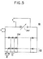
- Fig. 5 is an equivalent circuit illustrating how in the practice of the present invention a reverse voltage is applied to all the cells of a multi-cell device;
- Fig. 6 is a graphical diagram showing the trend of reverse bias current in response to increasing reverse bias voltage; and
- Figs. 7(A) through 7(D) are fragmentary, cross sectional views showing the manufacture of a further solar cell in accordance with the present invention.
- Referring to Figs. 2(A) through 2(D), a process in which pinholes are plugged with photoresist resin will first be explained.
- In the figure, a transparent electrode is formed and patterned on
transparent substrate 1 made of, for example, glass pane of 1.2 mm thick x 10 cm long x 10 cm wide. Thetransparent electrode 2 is made, inter alia, from an ITO layer 150nm (1500 angstroms) thick superimposed by aSn0₂ layer 20 to 40nm (200 to 400 angstroms) thick, an ITO layer 150nm (1500 angstroms) thick superimposed with a Sn₃N₄ layer 50nm (500 angstroms) thick, or a transparent layer doped with halogen of 150 to 200nm (1500 through 2000 angstroms) thickness mainly made of tin oxide or tin nitride by a CVD method in vacuum, a LPCVD method, a spraying method or a sputtering method. - The layers thus laminated are irradiated from upper or lower side of the
substrate 1 with laser beam of 1.06 micro meters wavelength or 0.53 micro meter wave length from a YAG laser to perform the patterning for thetransparent electrode 2. Thegrooves 13 of 10 cm long formed by the patterning partition adjacent ones of cells, each groove having 10 to 20 nm width. On the layer is formed, by a plasma or photo CVD method, anonsinglecrystal layer 3 having a p-n or p-i-n junction of 0.2 to 1.0 micro meter thickness, normally of 0.5 to 0.7 micro meter thickness. For instance, the nonsinglecrystal layer can be comprised, with a p-i-n junction, of a p-type semiconductor layer (SixC1-x; 1 >x>0) 5 to 15nm (50 to 150 angstroms) thick, an intrinsic amorphous or intrinsic semiamorphous silicon semiconductor layer 0.4 to 0.9 micro meters thick, and acrystallite layer 200 to 500 micro meters thick. - On the
semiconductor layer 3, a lot of gaps andpinholes 6 and 6' result unintentionally due to falling out of flakes which are involved into thesemiconductor layer 3 during fabrication. There are observed about two to four such defects in ten fields of view through a microscope with a magnification of 100 to 1000. - According to the described process, the
holes 6 and 6' are filled and stopped with insulator. Hereinbelow, the stopping process will be explained in detail. - The
semiconductor layer 3 with theholes 6 and 6' is coated with photocurable organic resin by a spinner or a coater in the manner that all the holes are filled completely with the resin. The organic resin may be "photoneeth" distributed from Toray Industries Inc. or other known photoresist. For instance, an amount of photoneeth having viscosity of about 120 mPa·s ( 120 CP ) is applied on thelayer 3 to 0.2 through 5.0 micrometers thickness by spinning at 500 rpm for 10 seconds and thereafter at 2000 rpm for 30 seconds followed by a prebaking at 85°C for an hour. The organic layer is irradiated withultraviolet light 17 having 300 to 400 nanometers wavelength from the glass substrate side. The ultraviolet light cannot penetrate thesemiconductor layer 3 because of the absorption in the layer whereas the resin stopping theholes 6 and 6' is cured selectively. In other words, the intensity and the wavelength are chosen so that thesemiconductor layer 3 can function as a mask. Then, the uncured resin is eliminated by a known rinsing. The remaining resin cured in the holes is chemically stabilized by sintering and post-curing. Thus the stopping process is completed. - After stopping the holes,
openings 18 are formed adjacent to thegroove 13 as shown in Fig. 2(B) by means of laser scribing to provide an access to thefirst electrodes 37 and 37'. Although theopenings 18 reach thesubstrate 1 in the figure, they can be more shallow as long as thefirst electrodes 37 and 37' are exposed from the opening. Asecond electrode 4 consisting of twoconductive layers grooves 20 by laser scribing. - The lower
conductive layer 23 may be 30 to 140nm (300 to 1400 angstroms) thick and made from ITO, In₂0₃, Sn0₂ or ITN (a mixture of indium nitride and tin nitride). The upperconductive layer 24 may be 30 to 50nm (300 to 500 angstroms) thick and made, as a single or double layer, from aluminium, chromium or silver. For example thesecond electrode 4 may be composed of an aluminium layer 100nm (1000 angstroms) thick on a ITO layer 150nm (1500 angstroms) thick. The aluminium layers 24 provide inside surfaces on which incident light entering from the substrate side can be reflected. The ITO layers 23 are disposed to prevent the aluminium layer from corroding due to interaction with the semiconductor layer. These two layers are fabricated by an electron beam deposition or a plasma CVD method at less than 300°C. As a result an improved solar cell is provided with which light having a wave length of 600 to 800 nm can be efficiently converted into electricity. - For proximate contact with a n-type semiconductor, a transparent indium compound or mixture including indium oxide and/or indium nitride is considered adequate as the
transparent layer 23. For a p-type semiconductor, a tin compound or mixture of Sn0₂, Sn₃N₄ and/or SbN is adequate in view of high efficiency and reliability for long time. - The
transparent electrode 23 is made in contact with thefirst electrode 2 at theopening 18. At this contact there is only a hetero- or homo-junction of a nitride and/or an oxide so that no interaction occurs even at 150°C, unlike the prior art illustrated in Fig.1 forming metal junction. In addition to this, such alaminated electrode 4 is advantageous especially for laser patterning. Namely thealuminium electrode 24 can be removed in the patterning together at one time with the laser scribing of thetransparent electrode 23 which is easily sublimated under irradiation of laser beam and carries the aluminium electrode thereon away from the substrate. - A passivation film of
silicon nitride 21 is deposited to 50 to 200nm (500 to 2000 angstroms) thickness by a photo CVD method or plasma vapor deposition, and a take-outline 5 is provided on thealuminium electrode 24. Thus, following placing anorganic resin layer 22 such as of polyimide, polyamide, kapton(R) or epoxy, the semiconductor device is made into a photoelectric conversion device in which a plurality ofcells connection 12. - The organic resin is provided mainly for fixation of the take-out
electrode 5. Further a device of 120 cm x 40 cm, two devices of 60 cm x 40 cm, or six devices of 40 cm x 20 cm are integrally packaged into a 120 cm x 40 cm panel according to NEDO standard. - Experimental results were obtained with a solar cell manufactured according to the above explained process having a substrate of 10 cm long x 10 cm wide as below;
open-circuit voltage 12.77 V fill factor 0.574 short-circuit current 69.0 mA conversion efficiency 7.46 % - Also, experimental results were obtained with a solar cell which was manufactured without the stopping process, but with other process steps being similar to the above, as below;
sample 1,sample 2open-circuit voltage 11.49 V 3.02 V fill factor 0.471 0.316 short-circuit current 53.7 mA 54.20 mA conversion efficiency 4.43 % 0.75 % - From the above data, it is understood that the stopping hole process makes solar cells more efficient.
- Fig. 3 shows the trend of normalized efficiencies with time passing obtained by reliability trials of solar cells manufactured with and without the hole stopping process under an atmospheric condition but at 150°
C. A curve 25 shows the normalized efficiency of a prior art solar cell having the configuration of Fig. 1; the efficiency is degraded with time passing. In the prior art device, thealuminium electrode 4 is made in contact with thesemiconductor layer 3 and in thecontact 12 there is thetin oxide layer 37 in contact with thealuminium electrode 4. These contacts give rise to oxidation of thealuminium electrode 4 and to interaction between theelectrode 4 and thesemiconductor layer 3 of n-type. Because of this, the efficiency is degraded to less than 50 % of the initial value only after ten hours or the like. - On the other hand, a
curve 26 is plotted for a solar cell made by the process of Figs 2(A) to 2(D) with resin stopping the holes and with thelaminated electrode 4. In this configuration only oxide-oxide contacts appear making thecontact 12 stable and reliable. The other important feature not illustrated in the figure is that high yield can be obtained since fluctuation of the characteristics among products is small. For instance, 0.27 was obtained as a variance of efficiency from ten samples of 10 cm long x 10 cm wide. - Referring to Figs. 4(A) to 4(D), an embodiment of the invention is illustrated. On a
substrate 1 such as a glass pane of 1.2 mm thick x 10 cm long x 10 cm wide is formed a conductivetransparent film 2, e.g., a laminated film of an ITO layer 150nm (1500 angstroms) thick on aSn0₂ layer 20 to 40nm (200 to 400 angstroms) thick or a transparent film mainly composed of tin oxide or tin nitride doped with halogen. The film may be fabricated by a LPCVD method, a plasma CVD method, a spraying method, sputtering method and an ECR method. - The
conductive film 2 is divided into a plurality of sections by patternedgrooves 13 which are formed by laser beam of 1.06 micro meters wave length or 0.53 micro meters wave length from a YAG laser controlled by a micro computer. - The patterned grooves are 50 micro meter wide and 10 cm long by which each section is partitioned from others with 10 to 20 mm width. On this film a nonmonocrystal layer is formed with a p-n junction or p-i-n junction at 0.2 to 1.0 micro meter thickness, more preferably 0.5 to 0.7 micro meter thickness. A preferred example is a laminated layer composed of a p-type semiconductor layer ( SixC1-x; 1>x>0 ) of 5 to 15nm (50 to 150 angstroms) thick, an intrinsic amorphous or intrinsic semiamorphous silicon semiconductor layer 0.4 to 0.9 micro meter thick, and a
crystal layer 200 to 500 micro meter thick. - The
semiconductor layer 3 with theholes 6 and 6' is coated with photocurable organic resin in the manner that all the holes are filled completely with the resin by a spinner or a coater. The organic resin may be a photoresist of positive type such as OFPR-800 distributed by Tokyo Ohka Kogyo Co., Ltd. or other known photo resist. For instance, an amount of photoresist is applied on thelayer 3 to a thickness of 0.1 through 5.0 micro meters by spinning at 500 rpm for 5 seconds and thereafter at 2000 rpm for an appropriate period followed by a prebaking at 85°C for 40 minutes. Theorganic layer 3 is irradiated withultraviolet light 17 having 300 to 400 nanometers wavelength from the resist side. As the curing for OFPR-800, irradiation of ultraviolet light of 6 mW/cm² for 5 seconds is carried out, followed by aftertreatments. Then, the uncured resin is eliminated by a known rinsing with pure water for 10 minutes. The remaining resin cured in the holes is chemically stabilized by sinter and post-cure. For instance, the layer is let undergo post baking for an hour at 150°C. Thus the stopping process is completed. - After stopping the holes,
openings 18 are formed adjacent to thegroove 13 as shown in Fig. 4(B) by means of laser scribing to provide an access to thefirst electrodes 37 and 37'. Although theopenings 18 reach thesubstrate 1 in the figure, they can be more shallow as long as thefirst electrodes 37 and 37' are accessed. Asecond electrode 4 consisting of twoconductive layers grooves 20 scribed by laser scribing. - The second electrode may be a transparent
conductive layer 30 to 50nm (300 to 500 angstroms) thick, for example, made of ITO, In₂0₃ Sn0₂ or ZnO through which incident light can go out of the device. - On the other hand, the second electrode may be formed reflective by deposition, on the transparent electrode, of aluminium, chromium or silver as a single-layered reflective film, or aluminium and nickel as a double-layered reflective film. In this embodiment, the second electrode is comprised of an ITO layer 105nm (1050 angstroms) thick and an aluminium layer 100nm (1000 angstroms) thick. The electrode can be formed by sputtering, an electron beam deposition or plasma CVD method at less than 300°C in order not to render the semiconductor degraded.
- Referring to Fig. 4(D) and Fig. 5, a reverse bias applying circuit is illustrated. The circuit comprises a
power supply 240 and a number ofZener diodes 230. Between each adjacent ones of thediodes 23 and between the power supply and the first or last diodes are made contact with the first and second electrodes respectively so that the output voltage is divided into the reverse bias voltage which is applied to each of the cells constituting the device. The reverse bias voltage must be less than the breakdown voltage of the p-i-n junction of thesemiconductor layer 3. Because of this the reverse bias voltage does not cause current to pass through flawless portions of thesemiconductor layer 2. To preclude breakdown of the p-i-n junction further, the zener diodes are selected out of a variety of voltage dividing element candidates. The zener voltage is chosen slightly below the breakdown voltage of the p-i-n junction. - In Fig. 5, the circuit diagram includes the number of the cells constituting the device each of which is represented by a diode corresponding to the
semiconductor layer 2 and a resistance corresponding to the defects (holes) as leakage source. TheZener diode 230 is connected in parallel to the diode and the resistance so that the voltage applied to thediode 25 is kept below the breakdown voltage thereof. - With the bias voltage less than the breakdown voltage, the holes or flaws in the
semiconductor layer 3 filled with the organic resin become current passages which are heated as electric current flows therethrough. The electric power is sometimes short of burning out the holes or flaws completely. To make the burning out easy, thesubstrate 1 is heated in advance together with the semiconductor to less than the temperature at which the semiconductor may be degraded, normally less than 150°C. - An experiment was made with a device having 15 cells connected with each other and the bias voltage was chosen at 120 V. As a result, the current trend in response to increasing reverse bias voltage was obtained as shown in Fig.6.
- In the experiment, the reverse bias voltage increased from 0 V to 120 V. A first leakage current was observed at 30-1. However the leakage current was cured because of burning out due to the concentrated current flow. As the reverse bias voltage increased, a number of current ripples were observed. The magnitude of the leakage current became larger at the higher reverse bias voltage. With the reverse bias voltage decreasing from a
point 32, the reverse bias current smoothly dropped without leakage current. - For reference, the device thus treated was subjected to increasing reverse bias voltage. No leakage current, however, was observed until reverse current was raised at the withstand voltage.
- After removing the bias applying circuit, the device integrated on a 10 cm x 10 cm panel was irradiated with light of 100 mW/cm2 (AM1). The characteristics obtained are;
open-circuit voltage 12.943 V fill factor 0.6641 short-circuit current 79.34 mA current density 17.290 mA/cm² efficiency 9.90 % - With the device fabricated according to a process identical to that of Fig. 4 but without reverse bias curing, the following
experimental data 1 were obtained, and without stopping process and reverse bias curing, the followingexperimental data 2 were obtained:data 1data 2open-circuit voltage 12.315 V 11.49 V fill factor 0.597 0.471 short-circuit current 79.34 mA 53.7 mA efficiency 8.33 % 4.43 % - Compared with the figures obtained with the initial embodiment, it is understood that the device having undergone the reverse bias voltage demonstrates further improved characteristics. The reason why the reverse bias curing is effective is considered to be that a chemical reaction between the resin and the semiconductor may produce a stable insulator tightly joined to the pin-holes.
- A further embodiment of the invention is shown in Fig. 7. In this embodiment, the process is similar to that of the preceding embodiment. So only different configurations are described and redundant explanation is not repeated.
- A
substrate 1 is composed of a conductivestainless foil 40 of 10 to 100 micro meters thickness and a heatproof organic resin film or an inorganic insulator film such as made ofenamel 41 on thestainless foil 40. On thesubstrate 1, afirst electrode 2 is formed, for example, made of a 20nm (200 angstroms) thick chromium layer, a 150nm (1500 angstroms) thick aluminium layer plus a 50nm (500 angstroms) thick Sn₃N₄ layer or a 150 to 200nm (1500 to 2000 angstroms) thick transparent conductive layer mainly composed of tin oxide or tin nitride doped with halogen. -
Grooves 8 which provide accesses to the first electrode reach only to the surface of thefirst electrode 2 at which the second electrode can be in contact with thefirst electrode 2. - After removing the bias applying circuit, the device integrated on a 10 cm x 10 cm panel was irradiated with light of 100 mW/cm² (AM1). The characteristics obtained are;
open-circuit voltage 12.618 V fill factor 0.678 short-circuit current 79.710 mA current density 17.371 mA/cm² efficiency 9.82 % - With the device fabricated according to the process identical to that in Fig. 7 but without reverse bias curing, the following
experimental data 1 were obtained, and without both stopping process and reverse bias curing, the followingexperimental data 2 were obtained:data 1data 2open-circuit voltage 11.30 V 6.54 V fill factor 0.626 0.368 short-circuit current 79.4 mA 75.69 mA efficiency 8.16 % 3.48 % - The other important feature is that high yield can be obtained since the fluctuation of the characteristics is small among products. For instance, 0.195 (X 9.63%) was obtained as a variance of efficiency from ten samples of 10 cm long x 10 cm wide prepared according to NEDO standard.
- Examples of variations which can be made are as follow.
- The semiconductor layer may be constituted with multijunction structure in place of single junction structure. Namely, the layer can be a laminate composed of a p-type semiconductor (SixC1-x), an intrinsic amorphous silicon semiconductor, an n-type silicon semiconductor, a p-type semiconductor (SixC1-x), an intrinsic semiconductor (SixGe1-x) and n-type
silicon semiconductor layer 30 to 100nm (300 to 1000 angstroms) thick, wherein 0 < X < 1, e.g., X = 0.5. - To engrave the grooves, one line of the grooves can be formed at once by irradiating with laser beam extending in lateral direction which is produced from an excimer laser through a cylindrical lens, if necessary, after expansion of original beam.
- The above technique according to the invention is applicable also to a light emitting semiconductor device with double heterojunctions and a superlattice structure. As such devices, the applicant has disclosed some semiconductor devices in US-A-4,527,179 and US-A-4,616,244.
- The invention is advantageous also when applied to a diode array of an image sensor or a nonlinear element of a thin film display. In some applications, the reverse bias voltage circuit can be much simplified. For example, an active device can be cured by applying a reverse voltage to source, drain and/or gate electrodes.
Claims (13)
- A method of manufacturing a semiconductor device in which a semiconductor layer is sandwiched between first and second electrode layers, said method including the filling of pinholes and other gaps in the semiconductor layer with an insulating resin material before the formation of the second electrode, and being characterized in that the second electrode layer comprises a conductive transparent compound or mixture, and further characterised by the application after the second electrode is formed of a reverse voltage less than the breakdown voltage of the semiconductor layer between the first and second electrodes in order to eliminate shorts and shunts of the semiconductor layer.
- A method as claimed in claim 1 wherein the insulating resin material is a photocurable resin and the method includes the application of the photocurable resin to a surface of the semiconductor layer, the subsequent irradiation of the photocurable resin with the semiconductor layer serving as a mask so as to cure the resin filling the pinholes and other gaps in the semiconductor layer, and the removal of uncured resin from the semiconductor layer.
- A method as claimed in claim 1 or 2 wherein the application of the reverse voltage between the first and second electrodes is effected with the semiconductor layer heated to an elevated temperature selected so as not to risk degradation of the characteristics of the semiconductor layer.
- A method as claimed in any of the preceding claims wherein the semiconductor device comprises a plurality of series connected solar cells each comprising a respective semiconductor layer and respective first and second electrodes, and the application of a reverse voltage to each of said cells is effected by use of a voltage source and a plurality of series connected Zener diodes which are coupled to the series connected solar cells so that each cell has applied thereto a reverse voltage determined by a respective one of the Zener diodes and less than the breakdown voltage of the cell.
- A method as claimed in any of the preceding claims wherein said semiconductor junction layer is an amorphous semiconductor layer incorporating a p-i-n junction.
- A method as claimed in any of the preceding claims wherein said semiconductor device comprises a photovoltaic device.
- A method as claimed in any of claims 1 to 5 wherein said semiconductor device comprises a light emitting device.
- A method as claimed in claim 7 wherein said light emitting device has a superlattice structure.
- A method according to any preceding claim wherein said substrate is glass.
- A method according to any preceding claim wherein said first electrode comprises a transparent conductive material.
- A method according to any preceding claim, wherein said second electrode comprises a metal layer formed over said conductive transparent compound or mixture.
- A method according to claim 11 wherein said metal is aluminium, silver or chromium.
- A method according to any preceding, claim in which said conductive transparent compound or mixture comprises ITO, In₂O₃ or SnO₂.
Applications Claiming Priority (6)
| Application Number | Priority Date | Filing Date | Title |
|---|---|---|---|
| JP60186206A JPS6254479A (en) | 1985-08-24 | 1985-08-24 | Preparation for photoelectric conversion device |
| JP60186205A JPS6254478A (en) | 1985-08-24 | 1985-08-24 | Optoelectric transducer |
| JP186205/85 | 1985-08-24 | ||
| JP186206/85 | 1985-08-24 | ||
| JP248640/85 | 1985-11-06 | ||
| JP60248640A JPH0620148B2 (en) | 1985-11-06 | 1985-11-06 | Semiconductor device manufacturing method |
Publications (3)
| Publication Number | Publication Date |
|---|---|
| EP0213910A2 EP0213910A2 (en) | 1987-03-11 |
| EP0213910A3 EP0213910A3 (en) | 1988-10-05 |
| EP0213910B1 true EP0213910B1 (en) | 1994-03-02 |
Family
ID=27325704
Family Applications (1)
| Application Number | Title | Priority Date | Filing Date |
|---|---|---|---|
| EP86306556A Expired - Lifetime EP0213910B1 (en) | 1985-08-24 | 1986-08-22 | Method of manufacturing a semiconductor device free from the current leakage through a semi-conductor layer |
Country Status (4)
| Country | Link |
|---|---|
| US (2) | US4937651A (en) |
| EP (1) | EP0213910B1 (en) |
| AU (1) | AU594359B2 (en) |
| DE (1) | DE3689679T2 (en) |
Families Citing this family (38)
| Publication number | Priority date | Publication date | Assignee | Title |
|---|---|---|---|---|
| AU583423B2 (en) * | 1985-09-21 | 1989-04-27 | Semiconductor Energy Laboratory Co. Ltd. | Semiconductor device free from the electrical shortage through a semiconductor layer and method for manufacturing same |
| US4774193A (en) * | 1986-03-11 | 1988-09-27 | Siemens Aktiengesellschaft | Method for avoiding shorts in the manufacture of layered electrical components |
| JP2680002B2 (en) * | 1987-11-14 | 1997-11-19 | キヤノン株式会社 | Photoelectric conversion device |
| US4981525A (en) * | 1988-02-19 | 1991-01-01 | Sanyo Electric Co., Ltd. | Photovoltaic device |
| US4893171A (en) * | 1988-03-30 | 1990-01-09 | Director General, Agenty Of Industrial Science And Technology | Semiconductor device with resin bonding to support structure |
| US5266828A (en) * | 1988-10-14 | 1993-11-30 | Matsushita Electric Industrial Co., Ltd. | Image sensors with an optical fiber array |
| DE68926448T2 (en) * | 1988-10-14 | 1996-12-12 | Matsushita Electric Ind Co Ltd | IMAGE SENSOR AND METHOD FOR THE PRODUCTION THEREOF |
| US5139970A (en) * | 1989-06-01 | 1992-08-18 | Semiconductor Energy Laboratory Co., Ltd. | Electric device and manufacturing method of the same |
| US5279678A (en) * | 1992-01-13 | 1994-01-18 | Photon Energy, Inc. | Photovoltaic cell with thin CS layer |
| US5501744A (en) * | 1992-01-13 | 1996-03-26 | Photon Energy, Inc. | Photovoltaic cell having a p-type polycrystalline layer with large crystals |
| US6023318A (en) * | 1996-04-15 | 2000-02-08 | Canon Kabushiki Kaisha | Electrode plate, process for producing the plate, liquid crystal device including the plate and process for producing the device |
| DE19842679C2 (en) * | 1998-09-17 | 2000-12-21 | Siemens Solar Gmbh | Process for structuring transparent electrode layers |
| US8138413B2 (en) | 2006-04-13 | 2012-03-20 | Daniel Luch | Collector grid and interconnect structures for photovoltaic arrays and modules |
| US8222513B2 (en) | 2006-04-13 | 2012-07-17 | Daniel Luch | Collector grid, electrode structures and interconnect structures for photovoltaic arrays and methods of manufacture |
| US7507903B2 (en) | 1999-03-30 | 2009-03-24 | Daniel Luch | Substrate and collector grid structures for integrated series connected photovoltaic arrays and process of manufacture of such arrays |
| US20090111206A1 (en) | 1999-03-30 | 2009-04-30 | Daniel Luch | Collector grid, electrode structures and interrconnect structures for photovoltaic arrays and methods of manufacture |
| US8664030B2 (en) | 1999-03-30 | 2014-03-04 | Daniel Luch | Collector grid and interconnect structures for photovoltaic arrays and modules |
| US7288420B1 (en) | 1999-06-04 | 2007-10-30 | Semiconductor Energy Laboratory Co., Ltd. | Method for manufacturing an electro-optical device |
| US8198696B2 (en) | 2000-02-04 | 2012-06-12 | Daniel Luch | Substrate structures for integrated series connected photovoltaic arrays and process of manufacture of such arrays |
| FR2818442B1 (en) * | 2000-12-20 | 2003-10-17 | Energy Systems Internat Bv | WINDOW-FORMING PHOTOVOLTAIC DEVICE |
| US6777249B2 (en) | 2001-06-01 | 2004-08-17 | Semiconductor Energy Laboratory Co., Ltd. | Method of repairing a light-emitting device, and method of manufacturing a light-emitting device |
| US20050212000A1 (en) * | 2004-03-26 | 2005-09-29 | Semiconductor Energy Laboratory Co., Ltd. | Method for manufacturing light emitting device, and electronic device |
| US7838868B2 (en) * | 2005-01-20 | 2010-11-23 | Nanosolar, Inc. | Optoelectronic architecture having compound conducting substrate |
| US7732229B2 (en) * | 2004-09-18 | 2010-06-08 | Nanosolar, Inc. | Formation of solar cells with conductive barrier layers and foil substrates |
| US7276724B2 (en) * | 2005-01-20 | 2007-10-02 | Nanosolar, Inc. | Series interconnected optoelectronic device module assembly |
| US8927315B1 (en) | 2005-01-20 | 2015-01-06 | Aeris Capital Sustainable Ip Ltd. | High-throughput assembly of series interconnected solar cells |
| US9236512B2 (en) | 2006-04-13 | 2016-01-12 | Daniel Luch | Collector grid and interconnect structures for photovoltaic arrays and modules |
| US8729385B2 (en) | 2006-04-13 | 2014-05-20 | Daniel Luch | Collector grid and interconnect structures for photovoltaic arrays and modules |
| US8884155B2 (en) | 2006-04-13 | 2014-11-11 | Daniel Luch | Collector grid and interconnect structures for photovoltaic arrays and modules |
| US9006563B2 (en) | 2006-04-13 | 2015-04-14 | Solannex, Inc. | Collector grid and interconnect structures for photovoltaic arrays and modules |
| US8822810B2 (en) | 2006-04-13 | 2014-09-02 | Daniel Luch | Collector grid and interconnect structures for photovoltaic arrays and modules |
| US9865758B2 (en) | 2006-04-13 | 2018-01-09 | Daniel Luch | Collector grid and interconnect structures for photovoltaic arrays and modules |
| EP2161760B1 (en) * | 2008-09-05 | 2017-04-12 | Semiconductor Energy Laboratory Co., Ltd. | Photoelectric Conversion Device |
| US8247243B2 (en) | 2009-05-22 | 2012-08-21 | Nanosolar, Inc. | Solar cell interconnection |
| US9059347B2 (en) | 2010-06-18 | 2015-06-16 | Semiconductor Energy Laboratory Co., Ltd. | Photoelectric conversion device and manufacturing method thereof |
| JP2012064933A (en) | 2010-08-19 | 2012-03-29 | Semiconductor Energy Lab Co Ltd | Photoelectric conversion module and its manufacturing method |
| US8557614B2 (en) | 2010-12-28 | 2013-10-15 | Semiconductor Energy Laboratory Co., Ltd. | Method for manufacturing lighting device |
| WO2012103655A1 (en) * | 2011-02-04 | 2012-08-09 | Von Roll Solar Ag | Method for filling defects in a photovoltaic apparatus |
Family Cites Families (21)
| Publication number | Priority date | Publication date | Assignee | Title |
|---|---|---|---|---|
| US3946278A (en) * | 1973-12-19 | 1976-03-23 | Westinghouse Air Brake Company | Fail-safe four leaded zener diode arrangement |
| US4166918A (en) * | 1978-07-19 | 1979-09-04 | Rca Corporation | Method of removing the effects of electrical shorts and shunts created during the fabrication process of a solar cell |
| JPS5613778A (en) | 1979-07-16 | 1981-02-10 | Shunpei Yamazaki | Photoelectric converter and its preparation |
| JPS5613777A (en) | 1979-07-16 | 1981-02-10 | Shunpei Yamazaki | Photoelectric converter |
| JPS5613779A (en) | 1979-07-16 | 1981-02-10 | Shunpei Yamazaki | Photoelectric converter and its preparation |
| JPS55124274A (en) | 1980-02-04 | 1980-09-25 | Sanyo Electric Co Ltd | Solar battery |
| US4292092A (en) * | 1980-06-02 | 1981-09-29 | Rca Corporation | Laser processing technique for fabricating series-connected and tandem junction series-connected solar cells into a solar battery |
| DE3047383A1 (en) * | 1980-12-16 | 1982-07-15 | Siemens AG, 1000 Berlin und 8000 München | SOLAR CELL WITH INCREASED EFFICIENCY |
| JPS57117276A (en) * | 1981-01-14 | 1982-07-21 | Hitachi Ltd | Semiconductor device |
| US4527179A (en) * | 1981-02-09 | 1985-07-02 | Semiconductor Energy Laboratory Co., Ltd. | Non-single-crystal light emitting semiconductor device |
| CA1165016A (en) * | 1981-03-16 | 1984-04-03 | Bulent M. Basol | Plugged pinhole thin film and method of making same |
| US4420497A (en) * | 1981-08-24 | 1983-12-13 | Fairchild Camera And Instrument Corporation | Method of detecting and repairing latent defects in a semiconductor dielectric layer |
| JPS5877263A (en) * | 1981-11-02 | 1983-05-10 | Agency Of Ind Science & Technol | Photoelectromotive force element |
| US4640002A (en) * | 1982-02-25 | 1987-02-03 | The University Of Delaware | Method and apparatus for increasing the durability and yield of thin film photovoltaic devices |
| JPS5935490A (en) * | 1982-08-24 | 1984-02-27 | Sanyo Electric Co Ltd | Manufacture of photo semiconductor device |
| DE3312053C2 (en) * | 1983-04-02 | 1985-03-28 | Nukem Gmbh, 6450 Hanau | Method for preventing short circuits or shunts in a large-area thin-film solar cell |
| AU2042183A (en) * | 1983-08-03 | 1985-02-07 | Energy Conversion Devices Inc. | Eliminating short circuits in photovoltaic devices |
| JPS6050979A (en) | 1983-08-30 | 1985-03-22 | Semiconductor Energy Lab Co Ltd | Light emitting semiconductor device |
| US4633034A (en) * | 1985-02-08 | 1986-12-30 | Energy Conversion Devices, Inc. | Photovoltaic device and method |
| US4698494A (en) * | 1985-06-06 | 1987-10-06 | Fuji Electric Co., Ltd. | Image sensor and method of making |
| JPS6258685A (en) * | 1985-09-09 | 1987-03-14 | Fuji Electric Co Ltd | Manufacture of amorphous semiconductor solar cell |
-
1986
- 1986-08-22 AU AU61781/86A patent/AU594359B2/en not_active Ceased
- 1986-08-22 US US06/899,160 patent/US4937651A/en not_active Expired - Lifetime
- 1986-08-22 EP EP86306556A patent/EP0213910B1/en not_active Expired - Lifetime
- 1986-08-22 DE DE3689679T patent/DE3689679T2/en not_active Expired - Fee Related
-
1987
- 1987-09-04 US US07/092,943 patent/US4786607A/en not_active Expired - Lifetime
Non-Patent Citations (1)
| Title |
|---|
| The New Penguin Dictionary of Electronics, ed. Valerie Pitt, page 378. * |
Also Published As
| Publication number | Publication date |
|---|---|
| AU594359B2 (en) | 1990-03-08 |
| DE3689679T2 (en) | 1994-06-09 |
| US4786607A (en) | 1988-11-22 |
| AU6178186A (en) | 1987-02-26 |
| US4937651A (en) | 1990-06-26 |
| EP0213910A2 (en) | 1987-03-11 |
| EP0213910A3 (en) | 1988-10-05 |
| DE3689679D1 (en) | 1994-04-07 |
Similar Documents
| Publication | Publication Date | Title |
|---|---|---|
| EP0213910B1 (en) | Method of manufacturing a semiconductor device free from the current leakage through a semi-conductor layer | |
| US5089426A (en) | Method for manufacturing a semiconductor device free from electrical shortage due to pin-hole formation | |
| US4725558A (en) | Semiconductor defects curing method and apparatus | |
| US5133809A (en) | Photovoltaic device and process for manufacturing the same | |
| US4292092A (en) | Laser processing technique for fabricating series-connected and tandem junction series-connected solar cells into a solar battery | |
| US4428110A (en) | Method of making an array of series connected solar cells on a single substrate | |
| US4443651A (en) | Series connected solar cells on a single substrate | |
| US4517403A (en) | Series connected solar cells and method of formation | |
| US4640002A (en) | Method and apparatus for increasing the durability and yield of thin film photovoltaic devices | |
| US4824488A (en) | Photovoltaic device | |
| US7547570B2 (en) | Method for forming thin film photovoltaic interconnects using self-aligned process | |
| US4084985A (en) | Method for producing solar energy panels by automation | |
| US4689874A (en) | Process for fabricating a thin-film solar battery | |
| JP2986875B2 (en) | Integrated solar cell | |
| US20140174530A1 (en) | Solar cell and manufacturing method thereof | |
| US5164322A (en) | Method for manufacturing photoelectric conversion device with a high response speed | |
| JPH0851229A (en) | Integrated solar battery and its manufacture | |
| JPH06318723A (en) | Photovoltaic element and its manufacture | |
| EP0087776B1 (en) | Method and apparatus for increasing the durability and yield of thin film photovoltaic devices | |
| JPH0419713B2 (en) | ||
| JPH0558585B2 (en) | ||
| JPS6254478A (en) | Optoelectric transducer | |
| JP2883370B2 (en) | Photovoltaic device | |
| JPH0620148B2 (en) | Semiconductor device manufacturing method | |
| JPS6254479A (en) | Preparation for photoelectric conversion device |
Legal Events
| Date | Code | Title | Description |
|---|---|---|---|
| PUAI | Public reference made under article 153(3) epc to a published international application that has entered the european phase |
Free format text: ORIGINAL CODE: 0009012 |
|
| AK | Designated contracting states |
Kind code of ref document: A2 Designated state(s): DE FR GB |
|
| RAP1 | Party data changed (applicant data changed or rights of an application transferred) |
Owner name: SEMICONDUCTOR ENERGY LABORATORY CO., LTD. |
|
| PUAL | Search report despatched |
Free format text: ORIGINAL CODE: 0009013 |
|
| AK | Designated contracting states |
Kind code of ref document: A3 Designated state(s): DE FR GB |
|
| 17P | Request for examination filed |
Effective date: 19881223 |
|
| 17Q | First examination report despatched |
Effective date: 19910212 |
|
| GRAA | (expected) grant |
Free format text: ORIGINAL CODE: 0009210 |
|
| AK | Designated contracting states |
Kind code of ref document: B1 Designated state(s): DE FR GB |
|
| REF | Corresponds to: |
Ref document number: 3689679 Country of ref document: DE Date of ref document: 19940407 |
|
| ET | Fr: translation filed | ||
| PLBE | No opposition filed within time limit |
Free format text: ORIGINAL CODE: 0009261 |
|
| STAA | Information on the status of an ep patent application or granted ep patent |
Free format text: STATUS: NO OPPOSITION FILED WITHIN TIME LIMIT |
|
| 26N | No opposition filed | ||
| REG | Reference to a national code |
Ref country code: GB Ref legal event code: IF02 |
|
| PGFP | Annual fee paid to national office [announced via postgrant information from national office to epo] |
Ref country code: FR Payment date: 20030808 Year of fee payment: 18 |
|
| PGFP | Annual fee paid to national office [announced via postgrant information from national office to epo] |
Ref country code: GB Payment date: 20030820 Year of fee payment: 18 |
|
| PGFP | Annual fee paid to national office [announced via postgrant information from national office to epo] |
Ref country code: DE Payment date: 20030904 Year of fee payment: 18 |
|
| PG25 | Lapsed in a contracting state [announced via postgrant information from national office to epo] |
Ref country code: GB Free format text: LAPSE BECAUSE OF NON-PAYMENT OF DUE FEES Effective date: 20040822 |
|
| PG25 | Lapsed in a contracting state [announced via postgrant information from national office to epo] |
Ref country code: DE Free format text: LAPSE BECAUSE OF NON-PAYMENT OF DUE FEES Effective date: 20050301 |
|
| GBPC | Gb: european patent ceased through non-payment of renewal fee |
Effective date: 20040822 |
|
| PG25 | Lapsed in a contracting state [announced via postgrant information from national office to epo] |
Ref country code: FR Free format text: LAPSE BECAUSE OF NON-PAYMENT OF DUE FEES Effective date: 20050429 |
|
| REG | Reference to a national code |
Ref country code: FR Ref legal event code: ST |