EP0213687A2 - A thin film magnetic transducer - Google Patents
A thin film magnetic transducer Download PDFInfo
- Publication number
- EP0213687A2 EP0213687A2 EP86303214A EP86303214A EP0213687A2 EP 0213687 A2 EP0213687 A2 EP 0213687A2 EP 86303214 A EP86303214 A EP 86303214A EP 86303214 A EP86303214 A EP 86303214A EP 0213687 A2 EP0213687 A2 EP 0213687A2
- Authority
- EP
- European Patent Office
- Prior art keywords
- winding
- transducer
- turns
- windings
- magnetic
- Prior art date
- Legal status (The legal status is an assumption and is not a legal conclusion. Google has not performed a legal analysis and makes no representation as to the accuracy of the status listed.)
- Granted
Links
Images


Classifications
-
- G—PHYSICS
- G11—INFORMATION STORAGE
- G11B—INFORMATION STORAGE BASED ON RELATIVE MOVEMENT BETWEEN RECORD CARRIER AND TRANSDUCER
- G11B5/00—Recording by magnetisation or demagnetisation of a record carrier; Reproducing by magnetic means; Record carriers therefor
- G11B5/127—Structure or manufacture of heads, e.g. inductive
- G11B5/31—Structure or manufacture of heads, e.g. inductive using thin films
- G11B5/3109—Details
- G11B5/313—Disposition of layers
-
- G—PHYSICS
- G11—INFORMATION STORAGE
- G11B—INFORMATION STORAGE BASED ON RELATIVE MOVEMENT BETWEEN RECORD CARRIER AND TRANSDUCER
- G11B5/00—Recording by magnetisation or demagnetisation of a record carrier; Reproducing by magnetic means; Record carriers therefor
- G11B5/127—Structure or manufacture of heads, e.g. inductive
- G11B5/31—Structure or manufacture of heads, e.g. inductive using thin films
- G11B5/3109—Details
- G11B5/312—Details for reducing flux leakage between the electrical coil layers and the magnetic cores or poles or between the magnetic cores or poles
- G11B5/3123—Details for reducing flux leakage between the electrical coil layers and the magnetic cores or poles or between the magnetic cores or poles by using special coil configurations or conductors
Definitions
- This invention relates to a thin film magnetic transducer for reading and writing digital data on a magnetic disc.
- the need for increased data density has led to a reduction in the track width for recording and reading data, thereby reducing the magnitude of signals from the transducer.
- An additional requirement of thinner magnetic disc media for high density memory applications will tend to still further reduce the magnitude of these signals. It is also advantageous to have the transducer write efficiently with relatively low write currents.
- One way of generating additional signal amplitude and writing with low current is to add additional turns to the winding disposed between the pole pieces of a thin film transducer.
- the addition of more windings has limitations.
- the transducer efficiency is controlled, in part, by the length of the region between the pole piece back gap region and pole tip region. As the distance between these two regions increases to make room for additional winding turns, a decrease in efficiency occurs.
- US-A-4 318 148 discloses a thin film magnetic transducer including lower and upper magnetic layers forming a magnetic circuit loop containing a transducing gap and a back gap closure, the upper magnetic layer having end portions which slope down towards the lower magnetic layer adjacent the transducing gap and adjacent the back gap closure, lower and upper planar multi-turn conductive windings which are parallel, insulated from one another and from the magnetic layers, and with each turn passing through the magnetic circuit loop.
- a transducer having the features specified in the foregoing paragraph is characterised according to the invention, by the distance from the outside of the outermost turn to the outside of the innermost turn of the portion of the upper winding passing through the magnetic circuit loop being slightly less than the distance from the outside of the outermost turn to the outside of the innermost turn of the portion of the lower winding passing through the magnetic circuit loop so that the innermost and the outermost turns of the upper winding are well insulated from the sloping end portions of the upper magnetic layer.
- a centre tapped structure be provided which will permit half the turns to be used during a writing sequence, and to use all the turns in a sensing mode during a data read operation.
- writing should be possible using either half of the winding in a centre tapped structure, without a different drive circuit for each winding half.
- each winding half of a centre tapped structure should have the equivalent impedance, in both inductive and resistive components.
- each winding has the same number of turns and is joined at a common connection providing a centre tapped winding.
- the centre to centre spacing of the turns of the second winding is slightly different from the centre to centre spacing of the turns of the first winding.
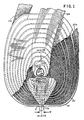
- a thin film magnetic transducer has a pole tip region P which abuts against an air bearing surface for reading and writing digital data on a magnetic disc carrier.
- the pole tip region P provides a magnetic transducing gap defined by a non-magnetic spacing 13 which may be an insulating material such as aluminium oxide.
- a non-magnetic spacing 13 which may be an insulating material such as aluminium oxide.
- a first magnetic pole piece 12 On one side of the non-magnetic spacing 13 is a first magnetic pole piece 12 and on the other side a second magnetic pole piece 11.
- these various layers are deposited on a substrate 10, the substrate 10 generally holding a plurality of such thin film transducers made through deposition processes.
- the first pole piece 12 is deposited on substrate 10.
- the pole piece In the pole tip region P, the pole piece is seen to have a width of W which is slightly less than or equal to the width of a track of the magnetic disc carrier.
- the pole piece 12, generally comprising a layer of nickel-iron NiFe material extends rearwards and beyond the pole tip region, diverging laterally at an angle ⁇ .
- a back gap closure 19 is positioned at the rearmost portion of the pole piece 12 which completes the magnetic circuit for pole pieces 11 and 12.
- the transducer gap non-magnetic material 13 is next deposited over the entire surface of the pole piece 12 when the material 13 is an insulator, in that region between the air bearing transducing surface and the back gap closure 19 region of the thin film transducer. However, the extent of material 13 must be more closely controlled when the material 13 is conductive, to avoid shorting the turns of the winding to be described below.
- This layer 15 supports a plurality of segments of a single, continuous winding 17.
- the insulation layer 15 has in the pole tip region a generally sloping termination portion, the front edge of which defines one end of the transducer throat height. The remaining end of the throat height is defined by the ABS air bearing surface at the end of the pole piece.
- the winding 17, the first of two windings comprises in the preferred embodiment, twelve turns which begin at an exterior connection point 17a, and continue spirally wound counter clockwise on the insulation layer 15 to a centrally located connection point 17b.
- the winding turns 17 which traverse the region between the pole tip and magnetic back closure area are shown to be generally transverse to the axis of the pole piece ends.
- the turns or segments of winding 17 between pole pieces 11 and 12 are equally spaced, having a centre line to centre line spacing of D2. Additionally, each edge of the exterior segments of winding 17 in the pole tip region is spaced away from the remaining pole piece 11.
- the winding 17 can be formed by depositing an electrically conductive material such as copper.
- the insulation layer 18 forms a support basis for yet another twelve turn spiral winding 20 having a centrally located winding end 20b positioned over the winding end 17b, see Figure 2B.
- winding 20 includes a plurality of spiral clockwise segments having a centre line to centre line spacing D1 smaller than the first winding 17. Additionally, there is a corresponding reduction in the width W1 of each conductor of the second winding compared with the width W2 of each conductor of the first winding.
- the winding 20 may also be made of copper or any other suitable electrically conductive material.
- the resulting pair of windings 17 and 20 each have correspondingly deposited first end connection portions 20a and 17a which are accessible at the edge of the substrate 10.
- a final deposition process step deposits a layer 11 of NiFe material which forms the remaining pole piece for the magnetic thin film transducer.
- the second pole piece 11 includes first and second transition regions 11a and 11b at the pole piece tip region, and similar transition regions 11d and 11e at the back gap region which traverse the multiple layers of insulation and conductor windings formed in the thin film transducer.
- the addition of only a single twelve turn winding provides for a sloping geometry for this transition region which does not create high risks of shorting the end turns of windings 17 and 20 with the deposited pole piece transition regions 11a, 11b, 11d and 11e.
- the back portion of the transducer winding conductor segments which join with the conductor segments 17 and 20 in the pole tip region are shown more particularly in Figure 2B.
- Rearward of the back gap closure 19 is shown a centre tap connection which includes conductor ends 20b and 17b and conductor 24.
- Conductor 24 is generally deposited at the same time as pole piece 11 and therefore is made of NiFe which is also an electrically conductive material.
- These individual conductor seg ments of windings 17 and 20 outside of the pole tip region are shown having a common spacing and width since the inductance of the winding is determined principally by those conductor segments of the windings in the pole tip region.
- Winding end 20b includes an integral foot member 20c which is deposited through a mask to contact winding end 27b.
- Conductor 24 also is shown having an integral foot member 24b contacting winding end 20b.
- conductor 24 provides a centre tap connection to the ends of windings 17 and 20. Insulation layers 15, 18 and 21 are deposited at the same time the corresponding insulation layers in the pole tip region are deposited to maintain the windings from contacting each other beyond the centre tap connection.
- the windings 17 and 20 provide a continuous single direction current path.
- the magnetic transitions on the disc are sensed by the pole pieces 11 and 12 which induce a voltage across the windings 17 and 20. This voltage can be measured at the winding ends 17a and 20a.
- the windings 17 and 20 are wound in the same sense, that is, as shown in Figure 2A, the conductor coil starts at the winding end 20a, proceeds in a clockwise spiral direction through winding 20 around the back gap closure 19, ends the spiral at the conductor end 20b and continues through the integral foot member 20c into the conductor end 17b into the winding 17 which proceeds in a clockwise expanding spiral direction to the winding end 17a.
- the direction of the winding is arbitrary and can be considered to be counterclockwise if the direction starts at the winding end 17a with either the winding 20 being deposited on top of the winding 17 or the winding 20 being deposited on top of the winding 17 or the winding 17 being deposited on top of the winding 20.
- the windings 17 and 20 are wound in the same sense so that the voltage induced in each are added to produce the total output voltage, and not subtracted which would effectively cancel the outputs.
- the centre line to centre line spacing of 2 of the turns of winding 17 is selected to be approximately 8 microns, and the centre line to centre line spacing D1 of the coil member 20 is selected to be approximately 7.5 microns.
- the effect of the narrower spacing for conductor winding 20 is to draw the conductor 20' nearest the air bearing surface and nearest the back gap closure inward approximately 3 microns, relative to the corresponding first layer turns of winding 17. This spaces the conductor 20' nearest the air bearing surface and the back gap closure the same distance from region 11a and 11d, as the corresponding conductors of winding 17.
- the inductance associated with each turn of each winding is determined only by the distance of the turn from the back gap closure.
- the resistance of each of the two windings can be maintained by plating thickness control during the deposition of each winding.
- An additional advantage of the two-winding structure is that a differential read circuit can be employed, where the two windings are serially connected, using the centre tap as a common connection, and differential measurements of flux change are made when data is read from the magnetic storage medium.
- a differential read circuit can be employed, where the two windings are serially connected, using the centre tap as a common connection, and differential measurements of flux change are made when data is read from the magnetic storage medium.
- the preferred embodiment has two windings of twelve turns each, other numbers of turns can be used.
- the structure provides an increased flux without a corresponding reduction in the efficiency of the thin film transducer element which accompanies the lengthening of the distance from the pole tip to the back gap structure.
- the advantageous spacing of the windings of each conductor layer with respect to the remaining conductor layer permits efficiency to be maintained while avoiding any difficult steep sloping geometries.
- the reduction of flux leakage also improves the efficiency of the transducer.
Abstract
Description
- This invention relates to a thin film magnetic transducer for reading and writing digital data on a magnetic disc.
- In the magnetic disc art, the need for increased data density has led to a reduction in the track width for recording and reading data, thereby reducing the magnitude of signals from the transducer. An additional requirement of thinner magnetic disc media for high density memory applications will tend to still further reduce the magnitude of these signals. It is also advantageous to have the transducer write efficiently with relatively low write currents.
- One way of generating additional signal amplitude and writing with low current is to add additional turns to the winding disposed between the pole pieces of a thin film transducer. The addition of more windings, however, has limitations. The transducer efficiency is controlled, in part, by the length of the region between the pole piece back gap region and pole tip region. As the distance between these two regions increases to make room for additional winding turns, a decrease in efficiency occurs.
- One solution to the need for reading and writing efficiently with thin film transducers is described in the article entitled "Fabrication of Eight Turn Multi-Track Thin Film Heads", IEEE Transactions on Magnetics, Volume Mag 15, Number 6, November 1979, pages 1616 through 1618. The article describes a magnetic head which employs a plurality of windings, each stacked in parallel layers separated by a corresponding number of insulation layers. Such multiple insulation layers and conductor layers provide for steep transition regions connecting the back gap and pole tip portions of the magnetic transducers. This geometry imposes additional difficulty on conventional deposition techniques which are preferably carried out with more gradual transitions between the pole tip and back gap regions of the transducer element. With the structure described in this reference, the existence of numerous insulation layers poses a considerable risk of shorting the windings to an adjacent pole piece.
- US-A-4 318 148 discloses a thin film magnetic transducer including lower and upper magnetic layers forming a magnetic circuit loop containing a transducing gap and a back gap closure, the upper magnetic layer having end portions which slope down towards the lower magnetic layer adjacent the transducing gap and adjacent the back gap closure, lower and upper planar multi-turn conductive windings which are parallel, insulated from one another and from the magnetic layers, and with each turn passing through the magnetic circuit loop.
- A transducer having the features specified in the foregoing paragraph is characterised according to the invention, by the distance from the outside of the outermost turn to the outside of the innermost turn of the portion of the upper winding passing through the magnetic circuit loop being slightly less than the distance from the outside of the outermost turn to the outside of the innermost turn of the portion of the lower winding passing through the magnetic circuit loop so that the innermost and the outermost turns of the upper winding are well insulated from the sloping end portions of the upper magnetic layer.
- In providing a magnetic transducer having additional turns, it is advantageous that a centre tapped structure be provided which will permit half the turns to be used during a writing sequence, and to use all the turns in a sensing mode during a data read operation. Ideally, writing should be possible using either half of the winding in a centre tapped structure, without a different drive circuit for each winding half. In order to achieve this flexibility, each winding half of a centre tapped structure should have the equivalent impedance, in both inductive and resistive components.
- The requirement for equal resistance between winding portions has been recognised in US-A-4 318 148.
- In a preferred embodiment of the invention, each winding has the same number of turns and is joined at a common connection providing a centre tapped winding. The centre to centre spacing of the turns of the second winding is slightly different from the centre to centre spacing of the turns of the first winding. This permits the individual windings to be equally spaced from the pole piece transition regions which converge to form the pole tip region and back gap structure. The equally spaced windings permit the transition regions to have a lesser slope conducive to conventional deposition techniques without increasing the risks of a short circuit condition with the adjacent pole piece transition region.
- How the invention can be carried out will now be described by way of example, with reference to the accompanying drawings, in which:-
- Figure 1 represents a top plan of a thin film magnetic transducer embodying the invention;
- Figure 2A is a section on
line 2A-2A of Figure 1 in the pole tip region; and - Figure 2B is a section on
line 2B-2B of Figure 1, showing the centre tap connections of the thin film transducer. - Referring now generally to Figures 1 and 2A, a thin film magnetic transducer has a pole tip region P which abuts against an air bearing surface for reading and writing digital data on a magnetic disc carrier. The pole tip region P provides a magnetic transducing gap defined by a
non-magnetic spacing 13 which may be an insulating material such as aluminium oxide. On one side of thenon-magnetic spacing 13 is a firstmagnetic pole piece 12 and on the other side a second magnetic pole piece 11. As is known in the process of making thin film transducers, these various layers are deposited on asubstrate 10, thesubstrate 10 generally holding a plurality of such thin film transducers made through deposition processes. - During the deposition processes of manufacturing thin film magnetic transducers, the
first pole piece 12 is deposited onsubstrate 10. In the pole tip region P, the pole piece is seen to have a width of W which is slightly less than or equal to the width of a track of the magnetic disc carrier. Thepole piece 12, generally comprising a layer of nickel-iron NiFe material extends rearwards and beyond the pole tip region, diverging laterally at an angle φ. Aback gap closure 19 is positioned at the rearmost portion of thepole piece 12 which completes the magnetic circuit forpole pieces 11 and 12. - The transducer gap
non-magnetic material 13 is next deposited over the entire surface of thepole piece 12 when thematerial 13 is an insulator, in that region between the air bearing transducing surface and theback gap closure 19 region of the thin film transducer. However, the extent ofmaterial 13 must be more closely controlled when thematerial 13 is conductive, to avoid shorting the turns of the winding to be described below. - A
first insulation layer 15 of baked photoresist, for instance, is deposited over the magnetictransducing gap layer 13. Thislayer 15 supports a plurality of segments of a single,continuous winding 17. Theinsulation layer 15 has in the pole tip region a generally sloping termination portion, the front edge of which defines one end of the transducer throat height. The remaining end of the throat height is defined by the ABS air bearing surface at the end of the pole piece. The winding 17, the first of two windings, comprises in the preferred embodiment, twelve turns which begin at an exterior connection point 17a, and continue spirally wound counter clockwise on theinsulation layer 15 to a centrally locatedconnection point 17b. The winding turns 17 which traverse the region between the pole tip and magnetic back closure area are shown to be generally transverse to the axis of the pole piece ends. The turns or segments of winding 17 betweenpole pieces 11 and 12 are equally spaced, having a centre line to centre line spacing of D2. Additionally, each edge of the exterior segments of winding 17 in the pole tip region is spaced away from the remaining pole piece 11. The winding 17 can be formed by depositing an electrically conductive material such as copper. - A
second insulation layer 18, which also could be of baked photoresist, is deposited over thecontinuous winding 17, and has at the regions of the back gap closure and pole tip region, a similarly sloping geometry. Theinsulation layer 18 forms a support basis for yet another twelve turn spiral winding 20 having a centrally located windingend 20b positioned over the windingend 17b, see Figure 2B. As can be seen in Figure 2A, winding 20 includes a plurality of spiral clockwise segments having a centre line to centre line spacing D1 smaller than thefirst winding 17. Additionally, there is a corresponding reduction in the width W1 of each conductor of the second winding compared with the width W2 of each conductor of the first winding. The winding 20 may also be made of copper or any other suitable electrically conductive material. Afinal insulation layer 21, which again could be baked photoresist, is deposited over the conductor winding 20, having the sloping geometry at the pole tip andback gap closure 19. The resulting pair ofwindings substrate 10. - A final deposition process step deposits a layer 11 of NiFe material which forms the remaining pole piece for the magnetic thin film transducer. The second pole piece 11 includes first and second transition regions 11a and 11b at the pole piece tip region, and similar transition regions 11d and 11e at the back gap region which traverse the multiple layers of insulation and conductor windings formed in the thin film transducer. The addition of only a single twelve turn winding provides for a sloping geometry for this transition region which does not create high risks of shorting the end turns of
windings - The back portion of the transducer winding conductor segments which join with the
conductor segments back gap closure 19 is shown a centre tap connection which includesconductor ends conductor 24.Conductor 24 is generally deposited at the same time as pole piece 11 and therefore is made of NiFe which is also an electrically conductive material. These individual conductor seg ments ofwindings - Winding
end 20b includes anintegral foot member 20c which is deposited through a mask to contact winding end 27b.Conductor 24 also is shown having anintegral foot member 24b contacting windingend 20b. Thus,conductor 24 provides a centre tap connection to the ends ofwindings Insulation layers - The
windings pole pieces 11 and 12 which induce a voltage across thewindings windings back gap closure 19, ends the spiral at theconductor end 20b and continues through theintegral foot member 20c into theconductor end 17b into the winding 17 which proceeds in a clockwise expanding spiral direction to the winding end 17a. It should be understood that the direction of the winding is arbitrary and can be considered to be counterclockwise if the direction starts at the winding end 17a with either the winding 20 being deposited on top of the winding 17 or the winding 20 being deposited on top of the winding 17 or the winding 17 being deposited on top of the winding 20. Thewindings - By selecting the distances D1, D2 and widths W1, W2, in the magnetic circuit as shown in Figure 2A, it is possible to maintain the windings from risk of electrically shorting with the pole piece layer 11. Additionally, the change in spacing between
windings coil member 20 is selected to be approximately 7.5 microns. The effect of the narrower spacing for conductor winding 20 is to draw the conductor 20' nearest the air bearing surface and nearest the back gap closure inward approximately 3 microns, relative to the corresponding first layer turns of winding 17. This spaces the conductor 20' nearest the air bearing surface and the back gap closure the same distance from region 11a and 11d, as the corresponding conductors of winding 17. The inductance associated with each turn of each winding is determined only by the distance of the turn from the back gap closure. Thus, by maintaining the average distance from the back gap closure for each turn of the two windings the same, the inductance of each of the coils may be maintained substantially the same. The resistance of each of the two windings can be maintained by plating thickness control during the deposition of each winding. Thus, it is possible to maintain the electrical characteristics of each winding substantially the same. - With the foregoing two-winding structure, it is possible to provide a write mode for the transducer, using one winding of twelve turns, and to read using the combination of windings for the full twenty-four turns. By utilising a single winding for writing, it is possible to be provided a low impedance drive for a write circuit. Additionally, with the inductance and resistance substantially the same in each coil structure, it is possible to select either winding for writing without any corresponding changes to the write circuit.
- An additional advantage of the two-winding structure is that a differential read circuit can be employed, where the two windings are serially connected, using the centre tap as a common connection, and differential measurements of flux change are made when data is read from the magnetic storage medium. There is, as is known to those skilled in the art, an improved noise rejection when making differential measurements with respect to a common connection.
- Although the preferred embodiment has two windings of twelve turns each, other numbers of turns can be used. The structure provides an increased flux without a corresponding reduction in the efficiency of the thin film transducer element which accompanies the lengthening of the distance from the pole tip to the back gap structure. The advantageous spacing of the windings of each conductor layer with respect to the remaining conductor layer permits efficiency to be maintained while avoiding any difficult steep sloping geometries.
- The added separation between the exterior NiFe layers of the pole pieces, as is necessary to accommodate the insulation layers and conductor winding of the upper winding, decreases the leakage between the pole pieces, thus tending to concentrate the magnetic flux in the pole tip region, the region of interest. The reduction of flux leakage also improves the efficiency of the transducer.
Claims (10)
Applications Claiming Priority (3)
| Application Number | Priority Date | Filing Date | Title |
|---|---|---|---|
| US06/731,690 US4713711A (en) | 1985-05-08 | 1985-05-08 | Thin film magnetic transducer having center tapped winding |
| US731690 | 1985-05-08 | ||
| SG147794A SG147794G (en) | 1985-05-08 | 1994-10-13 | A thin film magnetic transducer |
Publications (3)
| Publication Number | Publication Date |
|---|---|
| EP0213687A2 true EP0213687A2 (en) | 1987-03-11 |
| EP0213687A3 EP0213687A3 (en) | 1989-03-15 |
| EP0213687B1 EP0213687B1 (en) | 1992-12-30 |
Family
ID=26664417
Family Applications (1)
| Application Number | Title | Priority Date | Filing Date |
|---|---|---|---|
| EP86303214A Expired EP0213687B1 (en) | 1985-05-08 | 1986-04-28 | A thin film magnetic transducer |
Country Status (4)
| Country | Link |
|---|---|
| US (1) | US4713711A (en) |
| EP (1) | EP0213687B1 (en) |
| JP (1) | JPS61255523A (en) |
| CA (1) | CA1241111A (en) |
Cited By (4)
| Publication number | Priority date | Publication date | Assignee | Title |
|---|---|---|---|---|
| WO1990003641A1 (en) * | 1988-09-19 | 1990-04-05 | Siemens Aktiengesellschaft | Thin-film magnetic head with flat write/read wire-wound coil |
| US5170302A (en) * | 1990-05-07 | 1992-12-08 | Mitsubishi Denki Kabushiki Kaisha | Thin-film magnetic head with multiple interconnected coil layers |
| EP0517005A2 (en) * | 1991-06-03 | 1992-12-09 | Read-Rite Corporation | Thin film head with coils of varying thickness |
| WO1998011540A1 (en) * | 1996-09-10 | 1998-03-19 | Ampex Corporation | Magnetic core with field confinement structure |
Families Citing this family (22)
| Publication number | Priority date | Publication date | Assignee | Title |
|---|---|---|---|---|
| JPS62173607A (en) * | 1986-01-27 | 1987-07-30 | Hitachi Ltd | Thin film magnetic head |
| JPS63193896A (en) * | 1987-02-06 | 1988-08-11 | 株式会社東芝 | Thin-film electromagnetic transducer |
| JPH083887B2 (en) * | 1987-05-18 | 1996-01-17 | ヤマハ株式会社 | Method of manufacturing thin film magnetic head |
| US5856898A (en) * | 1988-02-29 | 1999-01-05 | Nec Corporation | Spiral coil pattern including same layer spiral patterns suitable for use in a thin film head |
| US5241440A (en) * | 1989-08-23 | 1993-08-31 | Hitachi, Ltd. | Thin film magnetic head and manufacturing method therefor |
| US5170303A (en) * | 1990-04-30 | 1992-12-08 | Seagate Technology Inc. | Inductive thin film head having improved readback characteristics |
| NL9001147A (en) * | 1990-05-17 | 1991-12-16 | Philips Nv | THIN MOVIE MAGNETIC HEAD. |
| US5142425A (en) * | 1990-08-09 | 1992-08-25 | Hewlett-Packard Company | Disk drive in which magnetic head-to-disk capacitive coupling is eliminated |
| JPH0673335B2 (en) * | 1991-07-04 | 1994-09-14 | 株式会社アモルファス・電子デバイス研究所 | Thin film magnetic element |
| JP3086768B2 (en) * | 1993-06-30 | 2000-09-11 | 株式会社東芝 | Amplifier circuit for magnetic recording / reproducing device |
| US5875080A (en) * | 1997-09-05 | 1999-02-23 | International Business Machines Corporation | Write head with second coil above pole having coil density less electrically connected first coil below the pole |
| JP2000099913A (en) * | 1998-09-24 | 2000-04-07 | Tdk Corp | Thin-film magnetic head and its production |
| US6944938B1 (en) | 1999-05-03 | 2005-09-20 | Western Digital (Fremont), Inc. | Method of forming a magnetoresistive device |
| US6829819B1 (en) | 1999-05-03 | 2004-12-14 | Western Digital (Fremont), Inc. | Method of forming a magnetoresistive device |
| US6496330B1 (en) | 1999-09-09 | 2002-12-17 | Read-Rite Corporation | Magnetic write head having a splitcoil structure |
| JP2001319312A (en) | 2000-05-10 | 2001-11-16 | Tdk Corp | Thin-film coil, its manufacturing method, thin-film magnetic head and its manufacturing method |
| US7154974B2 (en) * | 2002-02-12 | 2006-12-26 | Broadcom Corporation | Data recovery system and applications thereof in radio receivers |
| US6857937B2 (en) | 2002-05-30 | 2005-02-22 | Komag, Inc. | Lapping a head while powered up to eliminate expansion of the head due to heating |
| US7248433B1 (en) * | 2004-02-02 | 2007-07-24 | Western Digital (Fremont), Inc. | Magnetic head with stitched top pole layer and single layer coil or solenoidal coil |
| US8547659B1 (en) | 2011-05-09 | 2013-10-01 | Western Digital (Fremont), Llc | System for providing a transducer having a main coil and an additional coil separated from the main pole by a write shield |
| US8514517B1 (en) | 2011-06-30 | 2013-08-20 | Western Digital (Fremont), Llc | Systems and methods for providing hybrid coils for magnetic write heads |
| US9230570B1 (en) * | 2014-08-28 | 2016-01-05 | Seagate Technology Llc | Write head having two yokes |
Citations (6)
| Publication number | Priority date | Publication date | Assignee | Title |
|---|---|---|---|---|
| JPS5233511A (en) * | 1975-09-10 | 1977-03-14 | Hitachi Ltd | Film magnetic head |
| JPS52151015A (en) * | 1976-06-11 | 1977-12-15 | Hitachi Ltd | Thin film magnetic head with middle point terminal |
| JPS5398811A (en) * | 1977-02-09 | 1978-08-29 | Hitachi Ltd | Thin film magnetic head |
| JPS5658124A (en) * | 1979-10-17 | 1981-05-21 | Fujitsu Ltd | Thin-film magnetic head |
| JPS5661019A (en) * | 1979-10-24 | 1981-05-26 | Fujitsu Ltd | Manufacture of thin film magnetic head |
| JPS5975420A (en) * | 1982-10-22 | 1984-04-28 | Hitachi Ltd | Thin film magnetic head and its production |
Family Cites Families (5)
| Publication number | Priority date | Publication date | Assignee | Title |
|---|---|---|---|---|
| JPS5542352A (en) * | 1978-09-19 | 1980-03-25 | Seiko Epson Corp | Integrated head |
| JPS5766522A (en) * | 1980-10-13 | 1982-04-22 | Hitachi Ltd | Thin-film magnetic head |
| US4458279A (en) * | 1981-03-23 | 1984-07-03 | Magnex Corporation | Thin film transducer and method of making same |
| JPS58128012A (en) * | 1982-01-27 | 1983-07-30 | Hitachi Ltd | Thin film magnetic head and its manufacture |
| JPS61115212A (en) * | 1984-11-09 | 1986-06-02 | Fujitsu Ltd | Production of thin film magnetic head |
-
1985
- 1985-05-08 US US06/731,690 patent/US4713711A/en not_active Expired - Fee Related
-
1986
- 1986-03-11 CA CA000503759A patent/CA1241111A/en not_active Expired
- 1986-04-04 JP JP61076849A patent/JPS61255523A/en active Granted
- 1986-04-28 EP EP86303214A patent/EP0213687B1/en not_active Expired
Patent Citations (6)
| Publication number | Priority date | Publication date | Assignee | Title |
|---|---|---|---|---|
| JPS5233511A (en) * | 1975-09-10 | 1977-03-14 | Hitachi Ltd | Film magnetic head |
| JPS52151015A (en) * | 1976-06-11 | 1977-12-15 | Hitachi Ltd | Thin film magnetic head with middle point terminal |
| JPS5398811A (en) * | 1977-02-09 | 1978-08-29 | Hitachi Ltd | Thin film magnetic head |
| JPS5658124A (en) * | 1979-10-17 | 1981-05-21 | Fujitsu Ltd | Thin-film magnetic head |
| JPS5661019A (en) * | 1979-10-24 | 1981-05-26 | Fujitsu Ltd | Manufacture of thin film magnetic head |
| JPS5975420A (en) * | 1982-10-22 | 1984-04-28 | Hitachi Ltd | Thin film magnetic head and its production |
Non-Patent Citations (8)
| Title |
|---|
| GINDI A.M. ET AL: 'Design considerations for the DASTEK 4830 disk drive' IEEE TRANSACTIONS ON MAGNETICS vol. MAG-17, no. 4, July 1981, NEW YORK, US, pages 1383 - 1386 * |
| NORO Y. ET AL: 'Fabrication of a multitrack, thin-film head' JOURNAL OF APPLIED PHYSICS vol. 53, no. 3, PARTII, March 1982, NEW YORK, US, pages 2611 - 2613 * |
| PATENT ABSTRACTS OF JAPAN vol. 001, no. 029 (E-77) <12205> 23 February 1978 & JP 52 151015 A (HITACHI SEISAKUSHO K.K.) 15 December 1977 * |
| PATENT ABSTRACTS OF JAPAN vol. 001, no. 100 (E-77) <3071> 05 September 1977 & JP 52 033511 A (AHITACHI SEISAKUSHO K.K.) 04 March 1977 * |
| PATENT ABSTRACTS OF JAPAN vol. 002, no. 133 (E-78) <8012> 08 November 1978 & JP 53 098811 A (HITACHI SEISAKUSHO K.K.) 29 August 1978 * |
| PATENT ABSTRACTS OF JAPAN vol. 005, no. 118 (P-73) <760> 30 July 1981 & JP 56 058124 A (FUJITSU K.K.) 21 May 1981 * |
| PATENT ABSTRACTS OF JAPAN vol. 005, no. 122 (P-74) <794> 07 August 1981 & JP 56 061019 A (FUJITSU K.K.) 26 May 1981 * |
| PATENT ABSTRACTS OF JAPAN vol. 008, no. 183 (P-296) <1620> 23 August 1984 & JP 59 075420 A (HITACHI SEISAKUSHO K.K.) 28 April 1984 * |
Cited By (5)
| Publication number | Priority date | Publication date | Assignee | Title |
|---|---|---|---|---|
| WO1990003641A1 (en) * | 1988-09-19 | 1990-04-05 | Siemens Aktiengesellschaft | Thin-film magnetic head with flat write/read wire-wound coil |
| US5170302A (en) * | 1990-05-07 | 1992-12-08 | Mitsubishi Denki Kabushiki Kaisha | Thin-film magnetic head with multiple interconnected coil layers |
| EP0517005A2 (en) * | 1991-06-03 | 1992-12-09 | Read-Rite Corporation | Thin film head with coils of varying thickness |
| EP0517005A3 (en) * | 1991-06-03 | 1993-12-15 | Read Rite Corp | Thin film head with coils of varying thickness |
| WO1998011540A1 (en) * | 1996-09-10 | 1998-03-19 | Ampex Corporation | Magnetic core with field confinement structure |
Also Published As
| Publication number | Publication date |
|---|---|
| EP0213687B1 (en) | 1992-12-30 |
| US4713711A (en) | 1987-12-15 |
| CA1241111A (en) | 1988-08-23 |
| EP0213687A3 (en) | 1989-03-15 |
| JPS61255523A (en) | 1986-11-13 |
| JPH0327967B2 (en) | 1991-04-17 |
Similar Documents
| Publication | Publication Date | Title |
|---|---|---|
| EP0213687B1 (en) | A thin film magnetic transducer | |
| US5995342A (en) | Thin film heads having solenoid coils | |
| EP0012910B1 (en) | Thin film magnetic heads | |
| EP0071489B1 (en) | A perpendicular magnetic recording and reproducing head | |
| US6400526B2 (en) | Advanced writer for chip-on-load beam | |
| KR960001285B1 (en) | Method for making magnetic head with enhanced poletip | |
| US4295173A (en) | Thin film inductive transducer | |
| US6195232B1 (en) | Low-noise toroidal thin film head with solenoidal coil | |
| EP0189793B1 (en) | Magnetic read/write apparatus | |
| EP0517005A2 (en) | Thin film head with coils of varying thickness | |
| EP0514600B1 (en) | Thin film transducer/transformer assembly | |
| EP0521552A2 (en) | Thin-film magnetic head | |
| US5969911A (en) | Inductive/MR composite type thin-film magnetic head | |
| US5856898A (en) | Spiral coil pattern including same layer spiral patterns suitable for use in a thin film head | |
| US5835313A (en) | Combination read/write thin film magnetic head | |
| JPH0459685B2 (en) | ||
| JPH04321910A (en) | Transducer whose inductive coupling is improved | |
| GB1494087A (en) | Magnetic recording and reproducing transducers and methods of manufacture thereof | |
| JP2551749B2 (en) | Method of manufacturing thin film magnetic head | |
| JPH0673167B2 (en) | Thin film magnetic head | |
| JPH0312362B2 (en) | ||
| JPH07311917A (en) | Thin film magnetic head | |
| KR100261615B1 (en) | Combination read/write thin film magnetic head | |
| JPH08321013A (en) | Magnetic head and its production | |
| JPS5971118A (en) | Vertical magnetizing reproducing head |
Legal Events
| Date | Code | Title | Description |
|---|---|---|---|
| PUAI | Public reference made under article 153(3) epc to a published international application that has entered the european phase |
Free format text: ORIGINAL CODE: 0009012 |
|
| AK | Designated contracting states |
Kind code of ref document: A2 Designated state(s): DE FR GB IT |
|
| 17P | Request for examination filed |
Effective date: 19870327 |
|
| PUAL | Search report despatched |
Free format text: ORIGINAL CODE: 0009013 |
|
| AK | Designated contracting states |
Kind code of ref document: A3 Designated state(s): DE FR GB IT |
|
| 17Q | First examination report despatched |
Effective date: 19900824 |
|
| GRAA | (expected) grant |
Free format text: ORIGINAL CODE: 0009210 |
|
| AK | Designated contracting states |
Kind code of ref document: B1 Designated state(s): DE FR GB IT |
|
| PG25 | Lapsed in a contracting state [announced via postgrant information from national office to epo] |
Ref country code: IT Free format text: LAPSE BECAUSE OF FAILURE TO SUBMIT A TRANSLATION OF THE DESCRIPTION OR TO PAY THE FEE WITHIN THE PRE;WARNING: LAPSES OF ITALIAN PATENTS WITH EFFECTIVE DATE BEFORE 2007 MAY HAVE OCCURRED AT ANY TIME BEFORE 2007. THE CORRECT EFFECTIVE DATE MAY BE DIFFERENT FROM THE ONE RECORDED.SCRIBED TIME-LIMIT Effective date: 19921230 |
|
| REF | Corresponds to: |
Ref document number: 3687381 Country of ref document: DE Date of ref document: 19930211 |
|
| ET | Fr: translation filed | ||
| PLBE | No opposition filed within time limit |
Free format text: ORIGINAL CODE: 0009261 |
|
| STAA | Information on the status of an ep patent application or granted ep patent |
Free format text: STATUS: NO OPPOSITION FILED WITHIN TIME LIMIT |
|
| 26N | No opposition filed | ||
| PGFP | Annual fee paid to national office [announced via postgrant information from national office to epo] |
Ref country code: GB Payment date: 19950324 Year of fee payment: 10 |
|
| PGFP | Annual fee paid to national office [announced via postgrant information from national office to epo] |
Ref country code: FR Payment date: 19950328 Year of fee payment: 10 |
|
| PGFP | Annual fee paid to national office [announced via postgrant information from national office to epo] |
Ref country code: DE Payment date: 19950428 Year of fee payment: 10 |
|
| PG25 | Lapsed in a contracting state [announced via postgrant information from national office to epo] |
Ref country code: GB Effective date: 19960428 |
|
| GBPC | Gb: european patent ceased through non-payment of renewal fee |
Effective date: 19960428 |
|
| PG25 | Lapsed in a contracting state [announced via postgrant information from national office to epo] |
Ref country code: FR Effective date: 19961227 |
|
| PG25 | Lapsed in a contracting state [announced via postgrant information from national office to epo] |
Ref country code: DE Effective date: 19970101 |
|
| REG | Reference to a national code |
Ref country code: FR Ref legal event code: ST |