EP0212152A2 - Microprocessor assisted memory to memory move apparatus - Google Patents
Microprocessor assisted memory to memory move apparatus Download PDFInfo
- Publication number
- EP0212152A2 EP0212152A2 EP86108812A EP86108812A EP0212152A2 EP 0212152 A2 EP0212152 A2 EP 0212152A2 EP 86108812 A EP86108812 A EP 86108812A EP 86108812 A EP86108812 A EP 86108812A EP 0212152 A2 EP0212152 A2 EP 0212152A2
- Authority
- EP
- European Patent Office
- Prior art keywords
- memory
- peripheral
- data
- address
- microprocessor
- Prior art date
- Legal status (The legal status is an assumption and is not a legal conclusion. Google has not performed a legal analysis and makes no representation as to the accuracy of the status listed.)
- Granted
Links
Images


Classifications
-
- G—PHYSICS
- G06—COMPUTING; CALCULATING OR COUNTING
- G06F—ELECTRIC DIGITAL DATA PROCESSING
- G06F13/00—Interconnection of, or transfer of information or other signals between, memories, input/output devices or central processing units
- G06F13/14—Handling requests for interconnection or transfer
- G06F13/20—Handling requests for interconnection or transfer for access to input/output bus
- G06F13/28—Handling requests for interconnection or transfer for access to input/output bus using burst mode transfer, e.g. direct memory access DMA, cycle steal
Definitions
- This invention relates to information movement within a data processing system generally between a memory unit of the data processing system and a peripheral, and more specifically, relates to a microprocessor based input/output (I/O) controller.
- I/O input/output
- Microprocessor based systems are often faced with a time critical data movement problem.
- this problem is one of moving data from a buffer in a peripheral controller device (which appears to the microprocessor as a single location in a memory map) to an ordered array of sequential locations in memory (RAM).
- the peripheral controller device is usually equipped with a control line to indicate that data in the buffer is ready to be moved.
- This control line is usually connected to an interrupt terminal of the microprocessor.
- the microprocessor Upon the occurrence of a data ready signal at the interrupt terminal, the microprocessor causes a plurality of operations to be performed. These operations include saving the state of the machine (i.e., the microprocessor). Data is moved from the buffer of the peripheral controller to an internal register of the microprocessor. Next, an index register is loaded with a previously saved pointer, and then the data is moved from the internal register to a location in RAM pointed to by the index register. The quantity in the index register is incremented and saved for the next data movement, and finally the machine is restored to the state existing before the interrupt occurred.
- an apparatus for controlling data movement between a peripheral and the data processing system.
- the apparatus comprises a memory for storing data, wherein the memory comprises a plurality of memory modules, each memory module having a plurality of addressable locations.
- Each memory module corresponds to an assigned area of a first memory map, the first memory map being duplicated into a plurality of mirrored memory maps.
- Each mirrored memory map corresponds to a predefined operation, and further a composite of the first memory map and the plurality of mirrored memory maps form a total memory space.
- Each memory location within the total memory space is defined by a unique memory space address.
- a processor performs a pseudo operation in response to a first control signal from the peripheral indicating data is available for being moved.
- a logic circuit operatively connected to the memory, the processor, and the peripheral, generates at least one control signal in response to the pseudo operation such that a predetermined data movement operation occurs.
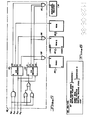
- FIG. 1 there is shown a block diagram of a data processing system in which the present invention can be employed.
- a microprocessor (up) 10 is operatively connected to a bus 20, having data and address lines.
- a memory 30 and a peripheral controller 40 are also operatively connected to the bus 20.
- a peripheral device 45 is operatively connected to the peripheral controller 40.
- the preferred embodiment of the present invention specifically shows a disk controller and a disk device for the peripheral controller 40 and the peripheral 45, respectively, it will be understood by those skilled in the art that the present invention is applicable to a wide variety of peripheral controllers and peripheral devices.
- the peripheral controller 40 includes a buffer (or peripheral register) 41 which temporarily stores data from the bus 20 or from the peripheral 45.
- the discussion hereinunder focuses on transfers between the peripheral controller 40 and the data processing system, i.e., the memory 30 and the microprocessor 10, to specifically cover the peripheral controller 40 - data processing system interface rather than the peripheral controller 40 - peripheral device 45 interface
- FIG. 2 there is shown a memory map of the preferred embodiment of the present invention.
- the memory 30 (also referred to herein as memory modules) of the data processing system of the preferred embodiment of the present invention is mapped to four 16K segments, the four segments forming a total memory space. Sixteen address lines A 15 - Ao where A 0 is the least significant bit, are utilized in bus 20.
- the upper 16K (locations C000 - FFFF hexadecimal, all memory locations given herein are in hexadecimal) is mapped to include a 4K ROM from locations F000 - FFFF, and 8K RAM from locations D000 to EFFF, and an I/O register at location C000.
- address bits A 15 and A 14 are both a logic one. This upper 16K of memory is also referred to herein as the first 16K of memory.
- the next, or second, 16K of the defined memory map from location 8000 to BFFF includes a 4K ROM image, an 8K RAM image, and an I/O register image which mirrors (or duplicates) the first 16K.
- a 15 is a logic one and A 14 is a logic zero.
- the third 16K of the defined memory map from locations 4000 to 7FFF also includes a 4K ROM image, an 8K RAM image and an I/O register image which mirrors the upper 16K.
- a 15 is a logic zero and A 14 is a logic one.
- the fourth (or lower) 16K of the defined memory map from locations 0000 to 3FFF is not utilized in the preferred embodiment of the present invention.
- the second 16K of memory is addressed when a data movement is to be performed from the peripheral register 41 to RAM memory, and the third 16K of memory is addressed when a data move operation is to be performed from memory to the peripheral register 41. This operation will be described in further detail hereinunder.
- the addresses 0000-FFFF are the memory space addresses within the total memory space.
- Memory 30 of the preferred embodiment of the present invention includes a 4K ROM memory module 30-3 having real addresses 000 - FFF, a first 4K RAM1 memory module 30-1 having real addresses 000 - FFF, and a second 4K RAM2 memory module 30-2 having real addresses 000 - FFF and further having pseudo addresses 1000 - 1FFF.
- Address lines 21, All - Ao of bus 20, are operatively connected to the corresponding 12 terminals of the ROM 30-3, RAM1 30-1 and RAM2 30-2. These 12 address lines which carry the corresponding address signals from microprocessor 10 are sufficient to address any location within a 4K space.
- a 15 , and A 14 are the upper bits utilized to address one of the 16K areas, and A 13 , A 12 are utilized to address the area within the selected 16K area.
- an enable signal is coupled from control logic 50.
- the control logic 50 generates the proper enable signal by decoding address information contained on address lines A 15 - A 12 , the control logic 50 to be described in detail hereinunder.
- An enable signal from control logic 50 is also coupled to an enable terminal, E, of peripheral register 41.
- Data lines 22 of bus 20 are connected to the corresponding data terminals, D, of the ROM and RAM memory modules and the data terminals of the peripheral register 41. It will be understood that if more than a single peripheral register 41 is utilized in the peripheral controller 40, address lines 21 can be coupled to corresponding address terminals of the peripheral registers (not shown) in order to address a single peripheral register.
- FIG. 4A and 4B which together make up Figure 4, there is shown a block diagram of a multiplexer, MUX, 51 which switches the control signals from the control logic 50 to the appropriate memory module 30 and/or peripheral register 41, thereby achieving the desired operation.
- the microprocessor read strobe signal is connected to input terminal A0, C0, Bl, A2, B2, and C3.
- Input terminal B0, Cl, C2, and B3 are tied to a logic zero which is effectively a disabling signal.
- the microprocessor write strobe signal is connected to input terminals Al and A3.
- the output of MUX 51, outputs 0 - 3 are connected to the RAM/ROM read strobe terminal of the memory modules 30, RAM write strobe terminal of RAM 30-1, 30-2, peripheral read strobe terminal, and peripheral write strobe terminal, respectively.
- Address signals A 15 and A 14 are utilized to select between input terminals A, B, and C, in accordance with the table of Figure 4B.
- the microprocessor 10 In a normal operation by the microprocessor 10 in which the microprocessor is accessing the memory modules 30 and/or the peripheral register 41, the microprocessor is addressing memory space in which A 15 and A 14 are a logic one. Hence, the A input terminals of MUX 51 are selected.
- the microprocessor read strobe signal is coupled to the RAM/ROM read strobe terminal and is also coupled to the peripheral read strobe terminal via output terminal 2.
- normal reads are made from the ROM 30-3, RAM 30-1, 30-2, or the peripheral register 41 by the microprocessor 10.
- the microprocessor 10 again addresses address space is which A 15 and A 14 are both a logic one and the write strobe signal is coupled to the RAM write strobe terminal or the peripheral write strobe terminal as a function of the particular address, thereby performing normal write operations to the RAM 30-1, 30-2 or the peripheral register 41.
- the microprocessor 10 also acts as a controller.
- the peripheral register 41 has data to be transferred, assuming a read operation of the peripheral device 45, the data ready signal is generated by the peripheral controller 40, thereby interrupting the microprocessor 10.
- the microprocessor 10 then causes the data stored in peripheral register 41 to be directly inputted into memory bypassing the operation of reading the data into an internal register of the microprocessor and then outputting the data into memory 30.
- the microprocessor performs a "dummy read" of the RAM address in which the data is to be stored.
- the address space addressed is the second 16K of the defined memory map in which A 15 and A 14 are a logic one and a logic zero, respectively. This causes the B input terminals of MUX51 to be selected.
- the "dummy read” from the microprocessor causes the read strobe signal to be coupled via input Bl to the RAM write strobe terminal.
- the microprocessor "dummy read” also causes the read strobe signal to be coupled via input B2 to the peripheral read strobe terminal, the peripheral write strobe being disabled by the logic zero input via input B3.
- the peripheral operation is a read, or output of the data, the data being placed on the data lines 22 and the RAM accepts the data that is present on the data lines 22 and is written into the RAM at the address specified on the address lines, the address being the address of the "dummy read” operation.
- data is transferred directly from the peripheral register 41 into the RAM and bypasses the transfer of the data into the microprocessor 10.
- RAM1 30-1 and RAM2 30-2 both have addresses corresponding to the address on the address line but only a single RAM, i.e., either RAMl or RAM2, is selected as a function of the enable signal.
- the generation of the proper enable signal to select the correct RAM, i.e., RAM1 or RAM2, will be discussed hereinunder.
- the microprocessor When a write operation from memory to the peripheral register 41 is to be performed, the microprocessor performs a "dummy read" operation of the address in memory to be read, and addresses the third 16K area in which A 15 is a logic zero and A 14 is a logic one, this area having been defined as the data move from memory to the peripheral, this having been described in conjunction with Figure 2 above. In this memory space input terminals C are selected.
- the microprocessor "dummy read” causes the microprocessor read strobe signal to be coupled to the RAM read terminal and also causes the microprocessor read strobe signal to be coupled to the peripheral write terminal.
- the data is placed on the data lines 22 from the RAM and the data present on the data lines 22 is written into the peripheral register 41.
- the enable signals coupled to the memory modules 30 cause data from a single RAM 30-1, 30-2, or ROM 30-3 to place data on the data lines 22.
- This operation again bypasses the microprocessor having to read the data into an internal register and then outputting the data to the peripheral controller 41.
- the logic zero connected to the input terminals assures the control signal is zero, disabling the particular function.
- the D input terminals of MUX51 are not utilized in the preferred embodiment of the present invention.
- enable logic 52 of the control logic 50 generates an enable signal for each of the memory modules 30-1, 30-2, 30-3, and for the peripheral register 41, the enable signal being coupled to the corresponding enable terminal, E, of each module.
- the first 16K address space is utilized and A 15 and A 14 are both a logic one, enabling a first (2:4) decoder 53.
- the decoder decodes the signals associated with address lines A 13 and A 12 . These two signals identify the particular module being addressed.
- the first decoder 53 decodes A 13 as a logic one and A 12 as a logic zero generating an enable signal which enables OR gate 56 thereby allowing accesses to RAM2 30-2.
- a second (2:4) decoder 54 is enabled which enables either RAMl 30-1 or RAM2 30-2 as a function of the address information signals on address lines A 13 and A 12 , the corresponding enable signal being coupled to the OR gate 57 for enabling the peripheral register 41 and the corresponding R AMI or RAM2.
- a read or write operation of the peripheral register 41 or the RAM 30-1, 30-2 is a function of the control signals from the multiplexer 51.
- FIG. 6 there is shown the operations performed by the interrupt routine of the microprocessor.
- the data ready signal is generated and is coupled to the interrupt terminal of the microprocessor 10.
- the microprocessor performs the operations of the interrupt routine of Figure 6. Namely, a first overhead operation is performed which requires saving the machine state and initializing a pointer which defines the memory location in which the data is to be stored. A "dummy read" is then performed to the location in which a data access is to be made, the location being defined in address bits A 13 - Ao . The address space addressed by bits A 13 - Ao is sufficient to address any location within the defined 16K.
- a 15 and A 14 are included in the address signals placed on the address lines 21 which define which operation is to be performed, the type of operation being equated to one of four 16K areas as defined by the memory map as discussed above.
- the second overhead operation is executed which essentially restores the pointer and restores the machine state.
- the interrupt routine is exited and the microprocessor continues to perform or execute its application program or task which was underway prior to the interrupt.
- a Motorola 68000 microprocessor is utilized, and the steps required to perform the various overhead operation are minimized. This reduces the amount of overhead, thereby reducing the amount of time within the interrupt routine.
Landscapes
- Engineering & Computer Science (AREA)
- Theoretical Computer Science (AREA)
- Physics & Mathematics (AREA)
- General Engineering & Computer Science (AREA)
- General Physics & Mathematics (AREA)
- Microcomputers (AREA)
- Bus Control (AREA)
- Combined Controls Of Internal Combustion Engines (AREA)
- Dram (AREA)
- Information Transfer Systems (AREA)
- Hardware Redundancy (AREA)
- Stabilization Of Oscillater, Synchronisation, Frequency Synthesizers (AREA)
Abstract
Description
- This invention relates to information movement within a data processing system generally between a memory unit of the data processing system and a peripheral, and more specifically, relates to a microprocessor based input/output (I/O) controller.
- Microprocessor based systems, especially those used as intelligent peripheral controllers, are often faced with a time critical data movement problem. In its simplest form, this problem is one of moving data from a buffer in a peripheral controller device (which appears to the microprocessor as a single location in a memory map) to an ordered array of sequential locations in memory (RAM).
- In present systems, the peripheral controller device is usually equipped with a control line to indicate that data in the buffer is ready to be moved. This control line is usually connected to an interrupt terminal of the microprocessor. Upon the occurrence of a data ready signal at the interrupt terminal, the microprocessor causes a plurality of operations to be performed. These operations include saving the state of the machine (i.e., the microprocessor). Data is moved from the buffer of the peripheral controller to an internal register of the microprocessor. Next, an index register is loaded with a previously saved pointer, and then the data is moved from the internal register to a location in RAM pointed to by the index register. The quantity in the index register is incremented and saved for the next data movement, and finally the machine is restored to the state existing before the interrupt occurred.
- If there is sufficient time to execute all of these steps before the peripheral controller device has a data over-run, this method of data movement is simple and works very well. But, as data transfer speeds increase, especially in high density floppy, winchester or communications applications, the microprocessor will run out of time to perform all of the above operations before the next piece or quantum (usually a byte or a word) of data is available.
- Hence, there is a need to provide an apparatus for performing the desired data movement at the high speed transfer rates required in the aforementioned applications.
- Therefore, it is the object of the present invention to provide an apparatus to perform a data move operation with significantly reduced steps thereby reducing the time required to perform the data move operation.
- It is a further object of the present invention to provide an apparatus to perform a high speed data move operation.
- These and other objects of the present invention are achieved by the invention as characterized in claim 1 and will become more apparent when taken in conjunction with the following description and attached drawings showing a preferred embodiment of the invention.
- According to the invention in a data processing system an apparatus is provided for controlling data movement between a peripheral and the data processing system. The apparatus comprises a memory for storing data, wherein the memory comprises a plurality of memory modules, each memory module having a plurality of addressable locations. Each memory module corresponds to an assigned area of a first memory map, the first memory map being duplicated into a plurality of mirrored memory maps. Each mirrored memory map corresponds to a predefined operation, and further a composite of the first memory map and the plurality of mirrored memory maps form a total memory space. Each memory location within the total memory space is defined by a unique memory space address. A processor performs a pseudo operation in response to a first control signal from the peripheral indicating data is available for being moved. A logic circuit operatively connected to the memory, the processor, and the peripheral, generates at least one control signal in response to the pseudo operation such that a predetermined data movement operation occurs.
-
- Figure 1 shows a block diagram of a data processing system in which the present invention can be employed;
- Figure 2 shows a defined memory map of the preferred embodiment of the present invention;
- Figure 3 shows a block diagram of physical memory of the preferred embodiment of the present invention;
- Figure 4, which is comprised of Figures 4A and 4B, shows input and output connections to a multiplexer for switching control signals thereby activating the appropriate circuitry to accomplish the desired operation;
- Figure 5 shows a logic block diagram of enable logic; and
- Figure 6 shows the steps in an interrupt routine performed by a microprocessor of the data processing system of the preferred embodiment of the present invention to initiate the data move operation.
- Referring to Figure 1, there is shown a block diagram of a data processing system in which the present invention can be employed. A microprocessor (up) 10 is operatively connected to a
bus 20, having data and address lines. A memory 30 and aperipheral controller 40 are also operatively connected to thebus 20. Aperipheral device 45 is operatively connected to theperipheral controller 40. Although, the preferred embodiment of the present invention specifically shows a disk controller and a disk device for theperipheral controller 40 and the peripheral 45, respectively, it will be understood by those skilled in the art that the present invention is applicable to a wide variety of peripheral controllers and peripheral devices. Theperipheral controller 40 includes a buffer (or peripheral register) 41 which temporarily stores data from thebus 20 or from the peripheral 45. The discussion hereinunder focuses on transfers between theperipheral controller 40 and the data processing system, i.e., the memory 30 and themicroprocessor 10, to specifically cover the peripheral controller 40 - data processing system interface rather than the peripheral controller 40 -peripheral device 45 interface - Referring to Figure 2, there is shown a memory map of the preferred embodiment of the present invention. The memory 30 (also referred to herein as memory modules) of the data processing system of the preferred embodiment of the present invention is mapped to four 16K segments, the four segments forming a total memory space. Sixteen address lines A15 - Ao where A0 is the least significant bit, are utilized in
bus 20. The upper 16K (locations C000 - FFFF hexadecimal, all memory locations given herein are in hexadecimal) is mapped to include a 4K ROM from locations F000 - FFFF, and 8K RAM from locations D000 to EFFF, and an I/O register at location C000. For this defined upper 16K of memory, address bits A15 and A14 are both a logic one. This upper 16K of memory is also referred to herein as the first 16K of memory. - The next, or second, 16K of the defined memory map from
location 8000 to BFFF includes a 4K ROM image, an 8K RAM image, and an I/O register image which mirrors (or duplicates) the first 16K. In the second 16K of defined memory, A15 is a logic one and A14 is a logic zero. The third 16K of the defined memory map fromlocations 4000 to 7FFF also includes a 4K ROM image, an 8K RAM image and an I/O register image which mirrors the upper 16K. In the third 16K of defined memory, A15 is a logic zero and A14 is a logic one. The fourth (or lower) 16K of the defined memory map fromlocations 0000 to 3FFF is not utilized in the preferred embodiment of the present invention. The second 16K of memory is addressed when a data movement is to be performed from theperipheral register 41 to RAM memory, and the third 16K of memory is addressed when a data move operation is to be performed from memory to theperipheral register 41. This operation will be described in further detail hereinunder. The addresses 0000-FFFF are the memory space addresses within the total memory space. - Referring to Figure 3, there is shown a block diagram of physical memory 30 of the preferred embodiment of the present invention. Memory 30 of the preferred embodiment of the present invention includes a 4K ROM memory module 30-3 having real addresses 000 - FFF, a first 4K RAM1 memory module 30-1 having real addresses 000 - FFF, and a second 4K RAM2 memory module 30-2 having real addresses 000 - FFF and further having pseudo addresses 1000 - 1FFF. Address lines 21, All - Ao of
bus 20, are operatively connected to the corresponding 12 terminals of the ROM 30-3, RAM1 30-1 and RAM2 30-2. These 12 address lines which carry the corresponding address signals frommicroprocessor 10 are sufficient to address any location within a 4K space. A15, and A14 are the upper bits utilized to address one of the 16K areas, and A13, A12 are utilized to address the area within the selected 16K area. In order to avoid memory accesses to a location within the multiple 4K areas, an enable signal is coupled fromcontrol logic 50. Thecontrol logic 50 generates the proper enable signal by decoding address information contained on address lines A15 - A12, thecontrol logic 50 to be described in detail hereinunder. An enable signal fromcontrol logic 50 is also coupled to an enable terminal, E, ofperipheral register 41.Data lines 22 ofbus 20 are connected to the corresponding data terminals, D, of the ROM and RAM memory modules and the data terminals of theperipheral register 41. It will be understood that if more than a singleperipheral register 41 is utilized in theperipheral controller 40, address lines 21 can be coupled to corresponding address terminals of the peripheral registers (not shown) in order to address a single peripheral register. - Referring to Figure 4A and 4B, which together make up Figure 4, there is shown a block diagram of a multiplexer, MUX, 51 which switches the control signals from the
control logic 50 to the appropriate memory module 30 and/orperipheral register 41, thereby achieving the desired operation. The microprocessor read strobe signal is connected to input terminal A0, C0, Bl, A2, B2, and C3. Input terminal B0, Cl, C2, and B3 are tied to a logic zero which is effectively a disabling signal. The microprocessor write strobe signal is connected to input terminals Al and A3. The output of MUX 51, outputs 0 - 3 are connected to the RAM/ROM read strobe terminal of the memory modules 30, RAM write strobe terminal of RAM 30-1, 30-2, peripheral read strobe terminal, and peripheral write strobe terminal, respectively. Address signals A15 and A14 are utilized to select between input terminals A, B, and C, in accordance with the table of Figure 4B. In a normal operation by themicroprocessor 10 in which the microprocessor is accessing the memory modules 30 and/or theperipheral register 41, the microprocessor is addressing memory space in which A15 and A14 are a logic one. Hence, the A input terminals of MUX 51 are selected. In this case the microprocessor read strobe signal is coupled to the RAM/ROM read strobe terminal and is also coupled to the peripheral read strobe terminal viaoutput terminal 2. Hence, normal reads are made from the ROM 30-3, RAM 30-1, 30-2, or theperipheral register 41 by themicroprocessor 10. When write operations are performed, themicroprocessor 10 again addresses address space is which A15 and A14 are both a logic one and the write strobe signal is coupled to the RAM write strobe terminal or the peripheral write strobe terminal as a function of the particular address, thereby performing normal write operations to the RAM 30-1, 30-2 or theperipheral register 41. - In an I/O operation, the
microprocessor 10 also acts as a controller. When theperipheral register 41 has data to be transferred, assuming a read operation of theperipheral device 45, the data ready signal is generated by theperipheral controller 40, thereby interrupting themicroprocessor 10. Themicroprocessor 10 then causes the data stored inperipheral register 41 to be directly inputted into memory bypassing the operation of reading the data into an internal register of the microprocessor and then outputting the data into memory 30. The microprocessor performs a "dummy read" of the RAM address in which the data is to be stored. The address space addressed is the second 16K of the defined memory map in which A15 and A14 are a logic one and a logic zero, respectively. This causes the B input terminals of MUX51 to be selected. The "dummy read" from the microprocessor causes the read strobe signal to be coupled via input Bl to the RAM write strobe terminal. The microprocessor "dummy read" also causes the read strobe signal to be coupled via input B2 to the peripheral read strobe terminal, the peripheral write strobe being disabled by the logic zero input via input B3. Hence, the peripheral operation is a read, or output of the data, the data being placed on the data lines 22 and the RAM accepts the data that is present on the data lines 22 and is written into the RAM at the address specified on the address lines, the address being the address of the "dummy read" operation. Hence, data is transferred directly from theperipheral register 41 into the RAM and bypasses the transfer of the data into themicroprocessor 10. RAM1 30-1 and RAM2 30-2 both have addresses corresponding to the address on the address line but only a single RAM, i.e., either RAMl or RAM2, is selected as a function of the enable signal. The generation of the proper enable signal to select the correct RAM, i.e., RAM1 or RAM2, will be discussed hereinunder. When a write operation from memory to theperipheral register 41 is to be performed, the microprocessor performs a "dummy read" operation of the address in memory to be read, and addresses the third 16K area in which A15 is a logic zero and A14 is a logic one, this area having been defined as the data move from memory to the peripheral, this having been described in conjunction with Figure 2 above. In this memory space input terminals C are selected. In this case the microprocessor "dummy read" causes the microprocessor read strobe signal to be coupled to the RAM read terminal and also causes the microprocessor read strobe signal to be coupled to the peripheral write terminal. Hence, the data is placed on the data lines 22 from the RAM and the data present on the data lines 22 is written into theperipheral register 41. Again, the enable signals coupled to the memory modules 30 cause data from a single RAM 30-1, 30-2, or ROM 30-3 to place data on the data lines 22. This operation again bypasses the microprocessor having to read the data into an internal register and then outputting the data to theperipheral controller 41. The logic zero connected to the input terminals assures the control signal is zero, disabling the particular function. The D input terminals of MUX51 are not utilized in the preferred embodiment of the present invention. - Referring to Figure 5, there is shown a block diagram of enable logic 52 of the
control logic 50. The enable logic 52 generates an enable signal for each of the memory modules 30-1, 30-2, 30-3, and for theperipheral register 41, the enable signal being coupled to the corresponding enable terminal, E, of each module. When themicroprocessor 10 is accessing the memory modules 30 or theperipheral register 41, the first 16K address space is utilized and A15 and A14 are both a logic one, enabling a first (2:4)decoder 53. The decoder decodes the signals associated with address lines A13 and A12. These two signals identify the particular module being addressed. Hence when A13 is a logic zero and A12 is a logic zero, theperipheral register 41 is being addressed by the microprocessor, and the enable signal is coupled to theperipheral register 41 via anOR gate 57. When A13 and A12 are both a logic one, the ROM module 30-3 is being addressed and the enable signal is directly coupled to the ROM. When the RAM is being addressed by themicroprocessor 10, for address locations between D000 and DFFF, A13 is a logic zero and A12 is a logic one, thereby generating an enable signal which enables ORgate 55 allowing accesses to RAM1 30-1. Similarly, when the microprocessor is addressing memory locations E000 through EFFF of RAM thefirst decoder 53 decodes A13 as a logic one and A12 as a logic zero generating an enable signal which enables OR gate 56 thereby allowing accesses to RAM2 30-2. In the movement of data between theperipheral register 41 and the RAMS 30-1, 30-2, a second (2:4)decoder 54 is enabled which enables either RAMl 30-1 or RAM2 30-2 as a function of the address information signals on address lines A13 and A12, the corresponding enable signal being coupled to theOR gate 57 for enabling theperipheral register 41 and the corresponding RAMI or RAM2. A read or write operation of theperipheral register 41 or the RAM 30-1, 30-2 is a function of the control signals from the multiplexer 51. - Referring to Figure 6, there is shown the operations performed by the interrupt routine of the microprocessor. As discussed before, when the
peripheral register 41 is full and contains data ready to be transferred, the data ready signal is generated and is coupled to the interrupt terminal of themicroprocessor 10. The microprocessor performs the operations of the interrupt routine of Figure 6. Namely, a first overhead operation is performed which requires saving the machine state and initializing a pointer which defines the memory location in which the data is to be stored. A "dummy read" is then performed to the location in which a data access is to be made, the location being defined in address bits A13 - Ao. The address space addressed by bits A13 - Ao is sufficient to address any location within the defined 16K. A15 and A14 are included in the address signals placed on the address lines 21 which define which operation is to be performed, the type of operation being equated to one of four 16K areas as defined by the memory map as discussed above. Once the "dummy read" operation is performed, the second overhead operation is executed which essentially restores the pointer and restores the machine state. Then the interrupt routine is exited and the microprocessor continues to perform or execute its application program or task which was underway prior to the interrupt. In the preferred embodiment of the present invention, a Motorola 68000 microprocessor is utilized, and the steps required to perform the various overhead operation are minimized. This reduces the amount of overhead, thereby reducing the amount of time within the interrupt routine. This reduction in overhead allows the microprocessor to perform its task and also act as a direct memory access controller and not encounter an over-run condition. (An over-run condition occurs when the next piece or quantum of data is available in theperipheral register 41 before the microprocessor has had a chance to move the previous piece of data.) It will be understood by those skilled in the art that outputting data from memory 30 to the peripheral register 41 a similar operation is performed. Namely, a data request signal from the peripheral register is coupled to themicroprocessor 10 which results in an interrupt to themicroprocessor 10. A "dummy read" in the interrupt routine is then performed from the third 16K memory space in which A15 is a logic zero and A14 is a logic one.
Claims (3)
Applications Claiming Priority (2)
| Application Number | Priority Date | Filing Date | Title |
|---|---|---|---|
| US06/750,797 US4764896A (en) | 1985-07-01 | 1985-07-01 | Microprocessor assisted memory to memory move apparatus |
| US750797 | 1985-07-01 |
Publications (3)
| Publication Number | Publication Date |
|---|---|
| EP0212152A2 true EP0212152A2 (en) | 1987-03-04 |
| EP0212152A3 EP0212152A3 (en) | 1988-08-24 |
| EP0212152B1 EP0212152B1 (en) | 1993-05-19 |
Family
ID=25019201
Family Applications (1)
| Application Number | Title | Priority Date | Filing Date |
|---|---|---|---|
| EP86108812A Expired - Lifetime EP0212152B1 (en) | 1985-07-01 | 1986-06-28 | Microprocessor assisted memory to memory move apparatus |
Country Status (8)
| Country | Link |
|---|---|
| US (1) | US4764896A (en) |
| EP (1) | EP0212152B1 (en) |
| JP (1) | JPS629456A (en) |
| AU (1) | AU591126B2 (en) |
| CA (1) | CA1261071A (en) |
| DE (1) | DE3688446T2 (en) |
| NO (1) | NO176294C (en) |
| ZA (1) | ZA863644B (en) |
Cited By (3)
| Publication number | Priority date | Publication date | Assignee | Title |
|---|---|---|---|---|
| EP0426156A2 (en) * | 1989-11-03 | 1991-05-08 | Compaq Computer Corporation | Floppy disk controller with DMA verify operations |
| EP0501621A2 (en) * | 1991-02-26 | 1992-09-02 | Hewlett-Packard Company | Address prediction and verification for burst cycle data reads |
| EP0715252A1 (en) * | 1994-11-14 | 1996-06-05 | Nec Corporation | A bit field peripheral |
Families Citing this family (10)
| Publication number | Priority date | Publication date | Assignee | Title |
|---|---|---|---|---|
| JPS638491Y2 (en) * | 1980-10-08 | 1988-03-14 | ||
| US4987530A (en) * | 1985-11-15 | 1991-01-22 | Data General Corp. | Input/output controller for a data processing system |
| JPS63255759A (en) * | 1987-04-14 | 1988-10-24 | Mitsubishi Electric Corp | Control system |
| JPS63255760A (en) * | 1987-04-14 | 1988-10-24 | Mitsubishi Electric Corp | Control system |
| CA2099838C (en) * | 1993-07-05 | 2000-01-18 | Philip Ching | Method of extracting data words from a binary serial bit stream |
| US5664152A (en) * | 1995-06-06 | 1997-09-02 | Hewlett-Packard Company | Multiple segmenting of main memory to streamline data paths in a computing system |
| US5724502A (en) * | 1995-08-07 | 1998-03-03 | International Business Machines Corporation | Test mode matrix circuit for an embedded microprocessor core |
| DE19946716A1 (en) * | 1999-09-29 | 2001-04-12 | Infineon Technologies Ag | Process for operating a processor bus |
| US7132963B2 (en) * | 2004-09-13 | 2006-11-07 | Ati Technologies Inc. | Methods and apparatus for processing variable length coded data |
| US9009114B1 (en) * | 2005-10-31 | 2015-04-14 | Symantec Operating Corporation | Version mapped incremental backups |
Citations (3)
| Publication number | Priority date | Publication date | Assignee | Title |
|---|---|---|---|---|
| EP0026648A2 (en) * | 1979-09-26 | 1981-04-08 | Sperry Corporation | Digital data transfer apparatus |
| JPS5972532A (en) * | 1982-10-20 | 1984-04-24 | Hitachi Ltd | Data transfer control method |
| EP0117836A2 (en) * | 1983-03-01 | 1984-09-05 | STMicroelectronics, Inc. | Address-controlled automatic bus arbitration and address modification |
Family Cites Families (8)
| Publication number | Priority date | Publication date | Assignee | Title |
|---|---|---|---|---|
| US4316244A (en) * | 1978-11-08 | 1982-02-16 | Data General Corporation | Memory apparatus for digital computer system |
| US4371932A (en) * | 1979-07-30 | 1983-02-01 | International Business Machines Corp. | I/O Controller for transferring data between a host processor and multiple I/O units |
| JPS56116138A (en) * | 1980-02-15 | 1981-09-11 | Omron Tateisi Electronics Co | Input and output controller |
| US4476522A (en) * | 1981-03-09 | 1984-10-09 | International Business Machines Corporation | Programmable peripheral processing controller with mode-selectable address register sequencing |
| US4454575A (en) * | 1980-12-29 | 1984-06-12 | International Business Machines Corporation | Shared memory system with access by specialized peripherals managed by controller initialized by supervisory CPU |
| US4450521A (en) * | 1981-04-13 | 1984-05-22 | Texas Instruments Incorporated | Digital processor or microcomputer using peripheral control circuitry to provide multiple memory configurations and offset addressing capability |
| US4535404A (en) * | 1982-04-29 | 1985-08-13 | Honeywell Information Systems Inc. | Method and apparatus for addressing a peripheral interface by mapping into memory address space |
| US4620279A (en) * | 1983-07-29 | 1986-10-28 | Standard Oil Company, Now Amoco Corporation | Data transfer system |
-
1985
- 1985-07-01 US US06/750,797 patent/US4764896A/en not_active Expired - Fee Related
-
1986
- 1986-04-28 NO NO861662A patent/NO176294C/en unknown
- 1986-05-14 CA CA000509177A patent/CA1261071A/en not_active Expired
- 1986-05-16 ZA ZA863644A patent/ZA863644B/en unknown
- 1986-05-19 AU AU57552/86A patent/AU591126B2/en not_active Ceased
- 1986-06-28 DE DE86108812T patent/DE3688446T2/en not_active Expired - Fee Related
- 1986-06-28 EP EP86108812A patent/EP0212152B1/en not_active Expired - Lifetime
- 1986-07-01 JP JP61154962A patent/JPS629456A/en active Pending
Patent Citations (3)
| Publication number | Priority date | Publication date | Assignee | Title |
|---|---|---|---|---|
| EP0026648A2 (en) * | 1979-09-26 | 1981-04-08 | Sperry Corporation | Digital data transfer apparatus |
| JPS5972532A (en) * | 1982-10-20 | 1984-04-24 | Hitachi Ltd | Data transfer control method |
| EP0117836A2 (en) * | 1983-03-01 | 1984-09-05 | STMicroelectronics, Inc. | Address-controlled automatic bus arbitration and address modification |
Non-Patent Citations (1)
| Title |
|---|
| PATENT ABSTRACTS OF JAPAN, vol. 8, no. 179 (P-295)[1616], 17th August 1984; & JP-A-59 072 532 (HITACHI SEISAKUSHO K.K.) 24-04-84 * |
Cited By (6)
| Publication number | Priority date | Publication date | Assignee | Title |
|---|---|---|---|---|
| EP0426156A2 (en) * | 1989-11-03 | 1991-05-08 | Compaq Computer Corporation | Floppy disk controller with DMA verify operations |
| EP0426156A3 (en) * | 1989-11-03 | 1995-03-15 | Compaq Computer Corp | Floppy disk controller with dma verify operations |
| US5442753A (en) * | 1989-11-03 | 1995-08-15 | Compaq Computer Corp. | Circuitry for providing replica data transfer signal during DMA verify operations |
| EP0501621A2 (en) * | 1991-02-26 | 1992-09-02 | Hewlett-Packard Company | Address prediction and verification for burst cycle data reads |
| EP0501621A3 (en) * | 1991-02-26 | 1994-07-06 | Hewlett Packard Co | Address prediction and verification for burst cycle data reads |
| EP0715252A1 (en) * | 1994-11-14 | 1996-06-05 | Nec Corporation | A bit field peripheral |
Also Published As
| Publication number | Publication date |
|---|---|
| DE3688446T2 (en) | 1994-01-05 |
| US4764896A (en) | 1988-08-16 |
| JPS629456A (en) | 1987-01-17 |
| NO176294C (en) | 1995-03-08 |
| CA1261071A (en) | 1989-09-26 |
| EP0212152A3 (en) | 1988-08-24 |
| EP0212152B1 (en) | 1993-05-19 |
| NO861662L (en) | 1987-01-02 |
| DE3688446D1 (en) | 1993-06-24 |
| ZA863644B (en) | 1986-12-30 |
| AU5755286A (en) | 1987-01-08 |
| NO176294B (en) | 1994-11-28 |
| AU591126B2 (en) | 1989-11-30 |
Similar Documents
| Publication | Publication Date | Title |
|---|---|---|
| US4550368A (en) | High-speed memory and memory management system | |
| US4173783A (en) | Method of accessing paged memory by an input-output unit | |
| EP0979456B1 (en) | Memory access protection | |
| US4539637A (en) | Method and apparatus for handling interprocessor calls in a multiprocessor system | |
| US4386402A (en) | Computer with dual vat buffers for accessing a common memory shared by a cache and a processor interrupt stack | |
| US4382278A (en) | Hierarchial memory system with microcommand memory and pointer register mapping virtual CPU registers in workspace cache #4 and main memory cache | |
| JPS6259822B2 (en) | ||
| US4764896A (en) | Microprocessor assisted memory to memory move apparatus | |
| US5388230A (en) | Parallel processor having multi-processing units either connected or bypassed in either series or parallel by the use of bus switching | |
| US5146572A (en) | Multiple data format interface | |
| US4346441A (en) | Random access memory system for extending the memory addressing capacity of a CPU | |
| US4314332A (en) | Memory control system | |
| US5444852A (en) | I/O device interface having buffer mapped in processor memory addressing space and control registers mapped in processor I/O addressing space | |
| US5703810A (en) | DRAM for texture mapping | |
| EP0081358B1 (en) | Data processing system providing improved data transfer between modules | |
| US4814977A (en) | Apparatus and method for direct memory to peripheral and peripheral to memory data transfers | |
| EP0207472A2 (en) | Microprocessor assisted data block transfer apparatus | |
| KR900009212Y1 (en) | Address control apparatus | |
| JP2699482B2 (en) | Data transfer control device | |
| SU1541623A1 (en) | Device for interfacing computer with peripheral device | |
| JPH05108477A (en) | Memory access system | |
| EP0264740A2 (en) | Time partitioned bus arrangement | |
| JPH01219930A (en) | Interrupt control circuit device for indirect address system | |
| JPH0492935A (en) | Information processor | |
| JPS5819965A (en) | Recording device |
Legal Events
| Date | Code | Title | Description |
|---|---|---|---|
| PUAI | Public reference made under article 153(3) epc to a published international application that has entered the european phase |
Free format text: ORIGINAL CODE: 0009012 |
|
| AK | Designated contracting states |
Kind code of ref document: A2 Designated state(s): BE DE FR GB NL |
|
| PUAL | Search report despatched |
Free format text: ORIGINAL CODE: 0009013 |
|
| AK | Designated contracting states |
Kind code of ref document: A3 Designated state(s): BE DE FR GB NL |
|
| 17P | Request for examination filed |
Effective date: 19890127 |
|
| 17Q | First examination report despatched |
Effective date: 19890905 |
|
| GRAA | (expected) grant |
Free format text: ORIGINAL CODE: 0009210 |
|
| AK | Designated contracting states |
Kind code of ref document: B1 Designated state(s): BE DE FR GB NL |
|
| PGFP | Annual fee paid to national office [announced via postgrant information from national office to epo] |
Ref country code: FR Payment date: 19930616 Year of fee payment: 8 |
|
| REF | Corresponds to: |
Ref document number: 3688446 Country of ref document: DE Date of ref document: 19930624 |
|
| ET | Fr: translation filed | ||
| PGFP | Annual fee paid to national office [announced via postgrant information from national office to epo] |
Ref country code: DE Payment date: 19940319 Year of fee payment: 9 |
|
| PLBE | No opposition filed within time limit |
Free format text: ORIGINAL CODE: 0009261 |
|
| STAA | Information on the status of an ep patent application or granted ep patent |
Free format text: STATUS: NO OPPOSITION FILED WITHIN TIME LIMIT |
|
| PGFP | Annual fee paid to national office [announced via postgrant information from national office to epo] |
Ref country code: GB Payment date: 19940328 Year of fee payment: 9 |
|
| 26N | No opposition filed | ||
| PGFP | Annual fee paid to national office [announced via postgrant information from national office to epo] |
Ref country code: BE Payment date: 19940519 Year of fee payment: 9 |
|
| PGFP | Annual fee paid to national office [announced via postgrant information from national office to epo] |
Ref country code: NL Payment date: 19940630 Year of fee payment: 9 |
|
| PG25 | Lapsed in a contracting state [announced via postgrant information from national office to epo] |
Ref country code: FR Effective date: 19950228 |
|
| REG | Reference to a national code |
Ref country code: FR Ref legal event code: ST |
|
| PG25 | Lapsed in a contracting state [announced via postgrant information from national office to epo] |
Ref country code: GB Effective date: 19950628 |
|
| PG25 | Lapsed in a contracting state [announced via postgrant information from national office to epo] |
Ref country code: BE Effective date: 19950630 |
|
| BERE | Be: lapsed |
Owner name: HONEYWELL INC. Effective date: 19950630 |
|
| PG25 | Lapsed in a contracting state [announced via postgrant information from national office to epo] |
Ref country code: NL Effective date: 19960101 |
|
| GBPC | Gb: european patent ceased through non-payment of renewal fee |
Effective date: 19950628 |
|
| NLV4 | Nl: lapsed or anulled due to non-payment of the annual fee |
Effective date: 19960101 |
|
| PG25 | Lapsed in a contracting state [announced via postgrant information from national office to epo] |
Ref country code: DE Effective date: 19960301 |
|
| APAH | Appeal reference modified |
Free format text: ORIGINAL CODE: EPIDOSCREFNO |