EP0026648A2 - Digital data transfer apparatus - Google Patents
Digital data transfer apparatus Download PDFInfo
- Publication number
- EP0026648A2 EP0026648A2 EP80303386A EP80303386A EP0026648A2 EP 0026648 A2 EP0026648 A2 EP 0026648A2 EP 80303386 A EP80303386 A EP 80303386A EP 80303386 A EP80303386 A EP 80303386A EP 0026648 A2 EP0026648 A2 EP 0026648A2
- Authority
- EP
- European Patent Office
- Prior art keywords
- data
- microprocessor
- computer
- transfer
- computing device
- Prior art date
- Legal status (The legal status is an assumption and is not a legal conclusion. Google has not performed a legal analysis and makes no representation as to the accuracy of the status listed.)
- Granted
Links
- 230000015654 memory Effects 0.000 claims abstract description 49
- 230000004044 response Effects 0.000 claims abstract description 5
- 238000013500 data storage Methods 0.000 claims 2
- 238000010586 diagram Methods 0.000 description 8
- 230000000694 effects Effects 0.000 description 6
- 101150066014 PUP1 gene Proteins 0.000 description 3
- 238000013507 mapping Methods 0.000 description 3
- 101150001846 PUP2 gene Proteins 0.000 description 1
- 230000002457 bidirectional effect Effects 0.000 description 1
- 230000006870 function Effects 0.000 description 1
- 238000012856 packing Methods 0.000 description 1
Images

Classifications
-
- G—PHYSICS
- G06—COMPUTING; CALCULATING OR COUNTING
- G06F—ELECTRIC DIGITAL DATA PROCESSING
- G06F15/00—Digital computers in general; Data processing equipment in general
- G06F15/16—Combinations of two or more digital computers each having at least an arithmetic unit, a program unit and a register, e.g. for a simultaneous processing of several programs
- G06F15/163—Interprocessor communication
- G06F15/167—Interprocessor communication using a common memory, e.g. mailbox
Definitions
- This invention relates to digital data transfer apparatus and may in particular be used to transfer data between two computing devices such as a computer and a microprocessor.
- the present invention provides an interface which utilizes internal instructions of the first computing device, such as a "block move” instruction for re-locating data within its local memory, to effect an external data transfer from its memory to that of the second computing device. Similarly, internal instructions are used for the transfer in the reverse direction.
- the hardware required for the digital transfer apparatus of the present invention is comparatively simple and comprises mainly appropriate registers for storing data or addresses, i.e. it uses well known components which are readily available.
- a map key register may be included in the interface to map data signals provided by the first computing device into addresses of the second computing device and thereby extend the available memory space.
- the transfer apparatus permits, e.g., the transfer of data in a direct memory access mode from the memory of a microprocessor to the memory of a minicomputer, and vice versa.
- a microprocessor 9 is provided with a control bus 10, an address bus 11 and a data bus 12.
- the bus 10 is a 14-bit control bus
- the bus 11 is a 16-bit address bus
- the bus 12 is an 8-bit bidirectional data bus.
- the busses are assumed to be associated with a Z80 microprocessor, although other microprocessors may be used instead.
- the minicomputer 16 is assumed to be of the Sperry Univac V70 series. Again, the invention may be used with other minicomputers.
- the minicomputer 16 is connected to the upper and lower byte tri-state busses 13 and 14, respectively, and to the address, data and control bus 15.
- the upper and lower byte busses 13 and 14 are provided since the microprocessor 9 produces an 8-bit data word and the computer 16 operates upon a 16-bit data word, with two bytes of data being required from the microprocessor 9 to form an appropriate data word for the computer 16.
- the computer 16 is connected to the bus 15 by a suitable connecting link 17 such as drivers or the like.
- a suitable connecting link 17 such as drivers or the like.
- the busses 13 and 14 are connected to the bus 15 by respective driver networks 19 and 18.
- Upper and lower byte data registers 20 and 21 are connected to receive 8-bit data words from the data bus 12 and to supply these 8-bit data words as the upper and lower bytes to the busses 13 and 14, respectively. Appropriate control signals are applied by control logic 30 (CTL) which is controlled by control bus 10.
- CTL control logic 30
- Upper and lower byte address registers 23 and 24 are also connected to receive input address signals from the bus 11 and to supply the output address signals to the busses 13 and 14, respectively.
- a map key register 22 is connected to receive mapping information from the data bus 12 and to supply same to the control bus 15 in order to control the mapping of the memory in computer 16.
- a suitable register 25 e.g., a FIFO memory
- the appropriate data bits are stored by the microprocessor 9 via data bus 12 in the upper and lower byte data registers 20 and 21. Subsequently, appropriate upper and lower byte address bits are supplied to the registers 23 and 24 by the microprocessor 9 via the bus 11. Also, the map key register 22 is set to the appropriate memory page by the microprocessor 9 along bus 12.
- a "block move" instruction is executed by the microprocessor 9, the information is externally transferred as described hereinafter. To the microprocessor 9, the operation is equivalent to relocating data from one portion of the microprocessor memory to another portion thereof. However, the data is actually redirected from the microprocessor memory and transferred in a direct memory access operation to the memory of the computer 16.
- data can be transferred directly from computer 16 to the microprocessor via register 25. That is, the 16-bit word is applied to register 25 by bus 15. The information is then supplied to bus 12 as two 8-bit bytes and stored in the memory of the microprocessor.
- FIG. 2 shows a more detailed diagram of the circuitry of the instant invention.
- the upper and lower byte data registers 20 and 21 are connected to the data bus 12.
- the inputs of the map key register 22 are also connected to the same data bus 12.
- the address bus 11 is connected to the inputs of the upper and lower byte address registers 23 and 24, respectively.
- the output terminals of the lower byte data register 21 and the lower byte address register 24 are connected together and to the bus 14.
- the output terminals of the upper byte data register 20 and the upper byte address register 23 are connected together and to the bus 13.
- the output terminals which form the busses 13, 14 and 15 are connected by appropriate driver networks 18 and 19 to the minicomputer bus 15, which is itself connected to the minicomputer 16 via the driver network 17.
- the data bits DO through D7 are applied to both the upper and lower byte data registers 20 and 21, respectively, via data bus 12.
- the bits DO through D7 are selected by the respective registers 20 and 21 at consecutive time periods as controlled by the signals supplied to the clock (CK) terminals of the respective registers.
- bits DO through D7 are first entered into the lower byte data register 21 in which the bits are latched and stored.
- the next 8-bit byte is applied as data bit DO-D7 to the upper byte data register 20 in which that information is then latched and stored.
- the output bits COBOO through COB07 are supplied from the lower byte register 21 to the bus 14 and then to the driver circuit 18.
- Output bits COB08 through COB15 are supplied from the upper byte register 20 via the bus 13 to the driver circuit 19. These signals are then supplied from the driver circuits 18 and 19 to the bus 15 ( Figure 1) where the bits are assembled into a 16-bit format and supplied to the computer 16.
- the data bits DO through D7 are supplied to the map key register 22 and, thence through the bus 15 to the minicomputer 16 as noted above.
- the map key register 22 permits appropriate mapping arrangements so that a greater memory capacity can be utilized in the system.
- the upper and lower byte address.registers 23 and 24 are connected to the address bus 11 to receive the address signals.
- the signals A09 through A15 are supplied to the upper byte address register 23 while the signals A01 through A08 are supplied to the lower byte address register 24.
- the output terminals of the registers 23 and 24 are connected to the driver registers 19 and 18 via the busses 13 and 14, respectively.
- DRY circuitry In order to assure proper control, the data-ready (DRY) status is controlled by DRY circuitry (not shown) which in turn generates the trap data input signal (TPDI) which is supplied to enable terminals (OE) of registers 20 and 21. Only during the DRY cycle can data be transferred from the registers 20 and 21 to the respective data busses 13 and 14.
- the FRY condition Conversely, only during the function-ready (FRY) condition are the address registers 23 and 24 and the map register 22 enabled.
- the FRY condition in turn, generates the trap address enable signal (TPADE) which is then supplied to the enable terminals ( ⁇ E) of registers 22, 23 and 24, enabling these registers to place the appropriate data onto the busses 13 and 14, respectively.
- TPADE trap address enable signal
- the FRY and DRY control circuits produce enabling signals at different times so that the data or address registers are enabled at different times.
- a load control circuit To control the clocking, and, thus, the loading of the data registers, a load control circuit is provided.
- This circuit includes a flip-flop 37, and inverting AND gates 35 and 36.
- the clear (CLR) terminal of flip-flop 37 is connected to receive the pull-up input signal PUP1.
- the initialization signal (INIT) is supplied to the pre-set (PRE) input terminal of flip-flop 37. With the application of this signal, flip-flop 37 is pre-set to the condition wherein the Q output terminal produces a high level signal and the Q terminal produces a low level signal.
- These signals are applied to one input terminal of each of the inverting NAND gates 35 and 36.
- the other input terminals of gates 35 and 36 are connected to receive the load controller output buffer control signal (LDCC ⁇ B).
- the address bus, registers 23 and 24, are similarly activated by the application of the C ⁇ ABST signal which is produced by an inverting NOR gate 41.
- One input terminal of the gate 41 is connected to the output terminal of an inverting AND gate 38 which receives the trap transfer (TPXFR) signal from the microprocessor 9 to indicate a DMA data transfer, and also the output signal from gate 35.
- the trap transfer signal is used only when DMA data are to be transferred.
- the gate 38 In the absence of the TPXFR signal, the gate 38 does not produce an output signal for causing DMA operation and, therefore, no DMA address is entered into the address registers 23 and 24.
- the gate 41 receives an output signal from inverting AND gate 39 which receives the pre-fetch input signal (PFFC) as well as the Q signal from a flip-flop 40 receives the PUP2 signal at its clear (CLR) input terminal.
- the C input terminal of the flip-flop 40 receives the TPXFR signal, while the D terminal receives the read/write command (CWR) signal which, during the initial DMA start-up cycle, activates the gate 39.
- the pre-set terminal (PRE) of flip-flop 40 is connected to the output terminal of gate 39 and the second input terminal gate 41. This has the effect of de-activating the latch flip-flop 40 after the first DMA cycle.
- the gate 39 With the application of the TPXFR signal, the status of the gate 38 and the ⁇ output of the flip-flop 40 are controlled. In addition, the signal level at one input terminal of the gate 41 is established via the gate 38. With the operation- of the flip-flop 40, the status of the gate 39 is also controlled. With the application of the pre-fetch signal (PFFC), the gate 39 provides signals to the flip-flop 40 and the gate 41 which control the output signal which is produced by the gate 41 and supplied to the registers 23 and 24 to establish the clocking operation relative thereto.
- PFFC pre-fetch signal
- Figure 3 shows a detailed circuit diagram for the computer-oriented circuitry.
- Figure 3 shows the trap logic as well as the execute command and data output decode interfacing circuitry.
- an inverting NOR gate 50 receives the TPDAE and the trap transfer (TPXFR) signals at its input terminals. These signals are supplied by the microprocessor and the computer control circuitry.
- the gate 50 supplies a reset trap request output signal (RTRQ) to the pre-set terminal of a flip-flop 51.
- RTRQ reset trap request output signal
- the CLR terminal of the flip-flop 51 receives the PUP1 signal referred to above.
- the D input terminal of flip-flop 51 is grounded, and the C input terminal receives the C ⁇ ABST signal from the gate 41 of Figure 2.
- the Q output terminal of flip-flop 51 is left unconnected, while the Q output terminal is connected to supply the trap request TPRQ signal to one input terminal of the trap logic circuit 52 which, together with the signal CWR, selects whether information is to be transferred to or from computer 16 by means of the trap-in (TPIX) and the trap-out (TPOX) signals respectively.
- the trap logic circuit 52 is connected to receive the interrupt clock IUCX signal, in addition the command read/write signal (CWR), from a computer receiver interface circuitry (not shown).
- the IUCX signal is used to synchronize the data transfer with the bus 15.
- trap logic circuit 52 produces the signal TPIX, which is supplied to the computer 16 when information data are to be transferred from the microprocessor 9 to the computer, and the output signal TPOX, which is supplied to the computer 16 when data are to be transferred from the computer memory to the microprocessor.
- FIG. 4 shows a detailed circuit diagram of the microprocessor bus control PROM 64 and the address decode logic used therewith.
- control logic circuit 62 receives control signals from the microprocessor I/O (input/output) port.
- the control logic circuit 62 supplies the data output signal (G ⁇ D) to the J terminal of flip-flop 63, and the block move control enable signal (BMCE) to the clock or toggle input terminal C of the flip-flop 63.
- the pre-set terminal receives the PUP1 signal while the clear (CLR) terminal receives the master reset signal (MRST).
- the Q output terminal of the flip-flop 63 is returned to the K input terminal thereof and, also, the terminal A4 of the bus control PROM 64.
- the A3 terminal of the PROM 64 receives the CWR signal while the A0 and A2 terminals receive the read (RD) and M1 signals, respectively.
- the write (WR) signal is supplied to terminal Al of PROM 64.
- the output terminals of the PROM 64 are connected to produce, on terminals QO through Q3, the signals LDC ⁇ B, F ⁇ RM, PFFC and PMRQ respectively.
- the PFFC signal is the pre-fetch signal referred to above in connection with Figure 2.
- the LDC ⁇ B signal is supplied to the gates 35, 36 and 37 of Figure 2.
- the FORM signal is supplied to the computer output buffer interface circuitry and controls operation of register 25 for transferring data and function signals from the computer 16 to the microprocessor 9.
- the PMRQ signal is supplied to an input terminal of the microprocessor memory 65.
- the PMRQ signal selectively enables or disables microprocessor memory 65 such that data is not returned to the local memory during a DMA transfer, or vice versa. That is, if the local memory is not disabled, the circuit acts as a "block-move" circuit and a block of data is relocated within the local memory. In this event, data is not transferred to the computer 16.
- operation of PROM 64 selectively causes the microprocessor to interface directly with the memory in the computer because the FORM signal enables appropriate tri-state drivers associated with the register 25.
- Table I below illustrates the basic operation of the bus control PROM 64.
- the PROM 64 receives five inputs and, thus, must operate on 32 possible combinations of signals. These combinations are numbered 0 (00000) to 31 (11111). These input signal combinations represent addresses for the PROM.
- the output signals represent the contents of the respective addresses which are listed. These output signals control the operation of the interfacing circuit. For example, the combination number 17 has the address 10001 and the output 1100. This combination indicates that input signals BMMC and RD are binary ones and the other input signals are binary zeroes.
- the output signals PMRQ and PFFC are binary ones and the other output signals are binary zeroes.
- FORM signal
- the microprocessor operation has not been particularly affected by the DMA operation. Data has been transferred directly from the computer memory to the microprocessor destination memory without requiring specifically dedicated microprocessor control signals.
- the microprocessor 9 performs a fetch cycle from its local memory, while the bus control PROM 65 enables .the register 25, disables the local memory and places instead the data from register 25 onto bus 12 for the microprocessor to pick up.
- the next DMA word is fetched from the memory of minicomputer 16.
- the microprocessor writes the data into the local memory to receive the data. It must be emphasised that the microprocessor only "knows" of and operates in its own memory space and its own domain. At no time does the microprocessor "realise" that a DMA operation is being performed between two separate systems. In this manner, software programs and hardware circuits can be designed in a simpler fashion. The same is true for the minicomputer.
- the microprocessor supplies the signal 00001 (combination 2) to the PROM 64 thereby indicating that a read (RD) operation is to occur.
- the gate 41 produces the C ⁇ ABST signal which sets the flip-flop 51 to produce the TP ⁇ X signal, and so cause the computer 16 to output data.
- computer 16 has made the microprocessor 9 read an address which is coincident with the first DMA address in the minicomputer memory.
- the address and the corresponding contents are applied to the busses 15 and 12, respectively.
- the C ⁇ ABST signal has, however, enabled the address registers 23, 24. The address, thus, stored in registers 23, 24 points to the address in the computer memory, so that data is transferred to the register 25 from the computer memory.
- the input signal 11001 to PROM 64 produces the output signals 0111.
- the microprocessor 9 operates without special instructions from the computer and vice versa. Rather, information is merely “dumped onto the busses" and selectively directed in accordance with the operation of the interface circuitry as controlled by the PROM 64.
- DMA direct memory accessing
- the microprocessor is an 8-bit machine or system, while the computer is a 16-bit machine or system. Consequently, data to be supplied to the computer has to be provided by the microprocessor in two 8- bit bytes. These bytes are identified as the upper and lower bytes.
- the addresses of the bytes are also transferred in 8-bit bytes to be utilized in the 16-bit machine.
- the address information which is to be transferred to the computer, is shifted by one bit on input into the address registers 23 and 24.
- register 24 receives the address bits A01 through A08. These bits are supplied to the computer bus as the computer address bits C ⁇ B00 through COB07.
- address bits A09-A15 are transferred via register 23.
- the shifting of addresses A00-A15 has the effect of reducing the addresses supplied to the computer by one-half, or, in other words, packing two 8-bit .data bytes into one 16-bit word.
- the foregoing description of an embodiment illustrates how a DMA operation is effected between a microprocessor and a computer.
- Use is made of the existing firmware, i.e., the "block data move" instruction in the microprocessor. It permits a DMA operation to be effected through standard registers. It also permits the data transfer to be effected externally, i.e. from memory-to-memory across a boundary between two separate systems or machines.
- the microprocessor operates in such a fashion that the computer memory appears to be a part of the microprocessor memory, and whenever a block data move or manipulation is completed within the microprocessor, the DMA operation is also completed vis-a-vis the computer.
- This operation permits the transfer of data provided the requisite address and data identifications are available in the microprocessor. It must be recognized that the microprocessor does not actively "transfer" data to the computer. Instead, the microprocessor places data onto a data bus as if for an internal operation. However, other logic signals are supplied to a PROM which effectively diverts the data from the bus to an interfacing circuit and, thence, to the computer. The computer, likewise, places data on to the microprocessor data bus via interfacing circuitry. As a result, the circuitry in the computer and microprocessor are altered in only insignificant ways but the very powerful data transfer capability is obtained.
Landscapes
- Engineering & Computer Science (AREA)
- Computer Hardware Design (AREA)
- Theoretical Computer Science (AREA)
- Software Systems (AREA)
- Physics & Mathematics (AREA)
- General Engineering & Computer Science (AREA)
- General Physics & Mathematics (AREA)
- Microcomputers (AREA)
- Information Transfer Systems (AREA)
- Multi Processors (AREA)
Abstract
Description
- This invention relates to digital data transfer apparatus and may in particular be used to transfer data between two computing devices such as a computer and a microprocessor.
- It is sometimes desirable to interconnect a computer, such as a minicomputer, and a microprocessor in order to exploit the inherent capabilities of each to enhance the capabilities of the other. Shortcomings of known prior art arrangements have been the limitations on the transfer of data between the respective memories associated with the two computing devices. It has, for example, been necessary in the past to set up the source and destination memory address in an address register, and initiate a specifically dedicated external transfer operation sequence to transfer the data to an intermediate register, and from the register to the destination memory. Quite apart from often requiring a large amount of extra hardware and software to carry out the information transfer, this prior art operation is usually also rather time consuming whenever large numbers of data need to be transferred.
- The present invention provides an interface which utilizes internal instructions of the first computing device, such as a "block move" instruction for re-locating data within its local memory, to effect an external data transfer from its memory to that of the second computing device. Similarly, internal instructions are used for the transfer in the reverse direction.
- The hardware required for the digital transfer apparatus of the present invention is comparatively simple and comprises mainly appropriate registers for storing data or addresses, i.e. it uses well known components which are readily available. A map key register may be included in the interface to map data signals provided by the first computing device into addresses of the second computing device and thereby extend the available memory space.
- As described in detail below, the transfer apparatus according to the present invention permits, e.g., the transfer of data in a direct memory access mode from the memory of a microprocessor to the memory of a minicomputer, and vice versa.
- The invention will now be described further by way of an embodiment and with reference to the accompanying drawings, of which:-
- Figure 1 is a functional diagram of the instant invention.
- Figure 2, is a schematic diagram of the memory transfer circuitry of the instant invention.
- Figure 3 is a schematic diagram of interfacing and control circuitry of the instant invention.
- Figure 4 is a schematic diagram of control and decode logic circuitry of the instant invention.
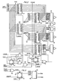
- Referring now to Figure 1,there is shown a functional block diagram of the instant invention. A
microprocessor 9 is provided with acontrol bus 10, an address bus 11 and adata bus 12. Thebus 10 is a 14-bit control bus, the bus 11 is a 16-bit address bus, and thebus 12 is an 8-bit bidirectional data bus. In this embodiment the busses are assumed to be associated with a Z80 microprocessor, although other microprocessors may be used instead. - The
minicomputer 16 is assumed to be of the Sperry Univac V70 series. Again, the invention may be used with other minicomputers. Theminicomputer 16 is connected to the upper and lower byte tri-statebusses control bus 15. The upper andlower byte busses microprocessor 9 produces an 8-bit data word and thecomputer 16 operates upon a 16-bit data word, with two bytes of data being required from themicroprocessor 9 to form an appropriate data word for thecomputer 16. - The
computer 16 is connected to thebus 15 by a suitable connectinglink 17 such as drivers or the like. Likewise, thebusses bus 15 byrespective driver networks - Upper and lower
byte data registers data bus 12 and to supply these 8-bit data words as the upper and lower bytes to thebusses control bus 10. - Upper and lower
byte address registers busses - A
map key register 22 is connected to receive mapping information from thedata bus 12 and to supply same to thecontrol bus 15 in order to control the mapping of the memory incomputer 16. A suitable register 25 (e.g., a FIFO memory) is connected to receive information from the bus 15 (16-bit words) and supply the information to bus 12 (two 8-bit bytes). Details of a suitable register are described in the co-pending European patent application by the present applicants, entitled Digital Information Transfer System and Interface (inventor: A.K. Fung). - In operation, the appropriate data bits are stored by the
microprocessor 9 viadata bus 12 in the upper and lowerbyte data registers registers microprocessor 9 via the bus 11. Also, themap key register 22 is set to the appropriate memory page by themicroprocessor 9 alongbus 12. When a "block move" instruction is executed by themicroprocessor 9, the information is externally transferred as described hereinafter. To themicroprocessor 9, the operation is equivalent to relocating data from one portion of the microprocessor memory to another portion thereof. However, the data is actually redirected from the microprocessor memory and transferred in a direct memory access operation to the memory of thecomputer 16. - Conversely, in a pre-fetch or DMA operation, data can be transferred directly from
computer 16 to the microprocessor viaregister 25. That is, the 16-bit word is applied to register 25 bybus 15. The information is then supplied tobus 12 as two 8-bit bytes and stored in the memory of the microprocessor. Such an operation is described in the co-pending patent European patent application referred to above. - Figure 2 shows a more detailed diagram of the circuitry of the instant invention. The upper and lower
byte data registers data bus 12. The inputs of themap key register 22 are also connected to thesame data bus 12. The address bus 11 is connected to the inputs of the upper and lowerbyte address registers byte data register 21 and the lowerbyte address register 24 are connected together and to thebus 14. Similarly, the output terminals of the upperbyte data register 20 and the upperbyte address register 23 are connected together and to thebus 13. The output terminals which form thebusses appropriate driver networks minicomputer bus 15, which is itself connected to theminicomputer 16 via thedriver network 17. - This circuit arrangement is necessary inasmuch as the
computer 16 is a 16-bit system while the microprocessor involved is an 8-bit system. The data bits DO through D7 are applied to both the upper and lowerbyte data registers data bus 12. The bits DO through D7 are selected by therespective registers byte data register 21 in which the bits are latched and stored. Subsequently, the next 8-bit byte is applied as data bit DO-D7 to the upperbyte data register 20 in which that information is then latched and stored. The output bits COBOO through COB07 are supplied from thelower byte register 21 to thebus 14 and then to thedriver circuit 18. Output bits COB08 through COB15 are supplied from theupper byte register 20 via thebus 13 to thedriver circuit 19. These signals are then supplied from thedriver circuits computer 16. - Likewise, the data bits DO through D7 are supplied to the
map key register 22 and, thence through thebus 15 to theminicomputer 16 as noted above. Themap key register 22 permits appropriate mapping arrangements so that a greater memory capacity can be utilized in the system. - In a similar manner, the upper and lower
byte address.registers byte address register 23 while the signals A01 through A08 are supplied to the lowerbyte address register 24. The output terminals of theregisters busses - In order to assure proper control, the data-ready (DRY) status is controlled by DRY circuitry (not shown) which in turn generates the trap data input signal (TPDI) which is supplied to enable terminals (OE) of
registers registers - Conversely, only during the function-ready (FRY) condition are the
address registers map register 22 enabled. The FRY condition, in turn, generates the trap address enable signal (TPADE) which is then supplied to the enable terminals (ØE) ofregisters busses - To control the clocking, and, thus, the loading of the data registers, a load control circuit is provided. This circuit includes a flip-
flop 37, and inverting ANDgates flop 37 is connected to receive the pull-up input signal PUP1. The initialization signal (INIT) is supplied to the pre-set (PRE) input terminal of flip-flop 37. With the application of this signal, flip-flop 37 is pre-set to the condition wherein the Q output terminal produces a high level signal and the Q terminal produces a low level signal. These signals are applied to one input terminal of each of the invertingNAND gates gates gates flop 37 are the inverse of one another. Therefore, with the application of the initialization signal INIT, thegates gates gate 36, theregister 20 is clocked, and latches and transfers the signals therein. At the same time, the LDCØB signal is supplied to the clock input terminal C of the flip-flop 37 and causes it to toggle. The signal levels at the Q and Q output terminals are switched and the states of thegates register 21 now becomes operative and theregister 20 is inoperative, being unable to receive and store signals. - The address bus, registers 23 and 24, are similarly activated by the application of the CØABST signal which is produced by an inverting NOR gate 41. One input terminal of the gate 41 is connected to the output terminal of an inverting AND
gate 38 which receives the trap transfer (TPXFR) signal from themicroprocessor 9 to indicate a DMA data transfer, and also the output signal fromgate 35. The trap transfer signal is used only when DMA data are to be transferred. - In the absence of the TPXFR signal, the
gate 38 does not produce an output signal for causing DMA operation and, therefore, no DMA address is entered into the address registers 23 and 24. In addition, the gate 41 receives an output signal from inverting ANDgate 39 which receives the pre-fetch input signal (PFFC) as well as the Q signal from a flip-flop 40 receives the PUP2 signal at its clear (CLR) input terminal. The C input terminal of the flip-flop 40 receives the TPXFR signal, while the D terminal receives the read/write command (CWR) signal which, during the initial DMA start-up cycle, activates thegate 39. With the pre-fetch signal (PFFC) present for the first DMA cycle, the first word will be fetched from the computer memory as described hereinafter. The pre-set terminal (PRE) of flip-flop 40 is connected to the output terminal ofgate 39 and the second input terminal gate 41. This has the effect of de-activating the latch flip-flop 40 after the first DMA cycle. - With the application of the TPXFR signal, the status of the
gate 38 and the δ output of the flip-flop 40 are controlled. In addition, the signal level at one input terminal of the gate 41 is established via thegate 38. With the operation- of the flip-flop 40, the status of thegate 39 is also controlled. With the application of the pre-fetch signal (PFFC), thegate 39 provides signals to the flip-flop 40 and the gate 41 which control the output signal which is produced by the gate 41 and supplied to theregisters - Figure 3 shows a detailed circuit diagram for the computer-oriented circuitry. In particular, Figure 3 shows the trap logic as well as the execute command and data output decode interfacing circuitry. In particular, an inverting NOR
gate 50 receives the TPDAE and the trap transfer (TPXFR) signals at its input terminals. These signals are supplied by the microprocessor and the computer control circuitry. Thegate 50 supplies a reset trap request output signal (RTRQ) to the pre-set terminal of a flip-flop 51. The CLR terminal of the flip-flop 51 receives the PUP1 signal referred to above. The D input terminal of flip-flop 51 is grounded, and the C input terminal receives the CØABST signal from the gate 41 of Figure 2. The Q output terminal of flip-flop 51 is left unconnected, while the Q output terminal is connected to supply the trap request TPRQ signal to one input terminal of thetrap logic circuit 52 which, together with the signal CWR, selects whether information is to be transferred to or fromcomputer 16 by means of the trap-in (TPIX) and the trap-out (TPOX) signals respectively. Thetrap logic circuit 52 is connected to receive the interrupt clock IUCX signal, in addition the command read/write signal (CWR), from a computer receiver interface circuitry (not shown). The IUCX signal is used to synchronize the data transfer with thebus 15. The output terminals oftrap logic circuit 52 produce the signal TPIX, which is supplied to thecomputer 16 when information data are to be transferred from themicroprocessor 9 to the computer, and the output signal TPOX, which is supplied to thecomputer 16 when data are to be transferred from the computer memory to the microprocessor. - Figure 4 shows a detailed circuit diagram of the microprocessor
bus control PROM 64 and the address decode logic used therewith. In particular,control logic circuit 62 receives control signals from the microprocessor I/O (input/output) port. Thecontrol logic circuit 62 supplies the data output signal (GØD) to the J terminal of flip-flop 63, and the block move control enable signal (BMCE) to the clock or toggle input terminal C of the flip-flop 63. The pre-set terminal receives the PUP1 signal while the clear (CLR) terminal receives the master reset signal (MRST). The Q output terminal of the flip-flop 63 is returned to the K input terminal thereof and, also, the terminal A4 of thebus control PROM 64. The A3 terminal of thePROM 64 receives the CWR signal while the A0 and A2 terminals receive the read (RD) and M1 signals, respectively. The write (WR) signal is supplied to terminal Al ofPROM 64. The output terminals of thePROM 64 are connected to produce, on terminals QO through Q3, the signals LDCØB, FØRM, PFFC and PMRQ respectively. The PFFC signal is the pre-fetch signal referred to above in connection with Figure 2. The LDCØB signal is supplied to thegates register 25 for transferring data and function signals from thecomputer 16 to themicroprocessor 9. The PMRQ signal is supplied to an input terminal of the microprocessor memory 65. - The PMRQ signal selectively enables or disables microprocessor memory 65 such that data is not returned to the local memory during a DMA transfer, or vice versa. That is, if the local memory is not disabled, the circuit acts as a "block-move" circuit and a block of data is relocated within the local memory. In this event, data is not transferred to the
computer 16. In addition, operation ofPROM 64 selectively causes the microprocessor to interface directly with the memory in the computer because the FORM signal enables appropriate tri-state drivers associated with theregister 25. - Table I below illustrates the basic operation of the
bus control PROM 64. ThePROM 64 receives five inputs and, thus, must operate on 32 possible combinations of signals. These combinations are numbered 0 (00000) to 31 (11111). These input signal combinations represent addresses for the PROM. The output signals represent the contents of the respective addresses which are listed. These output signals control the operation of the interfacing circuit. For example, thecombination number 17 has the address 10001 and the output 1100. This combination indicates that input signals BMMC and RD are binary ones and the other input signals are binary zeroes. The output signals PMRQ and PFFC are binary ones and the other output signals are binary zeroes. The input signals are assumed to be based on positive logic (i.e., 1 = true), while the output signals are based on negative logic (i.e., 1 = false). - More particularly, this condition indicates that
latch 63 has been set to select the phantom memory and the block move instruction (i.e., BMMC = 1). Also, the microprocessor has selected the read condition (i.e., RD = 1). Conversely, the write (WR), operation code fetch (Ml) and DMA transfer direction (CWR) are not selected (i.e., the microprocessor is not doing an operation code fetch, and the DMA transfer is from thecomputer 16 to the microprocessor 9). As a consequence, the contents of this PROM address, i.e. 1100, produce the signal (FORM) which enables theregister 25 for DMA transfer and at the same time the LOCOB triggers another DMA fetch cycle fromcomputer 16. Thus, the microprocessor memory can receive data from the computer memory. Also, in response to the PFFC = 1 signal, gate 41 is forced to produce the signal COABST which stores the address delivered by themicroprocessor 9 in address registers 23 and 24 and sets flip-flop 51 to placetrap logic circuit 52 in the TPØX state. With these conditions, thecomputer 16 can write data into theregister 25 for the next DMA operation. This completes the fetch cycle of the DMA operation. On the next microprocessor Z80 cycle, thePROM 64 address (10010) indicates the microprocessor is performing a write cycle (WR). The corresponding output 0111 of thePROM 64 makes PMRQ = 0, and this enables the microprocessor destination memory to receive the data fromregister 25 thus completing the store cycle of the DMA operation. It is clear, of course, that the microprocessor operation has not been particularly affected by the DMA operation. Data has been transferred directly from the computer memory to the microprocessor destination memory without requiring specifically dedicated microprocessor control signals. In short, during the fetch operation of the DMA cycle, themicroprocessor 9 performs a fetch cycle from its local memory, while the bus control PROM 65 enables .theregister 25, disables the local memory and places instead the data fromregister 25 ontobus 12 for the microprocessor to pick up. At the same time, the next DMA word is fetched from the memory ofminicomputer 16. During a store cycle, the microprocessor writes the data into the local memory to receive the data. It must be emphasised that the microprocessor only "knows" of and operates in its own memory space and its own domain. At no time does the microprocessor "realise" that a DMA operation is being performed between two separate systems. In this manner, software programs and hardware circuits can be designed in a simpler fashion. The same is true for the minicomputer. - Likewise, in the "pre-fetch" operation, data in a specified location in the computer is transferred to the microprocessor without requiring specifically dedicated microprocessor action. In this operation, the microprocessor supplies the signal 00001 (combination 2) to the
PROM 64 thereby indicating that a read (RD) operation is to occur. The PROM output signal 0011 enables the microprocessor memory 65 (PMRQ = 0), 0 and, also, thegate 39. As a result, the gate 41 produces the CØABST signal which sets the flip-flop 51 to produce the TPØX signal, and so cause thecomputer 16 to output data. In the meantime,computer 16 has made themicroprocessor 9 read an address which is coincident with the first DMA address in the minicomputer memory. The address and the corresponding contents are applied to thebusses registers register 25 from the computer memory. - In transferring data from the
microprocessor 9 to the computer 16 (combinations 25 and 26), a two-step operation is used. The input signal 11001 toPROM 64 produces the output signals 0111. The PMRQ = 0 signal enables the microprocessor memory 65 which then permits the selected data to be placed onbus 12. Thereafter, the input signal 11010 produces thePROM 64 output signals 1110. The LDCØB = 0 signal causes registers 20 or 21 to be loaded in accordance with the description above. - Thus, the
microprocessor 9 operates without special instructions from the computer and vice versa. Rather, information is merely "dumped onto the busses" and selectively directed in accordance with the operation of the interface circuitry as controlled by thePROM 64.
- Thus, there is shown and described a circuit which permits direct memory accessing (DMA) between a microprocessor and a computer memory. That is, information in the memory of the microprocessor is placed on the
busses 11 and 12 of the microprocessor undercontrol 16, and in response to, signals within the microprocessor. Depending upon other control signals which are supplied to thebus control PROM 64 and thelatch 63, the information is transferred to thecomputer 16 via the interfacing network. That is, data is transferred to the appropriate registers (20, 21) for transfer to the computer. The address for the data is also transferred by appropriate registers (23, 24) to the computer in a similar fashion. The mapkey register 22 selects that portion of the computer memory to which the data is to be transferred. The microprocessor is an 8-bit machine or system, while the computer is a 16-bit machine or system. Consequently, data to be supplied to the computer has to be provided by the microprocessor in two 8- bit bytes. These bytes are identified as the upper and lower bytes. - In this embodiment, the addresses of the bytes are also transferred in 8-bit bytes to be utilized in the 16-bit machine. However, in order to expedite the transfer and to reduce the number of components which are required, the address information, which is to be transferred to the computer, is shifted by one bit on input into the address registers 23 and 24. For example, register 24 receives the address bits A01 through A08. These bits are supplied to the computer bus as the computer address bits CØB00 through COB07. Similarly, address bits A09-A15 are transferred via
register 23. The shifting of addresses A00-A15 has the effect of reducing the addresses supplied to the computer by one-half, or, in other words, packing two 8-bit .data bytes into one 16-bit word. - By referring to Table II is seen that the omission or dropping of the least significant bit (A00) in the address registers has the effect of transferring two consecutive data bytes into the same address in the computer memory. This circuit arrangement effects a substantial saving in the circuitry components required to transfer the data from the microprocessor to the computer.

- The foregoing description of an embodiment, illustrates how a DMA operation is effected between a microprocessor and a computer. Use is made of the existing firmware, i.e., the "block data move" instruction in the microprocessor. It permits a DMA operation to be effected through standard registers. It also permits the data transfer to be effected externally, i.e. from memory-to-memory across a boundary between two separate systems or machines. In effect, the microprocessor operates in such a fashion that the computer memory appears to be a part of the microprocessor memory, and whenever a block data move or manipulation is completed within the microprocessor, the DMA operation is also completed vis-a-vis the computer. This operation, as performed by the present invention, permits the transfer of data provided the requisite address and data identifications are available in the microprocessor. It must be recognized that the microprocessor does not actively "transfer" data to the computer. Instead, the microprocessor places data onto a data bus as if for an internal operation. However, other logic signals are supplied to a PROM which effectively diverts the data from the bus to an interfacing circuit and, thence, to the computer. The computer, likewise, places data on to the microprocessor data bus via interfacing circuitry. As a result, the circuitry in the computer and microprocessor are altered in only insignificant ways but the very powerful data transfer capability is obtained.
Claims (9)
Applications Claiming Priority (2)
| Application Number | Priority Date | Filing Date | Title |
|---|---|---|---|
| US06/079,209 US4344130A (en) | 1979-09-26 | 1979-09-26 | Apparatus to execute DMA transfer between computing devices using a block move instruction |
| US79209 | 1979-09-26 |
Publications (3)
| Publication Number | Publication Date |
|---|---|
| EP0026648A2 true EP0026648A2 (en) | 1981-04-08 |
| EP0026648A3 EP0026648A3 (en) | 1981-04-22 |
| EP0026648B1 EP0026648B1 (en) | 1986-08-13 |
Family
ID=22149111
Family Applications (1)
| Application Number | Title | Priority Date | Filing Date |
|---|---|---|---|
| EP80303386A Expired EP0026648B1 (en) | 1979-09-26 | 1980-09-26 | Digital data transfer apparatus |
Country Status (5)
| Country | Link |
|---|---|
| US (1) | US4344130A (en) |
| EP (1) | EP0026648B1 (en) |
| JP (1) | JPS6016998Y2 (en) |
| CA (1) | CA1143850A (en) |
| DE (1) | DE3071698D1 (en) |
Cited By (4)
| Publication number | Priority date | Publication date | Assignee | Title |
|---|---|---|---|---|
| FR2526561A1 (en) * | 1982-05-10 | 1983-11-10 | Sony Corp | MICROPROCESSOR MICROCOMPUTER SYSTEM |
| EP0207472A2 (en) * | 1985-07-01 | 1987-01-07 | Honeywell Inc. | Microprocessor assisted data block transfer apparatus |
| EP0212152A2 (en) * | 1985-07-01 | 1987-03-04 | Honeywell Inc. | Microprocessor assisted memory to memory move apparatus |
| EP0321157A2 (en) * | 1987-12-15 | 1989-06-21 | Advanced Micro Devices, Inc. | Direct memory access apparatus and methods |
Families Citing this family (9)
| Publication number | Priority date | Publication date | Assignee | Title |
|---|---|---|---|---|
| US4538224A (en) * | 1982-09-30 | 1985-08-27 | At&T Bell Laboratories | Direct memory access peripheral unit controller |
| US5208915A (en) * | 1982-11-09 | 1993-05-04 | Siemens Aktiengesellschaft | Apparatus for the microprogram control of information transfer and a method for operating the same |
| JPH0644245B2 (en) * | 1983-12-29 | 1994-06-08 | 富士通株式会社 | Store buffer device |
| US4779190A (en) * | 1986-12-03 | 1988-10-18 | Ncr Corporation | Communication bus interface |
| JP3005626B2 (en) * | 1988-09-21 | 2000-01-31 | 株式会社日立製作所 | Data processing system and data transfer method |
| EP0408810B1 (en) * | 1989-07-20 | 1996-03-20 | Kabushiki Kaisha Toshiba | Multi processor computer system |
| JP3190032B2 (en) * | 1990-06-12 | 2001-07-16 | 株式会社東芝 | Data storage device |
| US5671443A (en) * | 1995-02-21 | 1997-09-23 | International Business Machines Corporation | Direct memory access acceleration device for use in a data processing system |
| US6212601B1 (en) * | 1996-08-30 | 2001-04-03 | Texas Instruments Incorporated | Microprocessor system with block move circuit disposed between cache circuits |
Citations (2)
| Publication number | Priority date | Publication date | Assignee | Title |
|---|---|---|---|---|
| FR2235427A1 (en) * | 1973-06-28 | 1975-01-24 | Ibm | Connecting cct. for satellite data processors - has minimum number of programme interruptions in main processor |
| US4159532A (en) * | 1977-08-04 | 1979-06-26 | Honeywell Information Systems Inc. | FIFO look-ahead system |
Family Cites Families (11)
| Publication number | Priority date | Publication date | Assignee | Title |
|---|---|---|---|---|
| US3932841A (en) * | 1973-10-26 | 1976-01-13 | Raytheon Company | Bus controller for digital computer system |
| US3940743A (en) * | 1973-11-05 | 1976-02-24 | Digital Equipment Corporation | Interconnecting unit for independently operable data processing systems |
| GB1474385A (en) * | 1973-12-14 | 1977-05-25 | Int Computers Ltd | Multiprocessor data processing systems |
| US4130865A (en) * | 1974-06-05 | 1978-12-19 | Bolt Beranek And Newman Inc. | Multiprocessor computer apparatus employing distributed communications paths and a passive task register |
| US3969704A (en) * | 1974-07-19 | 1976-07-13 | Nanodata Corporation | Word transformation apparatus for digital information processing |
| GB1505535A (en) * | 1974-10-30 | 1978-03-30 | Motorola Inc | Microprocessor system |
| US4050096A (en) * | 1974-10-30 | 1977-09-20 | Motorola, Inc. | Pulse expanding system for microprocessor systems with slow memory |
| US4124888A (en) * | 1975-12-24 | 1978-11-07 | Computer Automation, Inc. | Peripheral-unit controller apparatus |
| US4112490A (en) * | 1976-11-24 | 1978-09-05 | Intel Corporation | Data transfer control apparatus and method |
| US4099236A (en) * | 1977-05-20 | 1978-07-04 | Intel Corporation | Slave microprocessor for operation with a master microprocessor and a direct memory access controller |
| US4128883A (en) * | 1977-09-30 | 1978-12-05 | Ncr Corporation | Shared busy means in a common bus environment |
-
1979
- 1979-09-26 US US06/079,209 patent/US4344130A/en not_active Expired - Lifetime
-
1980
- 1980-07-30 CA CA000357318A patent/CA1143850A/en not_active Expired
- 1980-09-26 EP EP80303386A patent/EP0026648B1/en not_active Expired
- 1980-09-26 DE DE8080303386T patent/DE3071698D1/en not_active Expired
- 1980-09-26 JP JP1980137042U patent/JPS6016998Y2/en not_active Expired
Patent Citations (2)
| Publication number | Priority date | Publication date | Assignee | Title |
|---|---|---|---|---|
| FR2235427A1 (en) * | 1973-06-28 | 1975-01-24 | Ibm | Connecting cct. for satellite data processors - has minimum number of programme interruptions in main processor |
| US4159532A (en) * | 1977-08-04 | 1979-06-26 | Honeywell Information Systems Inc. | FIFO look-ahead system |
Non-Patent Citations (7)
| Title |
|---|
| Computer, vol. 10, no. 5, May 1977 pp. 68-74 3rd Euromicro Symposium, Amsterdam, 1977, pp. 16-22 * |
| NACHRICHTENTECHNIKELEKTRONIK, Vol. 29, No. 6, June 1979, Berlin, DE, CIMANDER et al.: "Mehrmikrorechnersysteme mit Registerkopplung", pages 229-232 * |
| PROCEEDING OF THE NATIONAL ELECTRONICS CONFERENCE, Vol. 32, 16-18- Oct. 1978, Oak Brook, Illinois, US MITTON et al.: "Microprocessor based communications interfaces", pages 61-63 * |
| PROCEEDINGS OF THE COMPCON, conference on 4-7 September 1979 in Washington; Proceedings printed in New York, US BUSTOS et al.: "A parallel array of microprcessors- an alternative solution to diffusion problems", pages 380-389 * |
| PROCEEDINGS OF THE COMPCON; conference on 4-7 September 1979 in Washington; Proceedings printed in New York, US PEARSE O'GRADY: "Interprocessor communication in multiprocessor simulation systems", pages 300-306. * |
| PROCEEDINGS OF THE NATIONAL ELECTRONICS CONFERENCE, vol. 32, 16-18- Oct. 1978, Oak Brook, Illinois, US MITTON et al.: "Microprocessor based communications interfaces", pages 61-63. * |
| PROEEDINGS OF THE COMPCON; conference on 4-7 September 1979 in Washington; Proceedings printed in New York, US PEARSE O'GRADY: "Interprocessor communication in multiprocessor simulation systems", pages 300-306 * |
Cited By (8)
| Publication number | Priority date | Publication date | Assignee | Title |
|---|---|---|---|---|
| FR2526561A1 (en) * | 1982-05-10 | 1983-11-10 | Sony Corp | MICROPROCESSOR MICROCOMPUTER SYSTEM |
| GB2119977A (en) * | 1982-05-10 | 1983-11-23 | Sony Corp | Microcomputer systems |
| EP0207472A2 (en) * | 1985-07-01 | 1987-01-07 | Honeywell Inc. | Microprocessor assisted data block transfer apparatus |
| EP0212152A2 (en) * | 1985-07-01 | 1987-03-04 | Honeywell Inc. | Microprocessor assisted memory to memory move apparatus |
| EP0212152A3 (en) * | 1985-07-01 | 1988-08-24 | Honeywell Inc. | Microprocessor assisted memory to memory move apparatus |
| EP0207472A3 (en) * | 1985-07-01 | 1988-08-31 | Honeywell Inc. | Microprocessor assisted data block transfer apparatus |
| EP0321157A2 (en) * | 1987-12-15 | 1989-06-21 | Advanced Micro Devices, Inc. | Direct memory access apparatus and methods |
| EP0321157A3 (en) * | 1987-12-15 | 1991-03-20 | Advanced Micro Devices, Inc. | Direct memory access apparatus and methods |
Also Published As
| Publication number | Publication date |
|---|---|
| DE3071698D1 (en) | 1986-09-18 |
| EP0026648B1 (en) | 1986-08-13 |
| JPS5649934U (en) | 1981-05-02 |
| EP0026648A3 (en) | 1981-04-22 |
| CA1143850A (en) | 1983-03-29 |
| US4344130A (en) | 1982-08-10 |
| JPS6016998Y2 (en) | 1985-05-25 |
Similar Documents
| Publication | Publication Date | Title |
|---|---|---|
| US4271466A (en) | Direct memory access control system with byte/word control of data bus | |
| US4447878A (en) | Apparatus and method for providing byte and word compatible information transfers | |
| US5642489A (en) | Bridge between two buses of a computer system with a direct memory access controller with accessible registers to support power management | |
| US5860021A (en) | Single chip microcontroller having down-loadable memory organization supporting "shadow" personality, optimized for bi-directional data transfers over a communication channel | |
| US4467447A (en) | Information transferring apparatus | |
| KR950004453B1 (en) | Register circuit having the function of inter-register copying | |
| US4458313A (en) | Memory access control system | |
| EP0218523B1 (en) | programmable access memory | |
| US6216191B1 (en) | Field programmable gate array having a dedicated processor interface | |
| US5109333A (en) | Data transfer control method and apparatus for co-processor system | |
| JPS6259822B2 (en) | ||
| EP0026648A2 (en) | Digital data transfer apparatus | |
| US5175831A (en) | System register initialization technique employing a non-volatile/read only memory | |
| KR19980069757A (en) | Microprocessor and Multiprocessor Systems | |
| US6173383B1 (en) | Interface bridge between a system bus and local buses with translation of local addresses for system space access programmable by address space | |
| US4764896A (en) | Microprocessor assisted memory to memory move apparatus | |
| US3673575A (en) | Microprogrammed common control unit with double format control words | |
| EP0337537A1 (en) | Computer system comprising a main bus and an additional communication line directly connected between processor and main memory | |
| US4628450A (en) | Data processing system having a local memory which does not use a directory device with distributed resident programs and a method therefor | |
| KR970059914A (en) | Flash memory system | |
| KR100261154B1 (en) | Dma controller | |
| JPH0227696B2 (en) | JOHOSHORISOCHI | |
| JPS58201157A (en) | Control circuit of bank memory | |
| JPH05120207A (en) | Data transfer system | |
| KR900009212Y1 (en) | Address control apparatus |
Legal Events
| Date | Code | Title | Description |
|---|---|---|---|
| PUAI | Public reference made under article 153(3) epc to a published international application that has entered the european phase |
Free format text: ORIGINAL CODE: 0009012 |
|
| PUAL | Search report despatched |
Free format text: ORIGINAL CODE: 0009013 |
|
| AK | Designated contracting states |
Designated state(s): DE FR GB IT SE |
|
| AK | Designated contracting states |
Designated state(s): DE FR GB IT SE |
|
| 17P | Request for examination filed |
Effective date: 19810904 |
|
| GRAA | (expected) grant |
Free format text: ORIGINAL CODE: 0009210 |
|
| AK | Designated contracting states |
Kind code of ref document: B1 Designated state(s): DE FR GB IT SE |
|
| ITF | It: translation for a ep patent filed | ||
| REF | Corresponds to: |
Ref document number: 3071698 Country of ref document: DE Date of ref document: 19860918 |
|
| ET | Fr: translation filed | ||
| PLBE | No opposition filed within time limit |
Free format text: ORIGINAL CODE: 0009261 |
|
| STAA | Information on the status of an ep patent application or granted ep patent |
Free format text: STATUS: NO OPPOSITION FILED WITHIN TIME LIMIT |
|
| 26N | No opposition filed | ||
| PGFP | Annual fee paid to national office [announced via postgrant information from national office to epo] |
Ref country code: SE Payment date: 19920811 Year of fee payment: 13 |
|
| ITTA | It: last paid annual fee | ||
| PG25 | Lapsed in a contracting state [announced via postgrant information from national office to epo] |
Ref country code: SE Effective date: 19930927 |
|
| PGFP | Annual fee paid to national office [announced via postgrant information from national office to epo] |
Ref country code: DE Payment date: 19940929 Year of fee payment: 15 |
|
| EUG | Se: european patent has lapsed |
Ref document number: 80303386.9 Effective date: 19940410 |
|
| PGFP | Annual fee paid to national office [announced via postgrant information from national office to epo] |
Ref country code: FR Payment date: 19950908 Year of fee payment: 16 |
|
| PG25 | Lapsed in a contracting state [announced via postgrant information from national office to epo] |
Ref country code: DE Effective date: 19960601 |
|
| PG25 | Lapsed in a contracting state [announced via postgrant information from national office to epo] |
Ref country code: FR Effective date: 19960930 |
|
| REG | Reference to a national code |
Ref country code: FR Ref legal event code: ST |
|
| REG | Reference to a national code |
Ref country code: FR Ref legal event code: ST |
|
| PGFP | Annual fee paid to national office [announced via postgrant information from national office to epo] |
Ref country code: GB Payment date: 19980806 Year of fee payment: 19 |
|
| PG25 | Lapsed in a contracting state [announced via postgrant information from national office to epo] |
Ref country code: GB Free format text: LAPSE BECAUSE OF NON-PAYMENT OF DUE FEES Effective date: 19990926 |
|
| GBPC | Gb: european patent ceased through non-payment of renewal fee |
Effective date: 19990926 |