EP0205385B1 - Verfahren zur Herstellung einer Platte zum Aufbau von abnehmbaren Schaltungen, insbesondere für ein pädagogisches Spiel - Google Patents
Verfahren zur Herstellung einer Platte zum Aufbau von abnehmbaren Schaltungen, insbesondere für ein pädagogisches Spiel Download PDFInfo
- Publication number
- EP0205385B1 EP0205385B1 EP86401236A EP86401236A EP0205385B1 EP 0205385 B1 EP0205385 B1 EP 0205385B1 EP 86401236 A EP86401236 A EP 86401236A EP 86401236 A EP86401236 A EP 86401236A EP 0205385 B1 EP0205385 B1 EP 0205385B1
- Authority
- EP
- European Patent Office
- Prior art keywords
- hairs
- tufts
- support
- holes
- hole
- Prior art date
- Legal status (The legal status is an assumption and is not a legal conclusion. Google has not performed a legal analysis and makes no representation as to the accuracy of the status listed.)
- Expired
Links
Images
Classifications
-
- H—ELECTRICITY
- H05—ELECTRIC TECHNIQUES NOT OTHERWISE PROVIDED FOR
- H05K—PRINTED CIRCUITS; CASINGS OR CONSTRUCTIONAL DETAILS OF ELECTRIC APPARATUS; MANUFACTURE OF ASSEMBLAGES OF ELECTRICAL COMPONENTS
- H05K3/00—Apparatus or processes for manufacturing printed circuits
- H05K3/30—Assembling printed circuits with electric components, e.g. with resistors
- H05K3/32—Assembling printed circuits with electric components, e.g. with resistors electrically connecting electric components or wires to printed circuits
- H05K3/325—Assembling printed circuits with electric components, e.g. with resistors electrically connecting electric components or wires to printed circuits by abutting or pinching; Mechanical auxiliary parts therefor
- H05K3/326—Assembling printed circuits with electric components, e.g. with resistors electrically connecting electric components or wires to printed circuits by abutting or pinching; Mechanical auxiliary parts therefor the printed circuit having integral resilient or deformable parts, e.g. tabs or parts of flexible circuits
-
- H—ELECTRICITY
- H05—ELECTRIC TECHNIQUES NOT OTHERWISE PROVIDED FOR
- H05K—PRINTED CIRCUITS; CASINGS OR CONSTRUCTIONAL DETAILS OF ELECTRIC APPARATUS; MANUFACTURE OF ASSEMBLAGES OF ELECTRICAL COMPONENTS
- H05K7/00—Constructional details common to different types of electric apparatus
- H05K7/02—Arrangements of circuit components or wiring on supporting structure
- H05K7/06—Arrangements of circuit components or wiring on supporting structure on insulating boards, e.g. wiring harnesses
- H05K7/08—Arrangements of circuit components or wiring on supporting structure on insulating boards, e.g. wiring harnesses on perforated boards
-
- Y—GENERAL TAGGING OF NEW TECHNOLOGICAL DEVELOPMENTS; GENERAL TAGGING OF CROSS-SECTIONAL TECHNOLOGIES SPANNING OVER SEVERAL SECTIONS OF THE IPC; TECHNICAL SUBJECTS COVERED BY FORMER USPC CROSS-REFERENCE ART COLLECTIONS [XRACs] AND DIGESTS
- Y10—TECHNICAL SUBJECTS COVERED BY FORMER USPC
- Y10S—TECHNICAL SUBJECTS COVERED BY FORMER USPC CROSS-REFERENCE ART COLLECTIONS [XRACs] AND DIGESTS
- Y10S439/00—Electrical connectors
- Y10S439/93—Coupling part wherein contact is comprised of a wire or brush
-
- Y—GENERAL TAGGING OF NEW TECHNOLOGICAL DEVELOPMENTS; GENERAL TAGGING OF CROSS-SECTIONAL TECHNOLOGIES SPANNING OVER SEVERAL SECTIONS OF THE IPC; TECHNICAL SUBJECTS COVERED BY FORMER USPC CROSS-REFERENCE ART COLLECTIONS [XRACs] AND DIGESTS
- Y10—TECHNICAL SUBJECTS COVERED BY FORMER USPC
- Y10T—TECHNICAL SUBJECTS COVERED BY FORMER US CLASSIFICATION
- Y10T29/00—Metal working
- Y10T29/49—Method of mechanical manufacture
- Y10T29/49002—Electrical device making
- Y10T29/49117—Conductor or circuit manufacturing
- Y10T29/49124—On flat or curved insulated base, e.g., printed circuit, etc.
- Y10T29/4913—Assembling to base an electrical component, e.g., capacitor, etc.
- Y10T29/49139—Assembling to base an electrical component, e.g., capacitor, etc. by inserting component lead or terminal into base aperture
Definitions
- the present invention relates to a method of manufacturing a mounting panel for removable elements, in particular for educational toys for performing simple electronic assemblies "in the air", of the "Eiffel Tower” assembly type.
- an insulating material support is used on which conductive contact points are arranged, or an insulating material support pierced with holes in which plugs of flexible conductive material are molded as described in the patent.
- Mounting panels of the type under consideration consist of contact springs mounted between an upper plate and a lower plate, and accessible, for connection, by holes drilled in the upper plate.
- Another known mounting panel is constituted, as described in patent FR-A-2 446 544, by an annular groove offering an internal wall and an external wall and by an elastic element disposed in the annular groove, it being understood that the internal and external walls can be electrically conductive and the insulating elastic element or vice versa.
- connection panel made of insulating material, pierced with holes opening into one of its faces and into which bundles of parallel conductive wires are engaged. extending flush with the face of the panel.
- the internal ends of the wires of the same package are embedded in a base of conductive material to which is connected an electrical conductor usually produced in the form of a printed circuit trace.
- a mounting panel of the aforementioned type is obviously difficult to manufacture, requiring the use of several machines and therefore it is costly.
- the present invention aims to remedy these drawbacks by providing a particularly simple manufacturing means, which results in a relatively low cost price.
- this kind of mounting panel makes it possible to maintain good contact after numerous manipulations.
- this method of manufacturing a panel for mounting removable elements making it possible to carry out simple electronic assemblies "in the air” of the "Eiffel Tower” type, from components.
- elementary comprising a support pierced with holes opening into at least one face of the support and respectively containing tufts of bristles parallel to each other thus constituting studs which can be used to longitudinally drive in the branches of the components to be mounted on the panel, is characterized in that the tufts of parallel bristles are engaged in the respective holes of the support, leaving part of the bristles to extend outside like the bristles of a brush, and the tufts of bristles are then cut with flush with the face of the support into which the holes open.
- the bristles used to form the "studs” may be metallic or made of an electrically conductive material or else of insulating material when the function of electrical connection must not be assumed.
- the “studs” can advantageously be constituted by tufts of bristles stuffed in the holes so that each bristle forms a sort of U in the hole, the U bristles of each tuft being fixed in the hole by means of a point or clip driven into the bottom of the hole.
- the holes drilled in the mounting panel to accommodate the tufts of bristles can be blind holes or else they can pass through the panel right through.
- the bristles constituting the studs are strands wavy in the longitudinal direction.
- the applications of the mounting panel according to the invention are numerous and varied. We can cite, for example, simple electronic assemblies “in the air” of the “Eiffel Tower” type, or even creations based on wire (or other material) using the same technique as the connection wires of electronic components, for example the presentation of objects on a wire cradle, threadlike figures, etc.
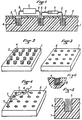
- FIG. 1 represents a mounting panel supporting two electronic components and which essentially consists of a support 1 made of electrically insulating material covered or not by a cover 2 made of plastic material.
- the insulating support is pierced with holes 3, preferably blind, which open into its upper face.
- holes 3 preferably blind, which open into its upper face.
- the connecting wires 6, coming from the components 7, can have the same diameter or different diameters. In all cases, the electrical connection between two connecting wires engaged in the same stud 5 is ensured under the best conditions, due to the relative transverse elasticity of the bristles of each tuft 4.
- the method of manufacturing the panel according to the invention consists of an insulating plate constituting the insulating support 1, to be drilled in this plate. that the holes 3 and to engage in each hole a tuft of bristles 4 extending out of the hole (FIG. 2) as the bristles of a brush are fixed in a support, for example made of wood.
- FIG. 4 In the embodiment of the invention shown in Figure 4 is shown an application of the mounting panel according to the invention.
- the tufts of bristles 4 forming the studs 5 are formed by wavy strands.
- the studs 5 can advantageously be constituted by tufts of bristles stuffed in the holes 3 so that each bristle 4 forms a sort of U in the hole, the bristles in U of each tuft being fixed in the hole by means of a point or clip 8 pressed into the bottom of the hole.
Landscapes
- Engineering & Computer Science (AREA)
- Microelectronics & Electronic Packaging (AREA)
- Metallurgy (AREA)
- Manufacturing & Machinery (AREA)
- Toys (AREA)
- Elimination Of Static Electricity (AREA)
- Pinball Game Machines (AREA)
- Application Of Or Painting With Fluid Materials (AREA)
- Finishing Walls (AREA)
Claims (3)
Priority Applications (1)
| Application Number | Priority Date | Filing Date | Title |
|---|---|---|---|
| AT86401236T ATE48930T1 (de) | 1985-06-10 | 1986-06-09 | Verfahren zur herstellung einer platte zum aufbau von abnehmbaren schaltungen, insbesondere fuer ein paedagogisches spiel. |
Applications Claiming Priority (2)
| Application Number | Priority Date | Filing Date | Title |
|---|---|---|---|
| FR8508732 | 1985-06-10 | ||
| FR8508732A FR2583254A1 (fr) | 1985-06-10 | 1985-06-10 | Panneau de montage d'elements amovibles, en particulier pour jouets pedagogiques |
Publications (2)
| Publication Number | Publication Date |
|---|---|
| EP0205385A1 EP0205385A1 (de) | 1986-12-17 |
| EP0205385B1 true EP0205385B1 (de) | 1989-12-20 |
Family
ID=9320047
Family Applications (1)
| Application Number | Title | Priority Date | Filing Date |
|---|---|---|---|
| EP86401236A Expired EP0205385B1 (de) | 1985-06-10 | 1986-06-09 | Verfahren zur Herstellung einer Platte zum Aufbau von abnehmbaren Schaltungen, insbesondere für ein pädagogisches Spiel |
Country Status (5)
| Country | Link |
|---|---|
| US (1) | US4746300A (de) |
| EP (1) | EP0205385B1 (de) |
| AT (1) | ATE48930T1 (de) |
| DE (1) | DE3667744D1 (de) |
| FR (1) | FR2583254A1 (de) |
Families Citing this family (18)
| Publication number | Priority date | Publication date | Assignee | Title |
|---|---|---|---|---|
| US5917707A (en) | 1993-11-16 | 1999-06-29 | Formfactor, Inc. | Flexible contact structure with an electrically conductive shell |
| US4955523A (en) * | 1986-12-17 | 1990-09-11 | Raychem Corporation | Interconnection of electronic components |
| US5189507A (en) * | 1986-12-17 | 1993-02-23 | Raychem Corporation | Interconnection of electronic components |
| FR2637154B1 (fr) * | 1988-09-26 | 1994-06-24 | Ducroux Maurice | Panneau de montage d'elements amovibles notamment pour des montages electriques ou electroniques |
| FR2712135B1 (fr) * | 1993-11-05 | 1996-01-19 | Le Strat Guy | Dispositif d'assemblage et d'interconnexion de composants pour la réalisation de circuits électroniques et câblage de circuit électronique. |
| US20020053734A1 (en) | 1993-11-16 | 2002-05-09 | Formfactor, Inc. | Probe card assembly and kit, and methods of making same |
| US5820014A (en) | 1993-11-16 | 1998-10-13 | Form Factor, Inc. | Solder preforms |
| US7073254B2 (en) | 1993-11-16 | 2006-07-11 | Formfactor, Inc. | Method for mounting a plurality of spring contact elements |
| US5994152A (en) | 1996-02-21 | 1999-11-30 | Formfactor, Inc. | Fabricating interconnects and tips using sacrificial substrates |
| US8033838B2 (en) | 1996-02-21 | 2011-10-11 | Formfactor, Inc. | Microelectronic contact structure |
| US6617522B2 (en) * | 2001-05-30 | 2003-09-09 | Nokia Corporation | Connector apparatus, and associated method, formed of material exhibiting physical-memory characteristics |
| US20040163717A1 (en) * | 2003-02-21 | 2004-08-26 | Cookson Electronics, Inc. | MEMS device assembly |
| US20050012212A1 (en) * | 2003-07-17 | 2005-01-20 | Cookson Electronics, Inc. | Reconnectable chip interface and chip package |
| US6881074B1 (en) * | 2003-09-29 | 2005-04-19 | Cookson Electronics, Inc. | Electrical circuit assembly with micro-socket |
| DE102006046471A1 (de) * | 2006-04-11 | 2007-10-18 | Robert Bosch Gmbh | Werkzeuglos herstell- und lösbare elektrische Verbindung |
| ATE528222T1 (de) * | 2007-08-29 | 2011-10-15 | Graphic Packaging Int Inc | Verbindungsbehältersystem für lebensmittel oder andere produkte |
| US7614907B2 (en) * | 2008-02-12 | 2009-11-10 | Chaojiong Zhang | Contact terminal with self-adjusting contact surface |
| DE102009020984A1 (de) * | 2008-05-13 | 2009-11-19 | Continental Teves Ag & Co. Ohg | Toleranzausgleichender elektrischer Verbinder, insbesondere für Kraftfahrzeugsteuergeräte |
Family Cites Families (8)
| Publication number | Priority date | Publication date | Assignee | Title |
|---|---|---|---|---|
| GB1387587A (en) * | 1971-07-22 | 1975-03-19 | Plessey Co Ltd | Electrical interconnectors and connector assemblies |
| US3982320A (en) * | 1975-02-05 | 1976-09-28 | Technical Wire Products, Inc. | Method of making electrically conductive connector |
| JPS5273392A (en) * | 1975-12-17 | 1977-06-20 | Fujitsu Ltd | Connector |
| DE2743877A1 (de) * | 1977-09-29 | 1979-04-12 | Siemens Ag | Elektrisches kontaktelement |
| DE2804587A1 (de) * | 1978-02-03 | 1979-08-09 | Peter Kammermeier | Grundplatte zum loetlosen aufbau elektrischer und/oder elektronischer schaltungen |
| JPS56117476U (de) * | 1980-02-09 | 1981-09-08 | ||
| DE3265993D1 (en) * | 1981-06-30 | 1985-10-10 | Ibm | Electric circuit connecting devices |
| AU8205282A (en) * | 1982-03-17 | 1983-10-24 | Charvolin Patrice | Kit for making electric circuits |
-
1985
- 1985-06-10 FR FR8508732A patent/FR2583254A1/fr active Pending
-
1986
- 1986-06-09 EP EP86401236A patent/EP0205385B1/de not_active Expired
- 1986-06-09 DE DE8686401236T patent/DE3667744D1/de not_active Expired - Fee Related
- 1986-06-09 AT AT86401236T patent/ATE48930T1/de not_active IP Right Cessation
- 1986-12-03 US US06/937,310 patent/US4746300A/en not_active Expired - Fee Related
Also Published As
| Publication number | Publication date |
|---|---|
| ATE48930T1 (de) | 1990-01-15 |
| DE3667744D1 (de) | 1990-01-25 |
| EP0205385A1 (de) | 1986-12-17 |
| FR2583254A1 (fr) | 1986-12-12 |
| US4746300A (en) | 1988-05-24 |
Similar Documents
| Publication | Publication Date | Title |
|---|---|---|
| EP0205385B1 (de) | Verfahren zur Herstellung einer Platte zum Aufbau von abnehmbaren Schaltungen, insbesondere für ein pädagogisches Spiel | |
| CA1311724C (fr) | Brosse pour l'application de produits cosmetiques, en particulier de mascara | |
| JP5005982B2 (ja) | 化粧物質を塗布するためのブラシ | |
| EP0329505B1 (de) | Bürste zum Applizieren von Schminke und Behälter und Produkt ausgerüstet mit einer solchen Bürste | |
| KR101004783B1 (ko) | 칫솔 및 그 칫솔의 제조 방법 | |
| EP1155637B1 (de) | Auftragevorrichtung mit unverdrilltem Kern | |
| EP1302128B1 (de) | Applikator für kosmetische Produkte, insbesondere auf Wimpern oder Augenbrauen | |
| US5584567A (en) | Decorative light mount | |
| FR2958130A1 (fr) | Applicateur pour appliquer un produit sur les cils et/ou sourcils. | |
| US20100083979A1 (en) | Mascara brush | |
| FR2916328A1 (fr) | Brosse pour l'application d'un produit sur les cils et/ou les sourcils | |
| FR2488059A1 (fr) | Connecteur electrique destine a etre dispose a l'extremite d'un cable electrique plat a plusieurs conducteurs | |
| FR2578361A1 (fr) | Distributeur electrique de forme modulaire, destine en particulier aux applications aeronautiques et aerospatiales | |
| FR2743704A3 (fr) | Brosse a dents avec touffes de poils mobiles | |
| FR2494504A1 (fr) | Connecteur a sertir pour fils electriques | |
| EP2555652A1 (de) | Doppelapplikator zum auftragen eines produkts auf die wimpern | |
| FR2566969A1 (fr) | Element de contact electrique d'un connecteur et procede de fabrication de cet element | |
| FR2663826A1 (fr) | Brosse pour appliquer du mascara sur les cils, et procede de fabrication d'une telle brosse. | |
| FR2493132A1 (fr) | Porte-brosses pour appareils electriques a brosser les tapis | |
| WO2006029008B1 (en) | Resilient pipeline inspection brush | |
| CA2300665A1 (en) | Applicator brush | |
| EP1111733B1 (de) | Flexible Verbindungsanordnung | |
| JP3120887U (ja) | 静電気除去ブラシ | |
| FR2872006A1 (fr) | Brosse de maquillage a courbure variable | |
| WO1998010681A1 (fr) | Brosse a mascara perfectionnee |
Legal Events
| Date | Code | Title | Description |
|---|---|---|---|
| PUAI | Public reference made under article 153(3) epc to a published international application that has entered the european phase |
Free format text: ORIGINAL CODE: 0009012 |
|
| AK | Designated contracting states |
Kind code of ref document: A1 Designated state(s): AT BE CH DE FR GB IT LI LU NL SE |
|
| 17P | Request for examination filed |
Effective date: 19870519 |
|
| RIN1 | Information on inventor provided before grant (corrected) |
Inventor name: DUCROUX, MAURICE Inventor name: THEVENIN, GILLES |
|
| 17Q | First examination report despatched |
Effective date: 19890605 |
|
| GRAA | (expected) grant |
Free format text: ORIGINAL CODE: 0009210 |
|
| AK | Designated contracting states |
Kind code of ref document: B1 Designated state(s): AT BE CH DE FR GB IT LI LU NL SE |
|
| PG25 | Lapsed in a contracting state [announced via postgrant information from national office to epo] |
Ref country code: IT Free format text: LAPSE BECAUSE OF FAILURE TO SUBMIT A TRANSLATION OF THE DESCRIPTION OR TO PAY THE FEE WITHIN THE PRE;WARNING: LAPSES OF ITALIAN PATENTS WITH EFFECTIVE DATE BEFORE 2007 MAY HAVE OCCURRED AT ANY TIME BEFORE 2007. THE CORRECT EFFECTIVE DATE MAY BE DIFFERENT FROM THE ONE RECORDED.SCRIBED TIME-LIMIT Effective date: 19891220 Ref country code: SE Effective date: 19891220 Ref country code: NL Effective date: 19891220 Ref country code: AT Effective date: 19891220 |
|
| REF | Corresponds to: |
Ref document number: 48930 Country of ref document: AT Date of ref document: 19900115 Kind code of ref document: T |
|
| REF | Corresponds to: |
Ref document number: 3667744 Country of ref document: DE Date of ref document: 19900125 |
|
| GBT | Gb: translation of ep patent filed (gb section 77(6)(a)/1977) | ||
| NLV1 | Nl: lapsed or annulled due to failure to fulfill the requirements of art. 29p and 29m of the patents act | ||
| PGFP | Annual fee paid to national office [announced via postgrant information from national office to epo] |
Ref country code: LU Payment date: 19900628 Year of fee payment: 5 |
|
| PG25 | Lapsed in a contracting state [announced via postgrant information from national office to epo] |
Ref country code: LU Free format text: LAPSE BECAUSE OF NON-PAYMENT OF DUE FEES Effective date: 19900630 |
|
| PLBE | No opposition filed within time limit |
Free format text: ORIGINAL CODE: 0009261 |
|
| STAA | Information on the status of an ep patent application or granted ep patent |
Free format text: STATUS: NO OPPOSITION FILED WITHIN TIME LIMIT |
|
| 26N | No opposition filed | ||
| REG | Reference to a national code |
Ref country code: FR Ref legal event code: TP |
|
| PGFP | Annual fee paid to national office [announced via postgrant information from national office to epo] |
Ref country code: DE Payment date: 19990522 Year of fee payment: 14 |
|
| PGFP | Annual fee paid to national office [announced via postgrant information from national office to epo] |
Ref country code: CH Payment date: 19990525 Year of fee payment: 14 |
|
| PGFP | Annual fee paid to national office [announced via postgrant information from national office to epo] |
Ref country code: GB Payment date: 19990608 Year of fee payment: 14 |
|
| PGFP | Annual fee paid to national office [announced via postgrant information from national office to epo] |
Ref country code: BE Payment date: 19990614 Year of fee payment: 14 |
|
| PG25 | Lapsed in a contracting state [announced via postgrant information from national office to epo] |
Ref country code: GB Free format text: LAPSE BECAUSE OF NON-PAYMENT OF DUE FEES Effective date: 20000609 |
|
| PGFP | Annual fee paid to national office [announced via postgrant information from national office to epo] |
Ref country code: FR Payment date: 20000629 Year of fee payment: 15 |
|
| PG25 | Lapsed in a contracting state [announced via postgrant information from national office to epo] |
Ref country code: CH Free format text: LAPSE BECAUSE OF NON-PAYMENT OF DUE FEES Effective date: 20000630 Ref country code: BE Free format text: LAPSE BECAUSE OF NON-PAYMENT OF DUE FEES Effective date: 20000630 Ref country code: LI Free format text: LAPSE BECAUSE OF NON-PAYMENT OF DUE FEES Effective date: 20000630 |
|
| BERE | Be: lapsed |
Owner name: THEVENIN GILLES Effective date: 20000630 |
|
| GBPC | Gb: european patent ceased through non-payment of renewal fee |
Effective date: 20000609 |
|
| REG | Reference to a national code |
Ref country code: CH Ref legal event code: PL |
|
| PG25 | Lapsed in a contracting state [announced via postgrant information from national office to epo] |
Ref country code: DE Free format text: LAPSE BECAUSE OF NON-PAYMENT OF DUE FEES Effective date: 20010403 |
|
| PG25 | Lapsed in a contracting state [announced via postgrant information from national office to epo] |
Ref country code: FR Free format text: LAPSE BECAUSE OF NON-PAYMENT OF DUE FEES Effective date: 20020228 |