EP0204077A2 - Flüssigkristallanzeigesteuergerät - Google Patents
Flüssigkristallanzeigesteuergerät Download PDFInfo
- Publication number
- EP0204077A2 EP0204077A2 EP86102855A EP86102855A EP0204077A2 EP 0204077 A2 EP0204077 A2 EP 0204077A2 EP 86102855 A EP86102855 A EP 86102855A EP 86102855 A EP86102855 A EP 86102855A EP 0204077 A2 EP0204077 A2 EP 0204077A2
- Authority
- EP
- European Patent Office
- Prior art keywords
- capacitor
- control device
- liquid crystal
- group
- switches
- Prior art date
- Legal status (The legal status is an assumption and is not a legal conclusion. Google has not performed a legal analysis and makes no representation as to the accuracy of the status listed.)
- Granted
Links
- 239000004973 liquid crystal related substance Substances 0.000 title claims abstract description 23
- 239000003990 capacitor Substances 0.000 claims abstract description 59
- 238000007599 discharging Methods 0.000 claims abstract description 10
- 239000007788 liquid Substances 0.000 claims description 2
- 238000010586 diagram Methods 0.000 description 11
- 238000010276 construction Methods 0.000 description 6
- 230000000694 effects Effects 0.000 description 6
- 238000007792 addition Methods 0.000 description 1
- 238000006243 chemical reaction Methods 0.000 description 1
- 239000004065 semiconductor Substances 0.000 description 1
Images


Classifications
-
- G—PHYSICS
- G09—EDUCATION; CRYPTOGRAPHY; DISPLAY; ADVERTISING; SEALS
- G09G—ARRANGEMENTS OR CIRCUITS FOR CONTROL OF INDICATING DEVICES USING STATIC MEANS TO PRESENT VARIABLE INFORMATION
- G09G3/00—Control arrangements or circuits, of interest only in connection with visual indicators other than cathode-ray tubes
- G09G3/04—Control arrangements or circuits, of interest only in connection with visual indicators other than cathode-ray tubes for presentation of a single character by selection from a plurality of characters, or by composing the character by combination of individual elements, e.g. segments using a combination of such display devices for composing words, rows or the like, in a frame with fixed character positions
- G09G3/16—Control arrangements or circuits, of interest only in connection with visual indicators other than cathode-ray tubes for presentation of a single character by selection from a plurality of characters, or by composing the character by combination of individual elements, e.g. segments using a combination of such display devices for composing words, rows or the like, in a frame with fixed character positions by control of light from an independent source
- G09G3/18—Control arrangements or circuits, of interest only in connection with visual indicators other than cathode-ray tubes for presentation of a single character by selection from a plurality of characters, or by composing the character by combination of individual elements, e.g. segments using a combination of such display devices for composing words, rows or the like, in a frame with fixed character positions by control of light from an independent source using liquid crystals
-
- G—PHYSICS
- G09—EDUCATION; CRYPTOGRAPHY; DISPLAY; ADVERTISING; SEALS
- G09G—ARRANGEMENTS OR CIRCUITS FOR CONTROL OF INDICATING DEVICES USING STATIC MEANS TO PRESENT VARIABLE INFORMATION
- G09G2330/00—Aspects of power supply; Aspects of display protection and defect management
- G09G2330/02—Details of power systems and of start or stop of display operation
- G09G2330/028—Generation of voltages supplied to electrode drivers in a matrix display other than LCD
Definitions
- the present invention relates to a control device for a liquid crystal display (LCD) device, in particular, to an LCD device which is capable of preventing erroneous display that tends to be generated at the time of disconnecting the power supply.
- LCD liquid crystal display
- An object of the present invention is to provide on LCD control device which is capable of stably and quickly erasing and displaying the display content at the time of discontinuation of the power supply to the LCD device.
- Another object of the present invention is to provide an LCD control device which is capable of preventing erroneous display at the time of discontinuation of the power supply to the LCD device.
- Still another object of the present invention is to provide an LCD control device which is capable of quickly erasing the display content without displaying a content which is different from the content that has been displayed on the LCD panel until the time of interruption of the power supply to the LCD device.
- An LCD control device in accordance with the present invention is for supplying to an LCD a voltage necessary for driving the LCD unit, and comprises a boosting circuit, and a segment signal circuit and/or common signal circuit.
- the boosting circuit comprises a dc power supply, a first capacitor (C,), which is connected between a dc power supply and a first group of switches (SW, and SW3), that realizes a parallel connection with the dc power supply through operation of the first group of switches, a second group of switches (SW 2 and SW,), and a second capacitor (C2) which is connected between the other end of the dc power supply and one of the switch (SW.) of the second group of switches.
- the other (SW2) of the second group of switches is connected between one end of the dc power supply and the first capacitor.
- SW2 the second group of switches
- SW s the third switch in parallel with the second capacitor for discharging the charges that are accumulated in the second capacitor.
- the boosting circuit 1 is a device for supplying a voltage which is necessary for driving the LCD that forms a display unit, and outputs a voltage of -5V with negative polarity with respect to the electromotive force of a voltage source 3 by the use of the voltage source 3 with electromotive force +5V, for example.
- the positive electrode of the voltage source 3 is connected to the V DD terminal and the negative terminal is connected to the V SS1 terminal, and a switch SW 2 and a switch SW, that are connected in series are connected to the voltage source 3 in parallel.
- a switch SW 2 and a switch SW that are connected in series are connected to the voltage source 3 in parallel.
- To the junction (called “point A” hereafter) of the switch SW, and the switch SW 2 is connected one end of a capacitor C,
- point B hereafter
- a boosting capacitor C 2 is connected between the V DD terminal and the V ss2 terminal, and a switch SW 5 for short-circuiting both ends of the boosting circuit C 2 is connected in parallel with the boosting capacitor C 2 , in order to discharge the voltage accumulated in the boosting capacitor C2.
- Fig. 2 first at time t, the switch SW, and the switch SW 3 are in conducting state while the switch SW 2 , the switch SW 4 , and the switch SW s for short-circuiting are in nonconducting state. At the same time, one end, point A, of the capacitor C, is connected to the V DD terminal via the switch SW, while the other end, point B, of the capacitor C, is connected to the V SS1 terminal via the switch SW 3 . In such a state, the capacitor C, is charged by the voltage of +5V with the point A side as positive and the point B side as negative.
- the voltage level of the V SS2 terminal becomes indeterminate because of the nonconducting state of the switch SW4 and the switch SW s .
- the switch SW, and the SW3 change from the conducting state to the nonconducting state
- the switch SW 2 and the switch SW change from the nonconducting state to the conducting state, and one end, point A, of the capacitor C, is connected to the V ss , terminal via the switch SW 2 while the other end, point B, of the capacitor C, is connected to the V SS2 terminal via the switch SW4.
- the voltage of the point A changes from + 5V to OV so that the voltage of the point B is pressed down from OV to -5V, and a voltage of - 5V is output at the V ss2 terminal.
- a voltage of +5V is impressed to one end which is connected on the V DD terminal side of the boosting capacitor C 2
- a voltage of -5V is impressed on the other end which is connected on the V ss2 terminal side. Therefore, a voltage of 10V is charged on the boosting capacitor C 2 , with its one end positive and the other end negative.
- the switch SW, and the switch SW 3 change from the nonconducting state to the conducting state while the switch SW 2 and the switch SW 4 change from the conducting state to the nonconducting state, which are the same conditions as at time t,.
- a voltage of +5V is charged with the point A side of the capacitor C, positive and its point B side negative.
- the switch SW 4 is in the nonconducting state in this condition, the voltage that was charged on the boosting capacitor C 2 at time t 2 , as represented by the dotted line in Fig. 2, is held dynamically as is so called, such that the V ss2 terminal will be held at approximately -5V.
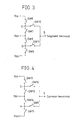
- Figure 3 illustrates the construction of the segment signal circuit that gives to the LCD segment voltage necessary for driving the LCD, by switching the voltage that is output from the boosting circuit.
- Figure 4 illustrates the construction of the common signal circuit that gives to the LCD common voltage necessary for driving the LCD, by switching the voltage that is output from the boosting circuit 1.
- Figure 5 is a diagram for illustrating the operation of the segment signal circuit and the common signal circuit shown in Figs. 3 and 4, respectively. In Fig. 3, the segment signal circuit is constructed by switch SW 6 through switch SW,,.
- the common signal circuit is constructed by switches SW 12 through SW 17 .
- point E To one end (called “point E” hereafter) of the switch SW 12 whose the other end is connected to the V DD terminal of the boosting circuit 1, there are connected one end of the switch SW 13 whose the other end is connected to the V ss1 terminal of the boosting circuit 1, as well as one end of the switch SW 16 whose the other end is connected to the common terminal.
- point F to one end (called “point F” hereafter) of the switch SW, s whose the other end is connected to the V SS2 terminal of the boosting circuit 1, there are connected one end of the switch SW,, whose the other end is connected to the V SS1 terminal of the boosting circuit 1, as well as one end of the switch SW 17 whose the other end is connected to the common terminal.
- the opening and closing at each of the times t, through t7 of the switches SW 6 through SW,, of the segment signal circuit and the switches SW,2 through SW 17 of the common signal circuit are controlled, for example, as shown by the figure, and the voltage that is output from the common terminal is varied with fixed cycle, for example, as +5V ⁇ OV - -5V - OV - + 5 V.
- the segment terminal voltage in response to the common terminal voltage through charge of the voltage between the common and the segment terminals, lighting and nonlighting of the LCD can be accomplished.
- the switches SW 12 , SW, s , and SW 16 of the common signal circuit are in the conducting state while the switches SW 13 , SW,., and SW,7 are in the nonconducting state, so that the common terminal is connected to the V DD terminal via the switches SW,2 and SW 16 and a voltage of + 5V is output on the common terminal.
- the switches SW 6 , SW,, and SW,, of the segment signal circuit are in the conducting state while the switches SW7, SW,, and SW, o are in the nonconducting state, so that the segment terminal is connected to the Vsszterminal via the switches SW 9 and SW,, and a voltage of -5V is output on the segment terminal.
- the voltage between the segment and the common terminals becomes 10V, which is supplied (to the LCD to light up the LCD.
- Hext at time t 2 ,) for example, the switches SW 12 and SW 15 of the common signal circuit are changed from the conducting state to the nonconducting state while the switches SW 13 and SW 14 of the some circuit are changed from the nonconducting state to the conducting state, so that the common terminal is connected to the V SS1 terminal via the switches SW 13 and SW 16 and the common terminal voltage becomes 0V.
- the switches SW 6 and SW 2 of the segment signal circuit are changed from the conducting state to the nonconducting state while the switches SW 7 and SW 8 of the same circuit are changed from the nonconducting state to the conducting state, so that the segment terminal is connected to the V SS1 terminal and the segment terminal voltage becomes 0V. Consequently, the voltage between the segment and the common terminals becomes 0V and the LCD will find itself in the nonlighting condition.
- Analogous situations taking place for time to and thereafter, desired display can be accomplished by realizing the lighting and nonlighting conditions for the LCD according to the following manner. Namely, the LCD is brought to a lighting condition by generating a voltage of 10V between the segment and the common terminals through control of the opening and closing of each of the switches SW 6 through SW 17 of the segment signal circuit and the common signal circuit. Similarly, the LCD may be brought to a nonlighting condition by adjusting to have a voltage of OV impressed between the segment and the common terminals through control of the opening and closing of each of the switches SW 6 through SW 17 .
- the switches SW 6 through SW 17 may become uncontrollable temporarily and behave unstably.
- a control signal such as a power supply shut-off signal or a display erasure instruction signal
- both ends of the boosting capacitor C 2 that is connected in parallel with the switch SW 5 can be short-circuited and the charge that was accumulated on the boosting capacitor C 2 will be discharged. Therefore, between the segment terminal and the common terminal there will not be output a residual voltage, such as the voltage of 10V which is necessary for lighting up the LCD. Therefore, when the power supply is disconnected the content which has been displayed can be erased without, for example, switching of the nonlighting condition of the LCD to the lighting condition with the temporary display of a content which is different from the content that has been displayed on the display until until that time.
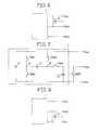
- Figure 6 shows the boosting circuit of the LCD control device for a second embodiment of the invention.
- a special feature of the circuit is to connect a MOS type P-channel transistor in parallel with the boosting capacitor C 2 of the boosting circuit 1 shown in Fig. 1. It discharges the charges that were accumulated on the boosting capacitor C 2 by short-circuiting both ends of the boosting capacitor C2 through conversion of the P-channel transistor from the nonconducting condition to the conducting condition by the use of the same control signal that is used for controlling the switch SW 5 . Therefore, by constructing the circuit as in the above it becomes possible to obtain effects that are similar to those of the first embodiment.
- the component with the same symbol as in Fig. 1 signifies the same item, and its description has been omitted.
- Figure 7 shows the boosting circuit of the LCD control device for a third embodiment of the present invention.
- the boosting circuit 1' shown in Fig. 7 outputs a boosted voltage of positive polarity with respect to the voltage source 3.
- the boosting circuit 1' is constituted by a switch SW3 connected between the V DD1 terminal and one end (called “point B"' hereafter) of the capacitor C, which is connected to one end of the switch SW 4 , a boosting capacitor C o ' which is connected between the other end of the switch SW 4 that is connected to the V DD2 terminal side and the V ss terminal, and a switch SW s ' which is connected in parallel with the boosting capacitor C 2 '.
- the components with the same symbols as in Fig. 1 represent the same items as in Fig. 1, and the explanation on them is omitted.
- a boosting circuit 1' of the above construction first, the switch SW 2 and the switch SW; are in the conducting state, the switch SW, and the switch SW4 are in the nonconducting state, and the capacitor C, is charged to a voltage of +5V with negative charge on the point A side and positive charge on the point B' side. Next, the switch SW, and the switch SW 4 are changed from the nonconducting state to the conducting state, and the switch SW2 and the switch SW 3 ' are changed from the conducting state to the nonconducting state.
- the voltage at point B' is raised from +5V to +10V, which changes the boosting capacitor C o ' to a voltage of + 1 OV and the boosted voltage of + 1 OV is output at the V DD2 terminal.
- the switch SW s ' of the boosting circuit 1' analogous to the switch SW s of the boosting circuit 1, changes from the nonconducting state to the conducting state, and the charges accumulated on the boosting capacitor C 2 ' are discharged by the short-circuiting of both ends of the boosting capacitor C 2 '.
- Figure 8 shows the boosting circuit of the LCD control device relating to a fourth embodiment of the invention.
- a special feature of the device is to connect a MOS type N-channel transistor 11 in parallel with the boosting capacitor C2' of the boosting circuit 1' shown in Fig. 7.
- the N-channel transistor 11 is changed from the nonconducting state to the conducting state by means of the same controlling signal that is used for controlling the switch SWs', to discharge the charges accumulated on the boosting capacitor C o ' by short-circuiting both ends of the boosting capacitor C2'.
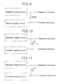
- Figure 9 shows the LCD control device relating to a fifth embodiment of the present invention.
- a special feature of the device consists in connecting a switch SW 18 between the segment terminal of the segment signal circuit shown in Fig. 3 and the common terminal of the common signal circuit shown in Fig. 4.
- the voltage between the segment and the common terminals is made to be less than the voltage for realizing display by liquid crystal, by connecting the segment terminal and the common terminal through change of the switch SW 18 to the conducting state.
- Figure 10 shows the LCD control device relating to a sixth embodiment of the present invention.
- a special feature of the device is that there is connected a MOS type P-channel transistor 13 between the segment terminal and the common terminal as means of short-circuiting the segment terminal and the common terminal at the time of disconnection of the power supply to the LCD device.
- the voltage between the segment and the common terminals is arranged to be reduced to a value which is less than the voltage required for realizing a display by liquid crystal, by changing the P-channel transistor from the nonconducting state to the conducting state.
- Figure 11 shows the LCD Control device relating to a seventh embodiment of the present invention.
- a special feature of the device is that there is connected a MOS type N-channel transistor 15 between the segment terminal and the common terminal as means of short-circuiting the segment and the common terminals at the time of disconnection of the power supply to the LCD device.
- the voltage between the segment and the common terminals is arranged to be reduced to a value which is loss than the voltage required for realizing a display by liquid crystal, by changing the N-channel transistor from the nonconducting state to the conducting state.
- the boosting circuit described in the first and the third embodiments is one that outputs a boosted voltage which is twice as large the voltage of the voltage source, it is of course possible according to the present invention to obtain similar effects by the use of an LCD device which uses a boosting circuit that outputs a boosting voltage that is 2 + N (N ⁇ 1) times that of the power supply.
- the present invention is arranged, when disconnecting the power supply, to discharge quickly the charges that were accumulated on the capacitor for obtaining a voltage that is necessary to drive and display liquid crystal, by carrying out charging and discharging through control of feeding. Therefore, it is possible to provide an LCD control device which is capable, at the time of disconnection of the power supply, of quickly erasing the displayed content, without displaying a content which is different from what has been displayed on the liquid display panel.
Landscapes
- Engineering & Computer Science (AREA)
- Chemical & Material Sciences (AREA)
- Crystallography & Structural Chemistry (AREA)
- Physics & Mathematics (AREA)
- Computer Hardware Design (AREA)
- General Physics & Mathematics (AREA)
- Theoretical Computer Science (AREA)
- Liquid Crystal Display Device Control (AREA)
- Liquid Crystal (AREA)
- Control Of Indicators Other Than Cathode Ray Tubes (AREA)
Applications Claiming Priority (2)
| Application Number | Priority Date | Filing Date | Title |
|---|---|---|---|
| JP60122805A JPS61281293A (ja) | 1985-06-07 | 1985-06-07 | 液晶表示制御装置 |
| JP122805/85 | 1985-06-07 |
Publications (3)
| Publication Number | Publication Date |
|---|---|
| EP0204077A2 true EP0204077A2 (de) | 1986-12-10 |
| EP0204077A3 EP0204077A3 (en) | 1989-05-31 |
| EP0204077B1 EP0204077B1 (de) | 1993-11-10 |
Family
ID=14845070
Family Applications (1)
| Application Number | Title | Priority Date | Filing Date |
|---|---|---|---|
| EP86102855A Expired - Lifetime EP0204077B1 (de) | 1985-06-07 | 1986-03-05 | Flüssigkristallanzeigesteuergerät |
Country Status (4)
| Country | Link |
|---|---|
| US (1) | US4802739A (de) |
| EP (1) | EP0204077B1 (de) |
| JP (1) | JPS61281293A (de) |
| DE (1) | DE3689274T2 (de) |
Cited By (1)
| Publication number | Priority date | Publication date | Assignee | Title |
|---|---|---|---|---|
| EP0847572A1 (de) * | 1996-06-28 | 1998-06-17 | Microchip Technology Inc. | Mikrosteuereinheit mit flüssigkristallanzeigeladungspumpe |
Families Citing this family (29)
| Publication number | Priority date | Publication date | Assignee | Title |
|---|---|---|---|---|
| EP0529701B1 (de) * | 1986-08-18 | 1998-11-11 | Canon Kabushiki Kaisha | Anzeigegerät |
| JPH01134497A (ja) * | 1987-11-20 | 1989-05-26 | Semiconductor Energy Lab Co Ltd | 液晶表示装置の電源回路 |
| JP2546121Y2 (ja) * | 1989-06-23 | 1997-08-27 | 株式会社 東芝 | 液晶表示装置 |
| US5262934A (en) * | 1992-06-23 | 1993-11-16 | Analogic Corporation | Bipolar voltage doubler circuit |
| JPH07120718A (ja) * | 1993-08-31 | 1995-05-12 | Sharp Corp | 液晶表示装置の駆動電圧発生装置 |
| US5552648A (en) * | 1994-02-22 | 1996-09-03 | Delco Electronics Corporation | Method and apparatus for the generation of long time constants using switched capacitors |
| USRE38918E1 (en) | 1994-04-22 | 2005-12-13 | University Of Southern California | System and method for power-efficient charging and discharging of a capacitive load from a single source |
| US5473526A (en) | 1994-04-22 | 1995-12-05 | University Of Southern California | System and method for power-efficient charging and discharging of a capacitive load from a single source |
| JP3577720B2 (ja) | 1995-01-11 | 2004-10-13 | セイコーエプソン株式会社 | 電源回路、液晶表示装置及び電子機器 |
| US5606491A (en) * | 1995-06-05 | 1997-02-25 | Analog Devices, Inc. | Multiplying and inverting charge pump |
| US5768116A (en) * | 1997-01-27 | 1998-06-16 | Honeywell Inc. | Bi-directional DC/DC voltage converter |
| DE69819597T2 (de) * | 1997-05-22 | 2004-09-23 | Sanyo Electric Co., Ltd., Moriguchi | Stromversorgungsschaltung und CCD-Kamera, die diese verwendet |
| US5841648A (en) * | 1997-05-29 | 1998-11-24 | Micro Motion, Inc. | Adjustable voltage converter utilizing a charge pump |
| JP2002506609A (ja) * | 1998-04-24 | 2002-02-26 | コーニンクレッカ、フィリップス、エレクトロニクス、エヌ、ヴィ | 容量性結合型アップダウン変換器 |
| JP2954162B1 (ja) * | 1998-05-20 | 1999-09-27 | 日本電気アイシーマイコンシステム株式会社 | 液晶駆動回路 |
| US6985142B1 (en) * | 1998-09-03 | 2006-01-10 | University Of Southern California | Power-efficient, pulsed driving of capacitive loads to controllable voltage levels |
| JP2000330526A (ja) * | 1999-03-12 | 2000-11-30 | Minolta Co Ltd | 液晶表示装置、携帯電子機器及び駆動方法 |
| US7106318B1 (en) * | 2000-04-28 | 2006-09-12 | Jps Group Holdings, Ltd. | Low power LCD driving scheme employing two or more power supplies |
| US20050077950A1 (en) * | 2003-10-14 | 2005-04-14 | Robinson Curtis B. | Negative charge pump |
| JP4001856B2 (ja) * | 2003-10-30 | 2007-10-31 | ローム株式会社 | 発光素子駆動装置、発光素子駆動装置を有する表示モジュール及び、表示モジュールを備えた電子機器 |
| JP2005151777A (ja) * | 2003-11-19 | 2005-06-09 | Sanyo Electric Co Ltd | チャージポンプ回路およびアンプ |
| JP4634154B2 (ja) * | 2004-01-06 | 2011-02-16 | パナソニック株式会社 | 昇圧回路 |
| TWI250719B (en) * | 2004-04-02 | 2006-03-01 | Au Optronics Corp | DC-DC converter |
| JP4511288B2 (ja) * | 2004-09-01 | 2010-07-28 | 三洋電機株式会社 | チャージポンプ回路 |
| JP4699851B2 (ja) * | 2005-09-30 | 2011-06-15 | ルネサスエレクトロニクス株式会社 | 昇圧回路 |
| WO2011045671A2 (en) * | 2009-10-14 | 2011-04-21 | Energy Micro AS | Liquid crystal display driver |
| JP5915498B2 (ja) * | 2012-10-26 | 2016-05-11 | 株式会社島津製作所 | 重水素ランプ用電源回路 |
| CN105446402B (zh) * | 2014-08-04 | 2017-03-15 | 北京大学深圳研究生院 | 可控电压源、移位寄存器及其单元和一种显示器 |
| CN111857264B (zh) * | 2020-07-03 | 2022-04-12 | Oppo广东移动通信有限公司 | 电源电路及电子设备 |
Citations (1)
| Publication number | Priority date | Publication date | Assignee | Title |
|---|---|---|---|---|
| US4186436A (en) * | 1977-01-27 | 1980-01-29 | Canon Kabushiki Kaisha | Booster circuit |
Family Cites Families (10)
| Publication number | Priority date | Publication date | Assignee | Title |
|---|---|---|---|---|
| CH509638A (fr) * | 1967-12-21 | 1971-06-30 | Philips Nv | Dispositif de prolongation automatique du temps de feu vert d'une installation de signalisation |
| NL7116944A (de) * | 1971-12-09 | 1973-06-13 | ||
| JPS5731148B2 (de) * | 1973-05-15 | 1982-07-02 | ||
| JPS51132940A (en) * | 1975-05-14 | 1976-11-18 | Sharp Corp | Electric source apparatus |
| JPS5211898A (en) * | 1975-07-18 | 1977-01-29 | Seiko Epson Corp | Liquid crystal dispiay equipment |
| JPS5229925A (en) * | 1975-09-01 | 1977-03-07 | Seiko Instr & Electronics Ltd | Voltage step-up circuit |
| JPS5838770B2 (ja) * | 1975-10-15 | 1983-08-25 | セイコーエプソン株式会社 | エキシヨウヒヨウジソウチ |
| JPS6051714B2 (ja) * | 1977-03-29 | 1985-11-15 | セイコーエプソン株式会社 | 液晶表示装置駆動回路 |
| JPS6117127A (ja) * | 1984-07-04 | 1986-01-25 | Hitachi Ltd | 光スイツチ素子の駆動方法 |
| US4636930A (en) * | 1985-10-01 | 1987-01-13 | Maxim Integrated Products, Inc. | Integrated dual charge pump power supply and RS-232 transmitter/receiver |
-
1985
- 1985-06-07 JP JP60122805A patent/JPS61281293A/ja active Pending
-
1986
- 1986-02-27 US US06/833,233 patent/US4802739A/en not_active Expired - Lifetime
- 1986-03-05 EP EP86102855A patent/EP0204077B1/de not_active Expired - Lifetime
- 1986-03-05 DE DE86102855T patent/DE3689274T2/de not_active Expired - Fee Related
Patent Citations (1)
| Publication number | Priority date | Publication date | Assignee | Title |
|---|---|---|---|---|
| US4186436A (en) * | 1977-01-27 | 1980-01-29 | Canon Kabushiki Kaisha | Booster circuit |
Cited By (3)
| Publication number | Priority date | Publication date | Assignee | Title |
|---|---|---|---|---|
| EP0847572A1 (de) * | 1996-06-28 | 1998-06-17 | Microchip Technology Inc. | Mikrosteuereinheit mit flüssigkristallanzeigeladungspumpe |
| US5861861A (en) * | 1996-06-28 | 1999-01-19 | Microchip Technology Incorporated | Microcontroller chip with integrated LCD control module and switched capacitor driver circuit |
| EP0847572A4 (de) * | 1996-06-28 | 1999-10-20 | Microchip Tech Inc | Mikrosteuereinheit mit flüssigkristallanzeigeladungspumpe |
Also Published As
| Publication number | Publication date |
|---|---|
| EP0204077A3 (en) | 1989-05-31 |
| US4802739A (en) | 1989-02-07 |
| DE3689274D1 (de) | 1993-12-16 |
| EP0204077B1 (de) | 1993-11-10 |
| DE3689274T2 (de) | 1994-04-28 |
| JPS61281293A (ja) | 1986-12-11 |
Similar Documents
| Publication | Publication Date | Title |
|---|---|---|
| EP0204077A2 (de) | Flüssigkristallanzeigesteuergerät | |
| KR100438205B1 (ko) | 구동회로, 충전/방전회로 및 액정표시장치 | |
| US8125432B2 (en) | Common voltage generation circuit employing a charge-pump operation to generate low-potential-side voltage | |
| US20070262976A1 (en) | Level Shifter Circuit, Driving Circuit, and Display Device | |
| JP3150127B2 (ja) | 昇圧回路 | |
| US7733160B2 (en) | Power supply circuit, display driver, electro-optical device, and electronic instrument | |
| US20080068316A1 (en) | Driver circuit, electro-optical device, and electronic instrument | |
| JP4421208B2 (ja) | レベルシフタ回路およびそれを備えた表示装置 | |
| EP0434841B1 (de) | Leistungsquellenschaltung | |
| US8754838B2 (en) | Discharge circuit and display device with the same | |
| WO2004066246A1 (ja) | 表示装置 | |
| US20080303586A1 (en) | Negative voltage generating circuit | |
| US4958151A (en) | Display control circuit | |
| US20040095306A1 (en) | Driving circuit for driving capacitive element with reduced power loss in output stage | |
| US7230471B2 (en) | Charge pump circuit of LCD driver including driver having variable current driving capability | |
| US6084580A (en) | Voltage generating circuit and liquid crystal display device incorporating the voltage generating circuit | |
| US7088356B2 (en) | Power source circuit | |
| JPH07235844A (ja) | アナログドライバicの出力バッファ回路 | |
| US20080122826A1 (en) | Driving circuit for adjusting common voltage and liquid crystal display using same | |
| JP3799869B2 (ja) | 電源回路を搭載した半導体装置並びにそれを用いた液晶装置及び電子機器 | |
| JPH09318927A (ja) | 液晶表示装置 | |
| US7545170B2 (en) | Source driver and level shifting method thereof | |
| JP4498073B2 (ja) | チャージポンプ回路 | |
| CN114495856B (zh) | 像素电路及其驱动方法、显示装置 | |
| KR100543038B1 (ko) | 박막 트랜지스터 액정 표시 장치의 구동 신호 제어 회로 |
Legal Events
| Date | Code | Title | Description |
|---|---|---|---|
| PUAI | Public reference made under article 153(3) epc to a published international application that has entered the european phase |
Free format text: ORIGINAL CODE: 0009012 |
|
| 17P | Request for examination filed |
Effective date: 19860305 |
|
| AK | Designated contracting states |
Kind code of ref document: A2 Designated state(s): DE FR GB |
|
| PUAL | Search report despatched |
Free format text: ORIGINAL CODE: 0009013 |
|
| AK | Designated contracting states |
Kind code of ref document: A3 Designated state(s): DE FR GB |
|
| 17Q | First examination report despatched |
Effective date: 19920224 |
|
| GRAA | (expected) grant |
Free format text: ORIGINAL CODE: 0009210 |
|
| AK | Designated contracting states |
Kind code of ref document: B1 Designated state(s): DE FR GB |
|
| REF | Corresponds to: |
Ref document number: 3689274 Country of ref document: DE Date of ref document: 19931216 |
|
| ET | Fr: translation filed | ||
| PLBE | No opposition filed within time limit |
Free format text: ORIGINAL CODE: 0009261 |
|
| STAA | Information on the status of an ep patent application or granted ep patent |
Free format text: STATUS: NO OPPOSITION FILED WITHIN TIME LIMIT |
|
| 26N | No opposition filed | ||
| PGFP | Annual fee paid to national office [announced via postgrant information from national office to epo] |
Ref country code: FR Payment date: 19980310 Year of fee payment: 13 |
|
| PGFP | Annual fee paid to national office [announced via postgrant information from national office to epo] |
Ref country code: DE Payment date: 19980313 Year of fee payment: 13 |
|
| REG | Reference to a national code |
Ref country code: GB Ref legal event code: 746 Effective date: 19981008 |
|
| PG25 | Lapsed in a contracting state [announced via postgrant information from national office to epo] |
Ref country code: FR Free format text: LAPSE BECAUSE OF NON-PAYMENT OF DUE FEES Effective date: 19991130 |
|
| REG | Reference to a national code |
Ref country code: FR Ref legal event code: ST |
|
| PG25 | Lapsed in a contracting state [announced via postgrant information from national office to epo] |
Ref country code: DE Free format text: LAPSE BECAUSE OF NON-PAYMENT OF DUE FEES Effective date: 20000101 |
|
| REG | Reference to a national code |
Ref country code: GB Ref legal event code: IF02 |
|
| PGFP | Annual fee paid to national office [announced via postgrant information from national office to epo] |
Ref country code: GB Payment date: 20050302 Year of fee payment: 20 |
|
| PG25 | Lapsed in a contracting state [announced via postgrant information from national office to epo] |
Ref country code: GB Free format text: LAPSE BECAUSE OF EXPIRATION OF PROTECTION Effective date: 20060304 |
|
| REG | Reference to a national code |
Ref country code: GB Ref legal event code: PE20 |