EP0201282A2 - Dispositif d'ajustement de position avec un élément piézoélectrique comme mécanisme d'arrêt - Google Patents
Dispositif d'ajustement de position avec un élément piézoélectrique comme mécanisme d'arrêt Download PDFInfo
- Publication number
- EP0201282A2 EP0201282A2 EP86303311A EP86303311A EP0201282A2 EP 0201282 A2 EP0201282 A2 EP 0201282A2 EP 86303311 A EP86303311 A EP 86303311A EP 86303311 A EP86303311 A EP 86303311A EP 0201282 A2 EP0201282 A2 EP 0201282A2
- Authority
- EP
- European Patent Office
- Prior art keywords
- voltage
- piezoelectric element
- holder
- support means
- wafer
- Prior art date
- Legal status (The legal status is an assumption and is not a legal conclusion. Google has not performed a legal analysis and makes no representation as to the accuracy of the status listed.)
- Granted
Links
Images


Classifications
-
- G—PHYSICS
- G03—PHOTOGRAPHY; CINEMATOGRAPHY; ANALOGOUS TECHNIQUES USING WAVES OTHER THAN OPTICAL WAVES; ELECTROGRAPHY; HOLOGRAPHY
- G03F—PHOTOMECHANICAL PRODUCTION OF TEXTURED OR PATTERNED SURFACES, e.g. FOR PRINTING, FOR PROCESSING OF SEMICONDUCTOR DEVICES; MATERIALS THEREFOR; ORIGINALS THEREFOR; APPARATUS SPECIALLY ADAPTED THEREFOR
- G03F7/00—Photomechanical, e.g. photolithographic, production of textured or patterned surfaces, e.g. printing surfaces; Materials therefor, e.g. comprising photoresists; Apparatus specially adapted therefor
- G03F7/70—Microphotolithographic exposure; Apparatus therefor
- G03F7/70691—Handling of masks or workpieces
- G03F7/707—Chucks, e.g. chucking or un-chucking operations or structural details
-
- B—PERFORMING OPERATIONS; TRANSPORTING
- B23—MACHINE TOOLS; METAL-WORKING NOT OTHERWISE PROVIDED FOR
- B23Q—DETAILS, COMPONENTS, OR ACCESSORIES FOR MACHINE TOOLS, e.g. ARRANGEMENTS FOR COPYING OR CONTROLLING; MACHINE TOOLS IN GENERAL CHARACTERISED BY THE CONSTRUCTION OF PARTICULAR DETAILS OR COMPONENTS; COMBINATIONS OR ASSOCIATIONS OF METAL-WORKING MACHINES, NOT DIRECTED TO A PARTICULAR RESULT
- B23Q1/00—Members which are comprised in the general build-up of a form of machine, particularly relatively large fixed members
- B23Q1/25—Movable or adjustable work or tool supports
- B23Q1/26—Movable or adjustable work or tool supports characterised by constructional features relating to the co-operation of relatively movable members; Means for preventing relative movement of such members
- B23Q1/28—Means for securing sliding members in any desired position
-
- B—PERFORMING OPERATIONS; TRANSPORTING
- B23—MACHINE TOOLS; METAL-WORKING NOT OTHERWISE PROVIDED FOR
- B23Q—DETAILS, COMPONENTS, OR ACCESSORIES FOR MACHINE TOOLS, e.g. ARRANGEMENTS FOR COPYING OR CONTROLLING; MACHINE TOOLS IN GENERAL CHARACTERISED BY THE CONSTRUCTION OF PARTICULAR DETAILS OR COMPONENTS; COMBINATIONS OR ASSOCIATIONS OF METAL-WORKING MACHINES, NOT DIRECTED TO A PARTICULAR RESULT
- B23Q1/00—Members which are comprised in the general build-up of a form of machine, particularly relatively large fixed members
- B23Q1/25—Movable or adjustable work or tool supports
- B23Q1/26—Movable or adjustable work or tool supports characterised by constructional features relating to the co-operation of relatively movable members; Means for preventing relative movement of such members
- B23Q1/34—Relative movement obtained by use of deformable elements, e.g. piezoelectric, magnetostrictive, elastic or thermally-dilatable elements
Definitions
- the present invention relates to a position adjustment device and, in particular, to a position adjustment device using a piezoelectric displacement device which deforms in response to an applied voltage to precisely adjust an object to a reference position.
- Position alignment or adjustment devices have been used in various kinds of technical fields in order to precisely adjust the position of an object, such as a semiconductor wafer in an electron beam fine pattern exposure system, an optical coupling element in an optical communication system, etc.
- One such device is known which is used to adjust the position of a semiconductor wafer set in the pattern exposure apparatus in such a manner that the surface of the wafer coincides with the known reference surface of a sample table unit.
- This position alignment of the semiconductor wafer should be carried out with high accuracy. Otherwise, an image of the mask pattern will not be just-focussed onto the wafer, and it will be impossible to transfer the electron beam pattern onto the wafer precisely.
- a semiconductor wafer is position-adjusted manually by an operator and then fixed to the last determined position by using mechanical fixation means. More specifically, the semiconductor wafer, onto which the mask pattern is to be transferred, is placed within a wafer supporting member, known as "wafer cassette holder", and then put on a known table plate defining a reference surface.
- the wafer holder is arranged such that it can move up and down on the table to vary the height of the wafer surface with respect to the reference surface.
- the height of the wafer holder is adjusted to cause the wafer surface, onto which a beam pattern will be transferred, to be in precisely coincidence with the reference surface.
- the wafer holder is then locked mechanically, so that the wafer is held at the same level as the reference surface.
- a plurality of rods are movably provided in the cylindrical holes cut in the wafer cassette holder. They can vertically move in the holes and serve as support legs for the wafer holder set on the table plate. When the rods project downward from the holes to push the table surface, the wafer holder may be lifted up on the table. The wafer holder may fall down when these rods are moved back and pulled into the holes. Therefore, by changing the distance the movable rods move from the holes, which corresponds to the leg length of the wafer, the wafer surface can be precisely aligned with the reference surface of the sample table.
- each rod should be rigidly clamped in the corresponding hole to hold the wafer cassette holder at the finally adjusted height.
- Screws are usually provided in the wafer holder for clamping the rods inside the holes.
- it is very difficult to keep holding the wafer accurately at the last adjusted height while the screws are being rotated to compress and lock the leg rods. This is because the mechanical vibration caused by rotating the screws makes the surface of the wafer set in the cassette holder move from the just- adjusted position as it is applied to the wafer cassette holder.
- the rods are being compressed by screws, the precise position adjustment cannot be achieved if the wafer holder is inclined or misaligned again with respect to the reference surface due to the mechanical vibration.
- An adjustment of the wafer position on the order of microns or, more precisely, of sub- microns, is far from possible.
- the present invention is addressed to a specific device which includes a mechanical support member for supporting an object and for adjusting the position of the object.
- a piezoelectric element is used as a clamping mechanism for locking or unlocking the support member. It deforms or distorts in accordance with an electric field generated in it in response to the application of a drive voltage.
- the piezoelectric element is specially designed to lock or unlock the support member.
- the element contracts to unlock the support member and allows the member to move for adjusting the position of the object.
- the element expands to its original size, clamping the support member.
- the support member is thus stably fixed or clamped in its last adjusted position, where it supports the object in a desired position. Since the support member is effectively locked or clamped by the expanded piezoelectric element under no bias condition, there is no need to continuously supply with the element any kind of drive voltage.
- the piezoelectric element can be disconnected from a voltage source circuit after the position adjustment is completed for the object.
- a wafer alignment device designated generally by the numeral 10.
- This wafer alignment device 10 is used for a known electron beam pattern exposure system (not shown in Fig. 1), wherein a mask pattern is transferred onto a semiconductor wafer by using electron beam.
- a typical arrangement of such the electron beam pattern exposure system is known among skilled persons and is described in United State Patent No. 4,558,225 to GOTOU et al., for example.
- the use of the wafer alignment device 10 enables the position adjustment of the semiconductor wafer to be more precise and accurate, without degrading the positioning speed.
- Semiconductor wafer 12 onto which a mask pattern is to be transferred is comprised of a signal-crystalline silicon plate having a thin-disk shape.
- This wafer 12 is electrostatically attached by known means to a substrate 14, which is loaded in a square box-shaped cassette holder 16 made of metal. Wafer 12 is thus fixedly mounted on the lower surface of wafer holder 16.
- wafer holder 16 is put on a known surface plate 18 having its upper surface which defines a reference surface 20. Holder 16 is placed on the reference surface plate 18 such that a surface of wafer 12, onto which a beam pattern is to be transferred, is full area-to-area contact with the reference surface 20 as shown in Fig. 1.
- Holder 16 has a plurality of vertically-extended cylindrical openings 22.
- four cylindrical openings are formed in wafer holder 16 at four corners thereof, although only two openings 22A and 22B are illustrated in cross-sectional view of Fig. 1.
- suffixes A and B may be dropped, if there is no need to particularly distinguish between them.
- Each rod 24 is so arranged as to be freely movable in the corresponding cylindrical opening 22 along a direction perpendicular to the reference surface 20.
- holder 16 When being mounted on surface plate 18, holder 16 may be also supported by four rods 24 on reference surface 20, if these rods are fixed by clamping mechanism in cylindrical openings 22.
- Each metal rod 24 has distal ends of half-ball shape as shown in Fig. 1.
- Rods 24 serve as support legs for the main body of wafer holder 16.
- Rods 24 can be in point-contact with reference surface 20. It is thus possible to facilitate well-stabilized positioning of holder 16 on reference surface 20 of plate 18.
- the same number of, four, piezoelectric elements 26 are necessary to clamp leg rods 24 independently.
- Piezoelectric elements 26 are housed in the corresponding room spaces, which are formed in holder 16 so as to be coupled with the middle portions of cylindrical openings 22, respectively.
- the room spaces are extended horizontally to be coupled with the vertical cylindrical openings 22 at their ends.
- Each cylindrical opening 22 and the corresponding room space forms inside holder 16 an opening of T-shaped cross section as shown in Fig. 1.
- Each piezoelectric elements 26 is mechanically de - formed or distorted along its longitudinal direction in accordance with a voltage applied thereto.
- piezoelectric elements 26 When piezoelectric elements 26 is longitudinally expanded toward the cylindrical opening 22 and its free end presses the round side wall of the corresponding leg rod 24, the movement of rod 24 in opening 22 is extremely restricted due to the mechanical contact force (i.e., clamping pressure) generated between the leg rod and the piezoelectric element.
- the piezoelectric element 26 is further expanded in response to increase in the applied voltage, the reciprocal movement of leg rod 24 in opening 22 is no longer permitted, so that the rod is fixed to the last adjusted position in the opening. In this sense, piezoelectric elements 26 serve as a locking mechanism for slidable rods 24 in openings 22 of wafer holder 16.
- leg rods 24 are unloosed so that the lower surface of wafer 14 and the rounded low ends of pins 22 are indirect contact with the reference surface 20. Under this condition, the wafer surface onto which an electron beam pattern is to be transferred precisely coincides with the reference surface 20. If all the rod pins 22 are locked by the corresponding piezoelectric elements 26, the low ends of rods 24 and the patterning surface of wafer 12 are kept identical with each other, even after wafer holder 16 is removed from surface plate 18.
- Wafer holder 16 is provided with connect pins 28A, 28B,...which are electrically connected to piezoelectric elements 26A, 26B,..., respectively. These connect pins 28 are expandable, by the elastic force of springs (not shown) provided therein, vertically with respect to the lower surface of wafer holder 16.
- contact pins 28A, 28B,... project downward to be in contact with metal pads 30A, 30B,..., which are formed on the reference surface 20 of surface plate 18.
- piezoelectric elements 26 are electrically connected with the corresponding contact pads 30, while wafer holder 16 is placed on plate 18.
- a voltage generating circuitry 32 is connected to contact metal pads 30 formed on surface plate 18. Voltage generator 32 is thus connected with piezoelectric elements 26 housed in wafer holder 16, which is placed on surface plate 18. Under this condition, voltage generator 32 supplies a variable DC voltage which causes electric fields of different intensities to be formed in piezoelectric elements 26, respectively.
- Voltage generator 32 includes independent DC voltage source units 34A, 34B,...which feed the corresponding piezoelectric elements 26A, 26B,...embedded in wafer holder 16.
- DC voltage source units 34A, 34B which feed the corresponding piezoelectric elements 26A, 26B,...embedded in wafer holder 16.
- Voltage source unit 32A is electrically connected with piezoelectric element 28A, and unit 32B with element 28B.
- Voltage source unit 36A includes a switch 38A which has a common terminal connected to piezoelectric element 26A through lead wire 34A.
- Switch 36A has three voltage input terminals. The first voltage input terminal is connected to a battery generating a positive polarity of DC voltage +Ea, the second terminal grounded, and the third terminal a battery generating a negative polarity of DC voltage -Eb.
- Voltage source unit 36B is connected with piezoelectric element 26B through a lead wire 34B and includes a switch 38B which has the same configuration as that in voltage source unit 36A, so that the detailed description thereof will be omitted by using the same reference numerals with the corresponding suffix B.
- Fig. 2 shows wafer holder 16 which is set in a sample support unit 40 provided in an electron beam pattern exposure apparatus, after the position adjustment of rods 24 is completed.
- Support unit 40 has a square-shaped frame 42 for housing wafer holder 16 therein.
- Frame 42 defines a vertical guide wall 44 with which the side surface of wafer holder 16 is in contact as shown in Fig. 2.
- a horizontal table plate 46 is formed on the upper end of frame 42 to cover the upper opening thereof.
- Table plate 46 has an opening 48 through which an electron beam pattern 50 is radiated onto the pattern transfer surface, i.e., the top surface of semiconductor wafer 12.
- Table plate 46 defines at its lower surface a reference surface 52 for just-focussing the beam pattern.
- Table plate 46 defines at its lower surface a reference surface 52 for just-focussing the beam pattern.
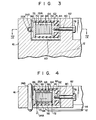
- FIG. 3 is a plan view partially showing wafer holder 16, so that leg rod 24A, which is used to adjust the height of holder 16 with respect to the reference surface, is illustrated as a circle.
- a metal case unit 62 which is formed almost like a rectangular box whose one end opposing leg rod 24A is opened.
- An inner housing 64 is tightly placed in metal case unit 42.
- Inner housing 64 is made hollow so that it can hold therein piezoelectric element 26A.
- Inner housing 64 is made of insulative material so as to electrically separate piezoelectric element 26A from metal case unit 62.
- Piezoelectric element 26A is comprised of a multi-layered piezoelectric ceramic device having a plurality of thin piezoelectric disc plates 66 disposed one above another as shown in Fig. 3, so that piezoelectric element 26A looks like a solid cylinder as a whole. These piezoelectric disc plates 66 are polarized in the direction of plate thickness, and are stacked in such a manner that the polarization direction of two adjacent piezoelectric plates are reversed in relation to each other. Wiring electrode layers 68 are sandwiched between piezoelectric disc plates 66. Insulative plates 70 and 72 are attached to the both ends of cylindrical piezoelectric element 26A, which is sandwiched between metal fixtures 74 and 76 in metal case 62 housed in room space 60 of wafer holder 16.
- One metal fixture 74 to which piezoelectric element 26A is adhered at its bottom, is placed at the bottom portion of insulative inner housing 64.
- Metal fixture 74 is locked by a screw 78, which penetrates through a hole 80 formed in a frame wall 82 of wafer holder 16 to be mechanically coupled with a negative screw 84 formed in metal fixture 74.
- the other metal fixture 76 is adhered to electrode layer 70 at the top portion of piezoelectric element 26A.
- Metal fixture 76 is positioned to cover the open end of insulative inner housing 64 as if it were a lid for a vessel. Lid-shaped metal fixture 76 is formed such that its peripheral edge is just fitted with the inner wall of housing 64 and that it is movable inside this housing 64.
- lid-shaped metal fixture 76 When piezoelectric element 26A is physically deformed along its longitudinal direction in response to an applied voltage, lid-shaped metal fixture 76 may reciprocate in accordance with the linear expansion or shrinkage of piezoelectric element 26A.
- a cylindrical projection 86 is formed on metal fixture 76 at the center thereof in such a manner that this projection 86 is in direct contact with the side wall of leg rod 24A movably put in vertical opening 22A of wafer holder 16. Therefore, when piezoelectric element 26A is expanded, rod 24A will be fixed due to direct compression pressure of cylindrical projection 86 of lid-shaped metal fixture 76.
- Wiring electrode layers 68 are connected in common to a first lead wire 90 at every other electrode layers as illustrated in Fig. 4. The remaining layers of wiring electrode layers 68 are connected in common with a second lead wire 92.
- First lead wire 90 is electrically connected to lid-shaped metal fixture 76, while second lead wire 92 is connected with voltage source line 34A to which a variable DC voltage is supplied by voltage generator 32 shown in Fig. 1.
- Lid-shaped metal fixture 76 is electrically conducted with metal holder 16 by the way of position determining leg rod 24A whose round side wall is in contact with the inner surface of opening 22A of wafer holder 16. Therefore, when a DC voltage is applied by voltage generator 32 (Fig. 1) between line 34A and holder 16, the DC voltage is also applied between first and second lead wires 90 and 92 of piezoelectric element 26A embedded in wafer holder 16. In response to the voltage application, piezoelectric element 26A extends or contracts (expands or shrink) in its longitudinal direction shown by an allow 94 in Fig. 4, thus generating displacement.
- Fig. 5 shows a hysteresis characteristic of the piezoelectric element used as the lock mechanism.
- the changes in the amount of displacement Dm of piezoelectric element 26 when voltage E is applied thereto are known as "butterfly characteristics" to one skilled in the art, since the shape of the characteristic curve resembles a butterfly with its wings open.
- the voltage point of a supply voltage from DC voltage source +Ea of voltage generator 32 shown in Fig. 1 is plotted as "+Ea”.
- the supply voltage from DC voltage source -Eb is plotted as "-Eb”.
- amount of displacement Dm of element 26 varies as indicated by broken lines "c", “d”, “e”, and “f".
- Inflection point B between curves "c” and “d” corresponds to the voltage supplied from DC voltage source -Eb of voltage generator 32.
- negative voltage -Eb used herein defines an electric field (coercive electric field) in which the polarization direction in element 26 is inverted.
- amount of displacement Dm occurring in element 26 has butterfly characteristics. The hysteresis characteristics themselves are generally known.
- leg rods 24 are unlocked and the pattern transfer surface of semiconductor wafer 12 contacts reference surface 20 of plate 12.
- the rounded lower ends of rods 24 coincide precisely with the pattern transfer surface of wafer 12.
- a voltage varying between two voltage levels +Ea and -Eb is applied to element 26, and the hysteresis curve of displacement Dm occurring in element 26 is that indicated by solid curve 96 in Fig. 5.
- amount of displacement Dm of element 26 changes along different curves in accordance with the increase or decrease in the electric field (see line 96 in Fig. 5).
- Piezoelectric element 26 of wafer holder 16 placed on surface plate 18 is connected to voltage generator 32 by lead wire 34 through a detachable electrical connection constituted by connect pin 28 and metal pad pattern 30, as previously described.
- switches 38 of generator 32 are switched (to the first state of Fig. 1) to connect DC batteries +Ea to elements 26A, 26B..., positive voltage +Ea is supplied to each element 26.
- switches 38 are switched to the second state, elements 26A, 26B,...are grounded.
- switches 38 are switched to the third state, elements 26A, 26B,...are connected to DC batteries -Eb for generating a negative voltage for defining a polarization inversion electric field (coercive electric field) of element 26.
- switches 38 of generator 32 are switched to the second state to cause elements 26A, 26B,...to be grounded.
- Amount of displacement Dm of element 26 to which no voltage is applied changes along curve "g", connecting points B and E in Fig. 5, and reaches point E.
- a displacement corresponding to point E remains in element 26 despite the fact that the applied voltage is 0.
- Switches 38 are then switched to the first state to supply positive voltage +Ea to element 26.
- Element 26 is then elongated longitudinally, and its amount of displacement Dm varies along curve "h", connecting points E and A, and reaches point A.
- element 26 is set at ground voltage so that amount of displacement Dm of element 26 varies along curve "b", to return to the initial state, i.e., a 0 displacement state.
- the displacement of element 26 under the non-bias state is theoretically 0.
- element 26 is considered to be elongated when compared with the case wherein negative voltage -Eb defining the polarization inversion electric field (coercive electric field) is applied.
- a gap (called "initial gap") between the free end of element 26 and the side wall of the corresponding leg rod is designed such that element 26 can lock rods 24.
- the initial gap between the distal end of projection 86 of lid-like fixture 76, bonded to element 26 and the side wall of rod 24 shown in Fig. 4, is designed to be smaller than the displacement indicated by point E in Fig. 5.
- the practical initial gap between element 26 and the rod was selected to be, e.g., as small as about half to one third the displacement indicated by point E in Fig. 5 in order to completely clamp the rod with element 26 in the non-bias state.
- element 26 has a Young's modulus as large as possible and a high Curie temperature, and that amount of displacement Dm is as large as possible (e.g., element 26 is an integrally molded multi-layered piezoelectric ceramic element).
- leg rods 24 were locked after completion of position alignment of wafer 12 on surface plate 18, they were locked with a sufficiently large clamping pressure, thus allowing no loosening. Thereafter, when wafer holder 16 was picked up from surface plate 18 and housed in an electronic beam pattern exposure system, wafer 12 was actually positioned with high precision, and no positioning error with respect to a reference surface of the system occurred.
- the initial gap between leg rod 24 and projection 86 of metal fixture 76 was set to 10 ⁇ m, and the displacement amount of 5 ⁇ m was used to generate a clamping pressure to lock leg rod 24 to wafer holder 16. With this structure, it was confirmed that holder 16 was not moved downward against a load weight of up to 2 kg, and a sufficient locking force was obtained.
- rods 24 are fixed in openings 22 using a piezoelectric element having amount of displacement Dm which varies in accordance with a bias voltage.
- the clamping pressure for fixing rods 24 is constant so that they can be locked by a uniform force.
- Rods 24 are locked by element 26 in a non-bias state, i.e., in a state where no voltage is externally supplied. Therefore, rods 24 can be fixed effectively without being influenced by ambient conditions (e.g., a change in ambient temperature).
- FIG. 6 shows a position adjustment device for an optical coupling unit used in a optical communication system.
- a base table 100 is provided with a vertical opening 102 in which a holder 104 is inserted movably.
- Holder 104 rigidly supports at its top portion an optical signal transmission cable 106, such as an optical fiber. More specifically, holder 104 consists of a head portion 104a and a straight leg portion 104b which is inserted into opening 102.
- a V-shaped groove 108 is formed in the top surface of holder head portion 104a.
- Optical fiber cable 106 is fixed in the V-shaped groove 108 by a known adhesion means 110, such as a solder, adhesive material, etc.
- Cable 106 is thus placed to extend in parallel with the top surface of base table 100 and optically connected at one distal end thereof with a known light emitting element (not shown), which generates an optical signal representing a digital signal to be transmitted in a known manner.
- Optical fiber cable 106 radiates an optical signal, which is transmitted therethrough from light emitting element, at the other distal end thereof.
- This cable end designated by numeral "112" in Fig. 6, is immovable with respect to the movable cable holder 104.
- the height of the cable end 112 may be changed with respect to base table 100, since cable holder 104 can be movable upward or downward in vertical opening 102 of base table 100.
- base table 100 On base table 100 is also provided a support block l14 on which a photodetector 116 is fixed as a light signal receiving element.
- Photodetector 116 may be a known photodiode, for example.
- Support block 114 is fixedly mounted on table 100, so that photodetector 116 is inmovably positioned over base table 100. It should be required that optical fiber cable 106 and photodetector 116 are optically connected with each other in such a manner that cable 106 is linearly aligned with photodetector 116 to form an optical signal transmission path.
- a piezoelectric element 120 is embedded in base table 100 as a clamping mechanism for vertically movable cable holder 104. Piezoelectric element 120 is placed within a room space 122 together with an insulative inner housing 124 and metal fixture plates 126 and 128. Room space 122 is so formed in table 100 as to be coupled with the middle portion of vertical opening 102. Room space 122 is extended horizontally and coupled with vertical opening 103 at its end. Vertical opening 102 in which cable holder 104 is placed and room space 122 forms inside table 100 an opening of T-shaped cross section as shown in Fig. 6.
- Piezoelectric element 120 is placed in insulative housing 122 and two metal plates 126 and 128 are attached to the top and bottom portions of piezoelectric element 120, respectively, as clearly shown in Fig. 6.
- Piezoelectric element 120 may be a multi-layered piezoelectric ceramic device, which is same as that used in the first embodiment shown in Fig. 1. Piezoelectric element 120 is deformed or distorted along its longitudinal direction 130 in accordance with a voltage applied thereto. When piezoelectric element 120 is expanded longitudinally toward the opening 102 and its free end presses the side wall of cable holder 104, the movement of holder 104 inside opening 102 is extremely restricted due to the clamping pressure of piezoelectric element 120.
- piezoelectric element 120 When piezoelectric element 120 is further expanded, the reciprocal movement of cable holder 104 is no longer permitted, so that holder 104 is fixed to the last adjusted position in opening 102 of base table 100. Therefore, piezoelectric element 120 can serve as a locking mechanism for cable holder 104.
- cable holder 104 When the position adjustment is carried out for optical fiber cable 106, cable holder 104 is unlocked so that the height of holder 104 with respect to the top table surface can be manually adjusted by an operator by moving cable holder 104 along the vertical direction, designated by an allow 132. After the position adjustment is completed, cable holder 104 is locked by piezoelectric element 126, so that the cable end 112 can be positioned to be aligned with photodetector 116 fixed on block 114.
- a voltage generating circuitry 134 is connected to piezoelectric element for supplying a variable DC voltage which causes an electric filed of different intensities to be formed in piezoelectric element 120.
- Voltage generator 30 includes a DC voltage source unit 136 including two DC voltage sources 138 and 140, and a switch 138 which switches to selectively supply piezoelectric element 120 with DC voltages +Ea or -Eb generated by the voltage sources, or ground potential. It should be noted that voltage generator 134 is connected to piezoelectric element 120 through a lead wire 144. Voltage generator 134 is disconnectable from piezoelectric element 120 embedded in table 100, since lead wire 144 is connected with piezoelectric element 120 through a known type of electrical connector 146.
- each magnetic video head is mounted on a head holder which is movably provided on a rotatable drum.
- Piezoelectric elements are embedded in the drum to control the movement of head holders in such a manner as to carry out the accurate position-adjustment of each magnetic head, independently.
- a negative polarity of DC voltage is applied by a voltage source circuit to the piezoelectric elements to thereby cause the head holders to be unloosed.
- the position adjustment of each magnetic head can be performed by an operator. After the completion of the position adjustment, the piezoelectric elements are connected to the ground, so that they clamp the corresponding head holders which are thus locked to the last adjusted positions, respectively. After all the head holders are locked, the voltage source circuit is disconnected from the head drum. Even under this condition, the hard holders are kept fixed to the position lastly determined by the operator, since the full mechanical clamping of the head holder by the piezoelectric element is carried out under no bias condition.
Landscapes
- Engineering & Computer Science (AREA)
- Mechanical Engineering (AREA)
- Physics & Mathematics (AREA)
- General Physics & Mathematics (AREA)
- Electron Beam Exposure (AREA)
- Container, Conveyance, Adherence, Positioning, Of Wafer (AREA)
Applications Claiming Priority (4)
| Application Number | Priority Date | Filing Date | Title |
|---|---|---|---|
| JP95201/85 | 1985-05-02 | ||
| JP9520185 | 1985-05-02 | ||
| JP30143/86 | 1986-02-14 | ||
| JP3014386 | 1986-02-14 |
Publications (3)
| Publication Number | Publication Date |
|---|---|
| EP0201282A2 true EP0201282A2 (fr) | 1986-11-12 |
| EP0201282A3 EP0201282A3 (en) | 1989-02-01 |
| EP0201282B1 EP0201282B1 (fr) | 1993-01-27 |
Family
ID=26368427
Family Applications (1)
| Application Number | Title | Priority Date | Filing Date |
|---|---|---|---|
| EP86303311A Expired - Lifetime EP0201282B1 (fr) | 1985-05-02 | 1986-05-01 | Dispositif d'ajustement de position avec un élément piézoélectrique comme mécanisme d'arrêt |
Country Status (3)
| Country | Link |
|---|---|
| US (1) | US4689516A (fr) |
| EP (1) | EP0201282B1 (fr) |
| DE (1) | DE3687590T2 (fr) |
Families Citing this family (13)
| Publication number | Priority date | Publication date | Assignee | Title |
|---|---|---|---|---|
| US4782236A (en) * | 1987-02-17 | 1988-11-01 | Anwar Chitayat | Means for locking a workpiece to a beam-generating apparatus |
| US4924852A (en) * | 1987-09-11 | 1990-05-15 | Olympus Optical Co., Ltd. | Endoscope |
| US4871938A (en) * | 1988-06-13 | 1989-10-03 | Digital Instruments, Inc. | Positioning device for a scanning tunneling microscope |
| US4890027A (en) * | 1988-11-21 | 1989-12-26 | Hughes Aircraft Company | Dynamic motor controller |
| US5371427A (en) * | 1991-03-12 | 1994-12-06 | Nikon Corporation | Driver for piezoelectric actuator and shutter control device utilizing piezoelectric device |
| US5986369A (en) * | 1997-08-19 | 1999-11-16 | Siemens Building Technologies, Inc. | Actuator having piezoelectric braking element |
| US6765336B2 (en) * | 2000-12-07 | 2004-07-20 | Kazumasa Ohnishi | Precision positioning unit and linear movement control unit |
| JP3984019B2 (ja) * | 2001-10-15 | 2007-09-26 | パイオニア株式会社 | 電子ビーム装置及び電子ビーム調整方法 |
| JP4667140B2 (ja) * | 2005-06-30 | 2011-04-06 | キヤノン株式会社 | 露光装置およびデバイス製造方法 |
| US20090068765A1 (en) * | 2006-03-08 | 2009-03-12 | Kenichi Murooka | Method of manufacturing semiconductor device and apparatus for manufacturing semiconductor device |
| JP4871027B2 (ja) * | 2006-05-29 | 2012-02-08 | 株式会社日立ハイテクノロジーズ | 試料載置用のステージ、xyステージおよび荷電粒子線装置 |
| DE202011110339U1 (de) * | 2011-07-29 | 2013-08-29 | Ceramtec Gmbh | Elektromagnetisches Relais |
| US10930307B2 (en) * | 2019-01-14 | 2021-02-23 | Western Digital Technologies, Inc. | Piezoelectric-based locking of actuator elevator mechanism for cold storage data storage device |
Family Cites Families (13)
| Publication number | Priority date | Publication date | Assignee | Title |
|---|---|---|---|---|
| US3296467A (en) * | 1964-04-20 | 1967-01-03 | Gordon L Locher | Micrometric linear actuator |
| US3390550A (en) * | 1965-07-06 | 1968-07-02 | Textile Machine Works | Fabric draw-off means for knitting machines |
| US3390559A (en) * | 1967-08-30 | 1968-07-02 | Atomic Energy Commission Usa | Piezomechanical locking mechanism |
| US3902084A (en) * | 1974-05-30 | 1975-08-26 | Burleigh Instr | Piezoelectric electromechanical translation apparatus |
| US4219755A (en) * | 1977-03-18 | 1980-08-26 | Physics International Company | Electromotive actuator |
| JPS54140874A (en) * | 1978-04-24 | 1979-11-01 | Jeol Ltd | Sample holder |
| US4342935A (en) * | 1980-04-10 | 1982-08-03 | Discovision Associates | Binary piezoelectric drive for lens focusing system |
| JPS607245B2 (ja) * | 1980-06-10 | 1985-02-23 | ウエスト電気株式会社 | レンズ移動装置 |
| DE3031354A1 (de) * | 1980-08-20 | 1982-04-08 | Robert Bosch Gmbh, 7000 Stuttgart | Elektromagnetische anordnung |
| DE3039973A1 (de) * | 1980-10-23 | 1982-05-27 | Robert Bosch Gmbh, 7000 Stuttgart | Mechanisches stellglied |
| US4384230A (en) * | 1980-11-06 | 1983-05-17 | United Technologies Corporation | Digital piezoelectric actuator |
| US4408832A (en) * | 1981-12-07 | 1983-10-11 | United Technologies Corporation | Mirror adjusting fixture |
| DE3620969A1 (de) * | 1985-06-24 | 1987-01-02 | Canon Kk | Praezisionszufuehrmechanismus |
-
1986
- 1986-04-28 US US06/856,453 patent/US4689516A/en not_active Expired - Lifetime
- 1986-05-01 DE DE8686303311T patent/DE3687590T2/de not_active Expired - Lifetime
- 1986-05-01 EP EP86303311A patent/EP0201282B1/fr not_active Expired - Lifetime
Also Published As
| Publication number | Publication date |
|---|---|
| DE3687590D1 (de) | 1993-03-11 |
| EP0201282B1 (fr) | 1993-01-27 |
| DE3687590T2 (de) | 1993-07-15 |
| US4689516A (en) | 1987-08-25 |
| EP0201282A3 (en) | 1989-02-01 |
Similar Documents
| Publication | Publication Date | Title |
|---|---|---|
| US4689516A (en) | Position adjustment device with a piezoelectric element as a lock mechanism | |
| US8049525B2 (en) | Parallelism adjusting mechanism of probe card | |
| US4877957A (en) | Scanning type tunnel microscope | |
| US4639630A (en) | Piezoceramic servo-drive for producing translational motion, especially for application to ring laser mirrors | |
| US5089740A (en) | Displacement generating apparatus | |
| US4506215A (en) | Modular test probe | |
| US4798989A (en) | Scanning tunneling microscope installed in electron microscope | |
| EP0124250A1 (fr) | Dispositif générateur de vibrations | |
| US8964404B2 (en) | Elastic unit for clamping an electronic component and extending below an electronic component receiving volume of an align fixture | |
| EP0106483B1 (fr) | Dispositif piézoélectrique de déplacement | |
| US20150091596A1 (en) | Probe retention arrangement | |
| US4906087A (en) | Magneto-retractive deformable mirror | |
| JPS60226291A (ja) | 像変換手段取付け装置 | |
| DE69217721D1 (de) | Mikroverschiebungselement für ein Tunnelrastermikroskop | |
| EP0147169A2 (fr) | Appareil de flexion pour l'alignement d'un plateau | |
| EP0916038B1 (fr) | Amortisseur de mouvement a amplificateur electrique et dispositif de lithographie pourvu de cet amortisseur de mouvement | |
| EP0610225B1 (fr) | Couloir de film pour scanner de film couleur a contact virtuel | |
| US3139600A (en) | Variable voltage generator | |
| US20060066959A1 (en) | Zoom lens unit and image pickup apparatus | |
| EP1210627A1 (fr) | Ameliorations apportees a un commutateur a fibres optiques, compact, modulaire et souple | |
| US7728609B2 (en) | Replaceable probe apparatus for probing semiconductor wafer | |
| JPS62288911A (ja) | 位置決め装置 | |
| KR100773545B1 (ko) | 로킹장치를 구비한 x-y스테이지 구동장치와, 이를 채용한정보저장기기 | |
| Erlandsson et al. | A three‐axis micropositioner for ultrahigh vacuum use based on the inertial slider principle | |
| US5154729A (en) | Semiconductor manufacturing apparatus |
Legal Events
| Date | Code | Title | Description |
|---|---|---|---|
| PUAI | Public reference made under article 153(3) epc to a published international application that has entered the european phase |
Free format text: ORIGINAL CODE: 0009012 |
|
| 17P | Request for examination filed |
Effective date: 19860513 |
|
| AK | Designated contracting states |
Kind code of ref document: A2 Designated state(s): DE FR GB NL |
|
| PUAL | Search report despatched |
Free format text: ORIGINAL CODE: 0009013 |
|
| AK | Designated contracting states |
Kind code of ref document: A3 Designated state(s): DE FR GB NL |
|
| 17Q | First examination report despatched |
Effective date: 19910418 |
|
| RBV | Designated contracting states (corrected) |
Designated state(s): DE FR GB |
|
| GRAA | (expected) grant |
Free format text: ORIGINAL CODE: 0009210 |
|
| AK | Designated contracting states |
Kind code of ref document: B1 Designated state(s): DE FR GB |
|
| REF | Corresponds to: |
Ref document number: 3687590 Country of ref document: DE Date of ref document: 19930311 |
|
| ET | Fr: translation filed | ||
| PLBE | No opposition filed within time limit |
Free format text: ORIGINAL CODE: 0009261 |
|
| STAA | Information on the status of an ep patent application or granted ep patent |
Free format text: STATUS: NO OPPOSITION FILED WITHIN TIME LIMIT |
|
| 26N | No opposition filed | ||
| PGFP | Annual fee paid to national office [announced via postgrant information from national office to epo] |
Ref country code: GB Payment date: 19970422 Year of fee payment: 12 |
|
| PGFP | Annual fee paid to national office [announced via postgrant information from national office to epo] |
Ref country code: FR Payment date: 19970513 Year of fee payment: 12 |
|
| PG25 | Lapsed in a contracting state [announced via postgrant information from national office to epo] |
Ref country code: GB Free format text: LAPSE BECAUSE OF NON-PAYMENT OF DUE FEES Effective date: 19980501 |
|
| PG25 | Lapsed in a contracting state [announced via postgrant information from national office to epo] |
Ref country code: FR Free format text: LAPSE BECAUSE OF NON-PAYMENT OF DUE FEES Effective date: 19980531 |
|
| GBPC | Gb: european patent ceased through non-payment of renewal fee |
Effective date: 19980501 |
|
| REG | Reference to a national code |
Ref country code: FR Ref legal event code: ST |
|
| PGFP | Annual fee paid to national office [announced via postgrant information from national office to epo] |
Ref country code: DE Payment date: 20050428 Year of fee payment: 20 |