EP0200711B1 - Durch Wärmeübertragung wirkendes Aufzeichnungsmedium - Google Patents
Durch Wärmeübertragung wirkendes Aufzeichnungsmedium Download PDFInfo
- Publication number
- EP0200711B1 EP0200711B1 EP86890065A EP86890065A EP0200711B1 EP 0200711 B1 EP0200711 B1 EP 0200711B1 EP 86890065 A EP86890065 A EP 86890065A EP 86890065 A EP86890065 A EP 86890065A EP 0200711 B1 EP0200711 B1 EP 0200711B1
- Authority
- EP
- European Patent Office
- Prior art keywords
- layer
- ink
- indicator
- ribbon
- dot
- Prior art date
- Legal status (The legal status is an assumption and is not a legal conclusion. Google has not performed a legal analysis and makes no representation as to the accuracy of the status listed.)
- Expired - Lifetime
Links
Images

Classifications
-
- B—PERFORMING OPERATIONS; TRANSPORTING
- B41—PRINTING; LINING MACHINES; TYPEWRITERS; STAMPS
- B41M—PRINTING, DUPLICATING, MARKING, OR COPYING PROCESSES; COLOUR PRINTING
- B41M5/00—Duplicating or marking methods; Sheet materials for use therein
- B41M5/26—Thermography ; Marking by high energetic means, e.g. laser otherwise than by burning, and characterised by the material used
- B41M5/382—Contact thermal transfer or sublimation processes
- B41M5/3825—Electric current carrying heat transfer sheets
-
- B—PERFORMING OPERATIONS; TRANSPORTING
- B41—PRINTING; LINING MACHINES; TYPEWRITERS; STAMPS
- B41J—TYPEWRITERS; SELECTIVE PRINTING MECHANISMS, i.e. MECHANISMS PRINTING OTHERWISE THAN FROM A FORME; CORRECTION OF TYPOGRAPHICAL ERRORS
- B41J2/00—Typewriters or selective printing mechanisms characterised by the printing or marking process for which they are designed
- B41J2/315—Typewriters or selective printing mechanisms characterised by the printing or marking process for which they are designed characterised by selective application of heat to a heat sensitive printing or impression-transfer material
- B41J2/32—Typewriters or selective printing mechanisms characterised by the printing or marking process for which they are designed characterised by selective application of heat to a heat sensitive printing or impression-transfer material using thermal heads
- B41J2/325—Typewriters or selective printing mechanisms characterised by the printing or marking process for which they are designed characterised by selective application of heat to a heat sensitive printing or impression-transfer material using thermal heads by selective transfer of ink from ink carrier, e.g. from ink ribbon or sheet
-
- B—PERFORMING OPERATIONS; TRANSPORTING
- B41—PRINTING; LINING MACHINES; TYPEWRITERS; STAMPS
- B41J—TYPEWRITERS; SELECTIVE PRINTING MECHANISMS, i.e. MECHANISMS PRINTING OTHERWISE THAN FROM A FORME; CORRECTION OF TYPOGRAPHICAL ERRORS
- B41J31/00—Ink ribbons; Renovating or testing ink ribbons
- B41J31/05—Ink ribbons having coatings other than impression-material coatings
Definitions
- the present invention relates to the field of thermal printing or recording and, more specifically, to a thermal transfer ribbon for use in recording a tonal or grey scale image on an ink receiving sheet.
- the recorded image is defined by a matrix array of minute pixel areas, each of which has a desired or target density or tone specified by the image signals. Pixel area tone is varied by varying the size of a dot recorded therein in a manner analogous to half-tone lithographic printing.
- the nature of the thermally sensitive recording layer is such that dot size progressively increases with increased amounts of thermal energy applied to form the dot.
- the thermal recording systems disclosed in the above-noted documents employ a closed loop control system in which a dot is optically monitored with a photodetector during formation to determine pixel density. This information is fed back to the control system where it is compared to a signal indicative of target density. Based on this comparison, the control system regulates the application of thermal energy to progressively increase dot size until a predetermined comparison value is achieved. Thereafter, the application of thermal energy is terminated.
- the key to achieving precise control over pixel density is to configure the recording system so that the optical monitoring means, i.e. the photodetector, has an unobstructed field of view of dot formation to provide the necessary feed back.
- the optical monitoring means i.e. the photodetector
- thermal energy preferably is applied with a thermal print head from the back side of the paper through the base to form dots in the recording layer on the front side where dot formation may be monitored without obstruction by the print head, as disclosed in the previously mentioned document EP-A-0 183 680
- the heat is applied with the print head through a light reflective buffer sheet in engagement with the recording layer on the front side, and dot formation is monitored from the back side with a photodetector that looks through a transparent base film to read the reflected light level of the recording layer where a dot is being formed as disclosed in previously mentioned documents EP-A-0 187 133 and EP-A-0 186 651.
- thermal transfer ribbon In contrast to recording on a thermally sensitive medium that includes an integral thermally sensitive recording layer, another thermal recording method known in the prior art utilizes a thermal transfer ribbon.
- the ribbon includes a fusible ink or marking layer coated on one side of a flexible base layer or film.
- the ribbon is placed in contact with an ink receiving sheet, e.g., a plain sheet of paper, with the ink layer in facing relation to the receiving sheet.
- the base is then selectively heated from the back side. In those areas where the temperature is raised sufficiently to fuse or liquefy the ink, ink transfer occurs to form a mark or dot on the paper.
- a major advantage of this type of recording system is that it employs common, inexpensive paper as the receiving sheet and does not require the use of an expensive special purpose thermal paper.
- Some thermal transfer systems known in the prior art utilize a resistive element print head which heats up in response to a passage of current therethrough.
- the head is engaged with the back side of the ribbon and applies thermal energy which flows through the base and fuses the ink to effect transfer.
- Dot formation is not visible for monitoring purposes because it occurs between the opaque receiving paper and the ribbon which also generally is opaque. But, even if dot formation was visible from the back side of the ribbon, the overlying print head would block any opportunity to monitor dot formation with a photodiode for feed back purposes.
- some thermal ink ribbons known in the prior art include within their multi-layered structure an electrically resistive layer that serves an internal heating element.
- recording signal voltage is applied between a pair of spaced apart electrodes which are in contact with the back side of the ribbon. This causes a current to flow in the resistive layer between the electrode sites. The current flow generates heat in the resistive layer which in turn is transmitted to the ink layer to effect transfer.
- U.S. Patent No. 4,345,845 is directed to a feed back control system for driving the electrodes with a voltage source rather than a constant current driver.
- the system utilizes as feed back an eletrical signal representative of internal ribbon voltage at the print point.
- the disclosure does not contemplate providing a visual indicator that is representative of or proportional to pixel density or dot size.
- an integral resistive layer in an electro-thermal recording sheet for use in facsimile devices.
- a sheet comprises a base or support layer made of paper, a conductive layer, on the base layer, having sufficient resistivity to produce joule heating in response to current flow therethrough, and a heat sensitive recording layer, which is also somewhat electrically conductive, coated on top of the heat producing conductive layer. Recording signal voltage is applied between spaced electrodes in contact with the top recording layer.
- the relative resistivity values of the recording and conductive layers are such that current flows from a first electrode through the recording layer to the underlying conductive layer, sideways along the conductive layer towards the second electrode, and then back through the recording layer to the second electrode.
- the current flow in the conductive layer generates heat which flows upwardly to the recording layer thereabove and causes heat sensitive dyes therein to change color or tone to produce a visible mark or dot.
- One advantage of incorporating a resistive heating layer into a thermal transfer ribbon or a thermal recording paper is that the recording signals are applied with spaced apart electrodes which may be configured so that the recorded dot is formed in an area that is aligned with the space between the two electrodes. Because the space is not blocked by a conventional external print head, it has the potential to serve as a "window" for optically monitoring an indicator of dot formation or ink transfer.
- thermal transfer ribbons known in the art do not provide a visual indication of dot formation or ink transfer on the back side of the ribbon to allow optical monitoring and feed back.
- thermo transfer medium e.g. a thermal transfer ink ribbon
- a thermal transfer medium e.g. a thermal transfer ink ribbon
- Another object is to provide such a thermal transfer medium which is adapted for use in a thermal transfer recording system which employs optical monitoring and feed back to more accurately control recorded dot size or pixel density.
- Yet another object is to provide a thermal transfer ribbon which includes a fusible ink layer on one side of the ribbon, and a visual indicator of ink transfer and/or dot formation on an opposite side of the ribbon.
- Another object is to provide such a thermal transfer ribbon which includes an integral resistive heating layer that generates heat, in response to the passage of current therethrough, for the dual purposes of fusing the ink on one side of the ribbon and activating a thermally sensitive visual indicator on the other side of the ribbon.
- the present invention provides a thermal transfer medium, preferably in the form of a ribbon, which is specially configured for use in a thermal transfer image recording system that utilizes dot size or pixel density monitoring and a feed back control to improve the quality of a recorded tonal or grey scale image.
- the thermal transfer ribbon embodying the present invention comprises as essential elements; a thermally transferable ink layer, a thermally sensitive indicator layer; and a resistive heating element layer, even though the ribbon structure optionally may include one or more additional layers.
- the function of the resistive layer is to generate thermal energy in response to electric current flow therein. It is located between and in thermally conductive relation to the ink and indicator layers on opposite sides thereof. When thermal energy is generated in the resistive layer, it flows both to the ink layer for activating ink by changing it from a non-transferable state to a transferable state, and to the indicator layer to form, in a corresponding or aligned portion thereof, an optically detectable indication that is proportional to ink activation in the ink layer on the opposite side of the ribbon.
- the ink layer is on the front side of the ribbon structure and is adapted to be placed in contact with an ink receiving image recording sheet, e.g. a sheet of plain white paper.
- the indicator layer is on the back side of the ribbon, and the resistive layer is located in the middle portion of the ribbon structure between the ink and indicator layers.
- the indicator layer is also somewhat electrically conductive so that image recording signals, applied between a pair of spaced apart electrodes in contact with the indicator layer, causes heat generating current to flow in that portion of the resistive layer between the two electrodes.
- the generated heat causes the ink on the front side to fuse or melt and transfer to the paper, and also causes the formation of an optically detectable indicator mark in the indicator layer between the two electrodes.
- the indicator mark is proportional to ink activation and therefor provides an indication of dot size or pixel density formed on the receiving sheet by the transfer of ink.
- the indicator mark is monitored with a photodetector which produces a monitored pixel density signal that is fed back to a recording transfer control system where it is compared to a target or desired density signal. Based on the comparison, the system regulates further application of heat generating current to the resisitive layer until a determined comparison value is achieved, whereupon application of current is terminated.
- FIG. 1 A thermal transfer medium embodying the present invention is diagrammatically illustrated in FIG. 1 in the form of a thermal transfer ribbon 10.
- Ribbon 10 is a multi-layer structure or laminate comprising from bottom to top, a thermally transferable ink layer 12; an electrically resistive heating element layer 14; and a thermally sensitive and electro-conductive indicator layer 16.
- the ribbon is shown located in operative contact with an ink receiving image recording sheet 18 which may take the form of a plain sheet of white or colored paper, or any other sheet material that is capable of receiving ink thermally transferred from layer 12.
- the ink layer side of ribbon 10 which is configured to engage sheet 18, shall be designated the front side.
- the indicator layer 16 is on the back side of ribbon 10
- resistive layer 14 is disposed in a middle portion of the ribbon laminate between the front layer 12 and the back layer 16.
- the indicator layer 16 is contacted with a pair of spaced apart electrodes 20 and 22.
- the amount of space between the electrodes generally is determined by the maximum size of a dot or mark to be recorded on sheet 18. For 80 dots per cm (200 dots per inch) resolution, maximum dot size is approximately .125 mm (.005 inches) and the electrodes 20 and 22 would be spaced accordingly.
- the first or signal applying electrode 20 is electrically connected to a recording signal output terminal of a diagrammatically illustrated control subsystem 24 of a later to be described thermal transfer image recording system.
- the output terminal supplies a recording voltage signal designated V s .
- the second or counter electrode 22 is connected to or set at a common ground potential with respect to a return path terminal of subsystem 24.
- a current flow path is established through the ribbon structure from electrode 20 through the conductive indicator layer 16 to the underlying resistive layer 14; along layer 14 toward counter electrode 22; and then through layer 16, once again, to counter electrode 22 as indicated by a current flow path indicating line I having current flow directional arrowheads therealong.
- Layer 14 is in thermally conductive relation to layers 12 and 14, and heat is transmitted both upwardly and downwardly to cause thermally activated reactions in aligned portions of layers 12 and 16 on opposite sides of layer 14.
- the ink in a facing portion of layer 12 fuses or changes from a solid to a liquid state to effect transfer to sheet 18. Simultaneously, a portion of the generated heat is transmitted to indicator layer 16 causing activation of thermally sensitive dyes therein which change color to provide an optically detectable dot or mark on the backside of ribbon 10 that is proportional to the size of a dot or the density of a pixel area formed on sheet 18 by the transfer of ink from layer 12.
- Ribbon 10 incorporates the indicator layer to provide a visual or optically detectable mark that is sensed by an optical monitoring device such as a diagrammatically illustrated photodetector 26.
- photodetector 26 measures the level of light reflected from that portion of layer 16 between electrodes 20 and 22 and feeds this information back to control subsystem 24 where it is used to more precisely control dot size in a manner that will be explained in detail later.
- the ribbon structure embodying the present invention has several advantages. First, it provides an indication of dot formation on the back side of the ribbon where it is accessible for monitoring. This is necessary because the actual dot formation occurs at the ink layer and receiving sheet interface which is blocked from observation by the opaque nature of receiving sheet 18 and ink layer 12. Secondly, by providing the resistance layer inside of the ribbon structure, heat can be generated utilizing spaced electrodes which are located at the outside of the edges of the area of layers 16 where the indicator mark is formed. Thus, the electrodes do not block the indicator mark as would be the case with a more conventional external heat generating print head which is configured to engage the back side of a thermal transfer ribbon.
- the resistive layer 14 serves both as a flexible support for the outside layers 12 and 16 as well as a resistive heating element for effecting ink transfer and activating the thermally sensitive dyes in layer 16 to form a corresponding indicator mark or dot.
- layer 14 is a polymer or resin film that is loaded with conductive carbon particles to reduce the inherent high resistivity of the film to a lower resistance value that permits sufficient current flow at reasonably low signal voltages to generate the amount of heat required for ink transfer and activation of the thermal dyes in indicator layer 16.
- resistive layer materials suitable for use in ribbon 10 include a polycarbonate film having conductive particulate carbon black therein, or a polymer which is a blend of aliphatic polyurethane and a urethane acrylic copolymer with conductive particulate carbon black. These materials are more fully described in U.S. Patent No. 4,477,198 and various other patent and technical literature references cited therein.
- the resistance layer 14 may itself be in the form of a laminate comprising a polymer support film, such as Mylar ® or the like, having a coating thereon of an inorganic resistive material, such as a metal silicide as described in U.S. Patent No. 4,470,714.
- the resistive layer 14 would have a thickness in the range of 0.01 - 0.02 mm and be coated on the front side with a fusible thermo plastic or wax based ink or marking layer 12 having a typical thickness in the range of 0.002 - 0.008 mm.
- a fusible thermo plastic or wax based ink or marking layer 12 having a typical thickness in the range of 0.002 - 0.008 mm.
- Representative examples of ink layer formulations that may be used in ribbon 10 are disclosed in U.S. Patent Nos. 4,477,198 and 4,384, 797 along with various patent and technical literature references cited therein.
- the indicator layer 16 on the back side of ribbon 10 has two required characteristics. First, it must be sufficiently electrically conductive to provide adequate current flow through the thickness of the layer to establish the current flow path I between each of the electrodes 20 and 22 in contact with the outer surface of layer 16, and the underlying resistive layer 14. Also, the material composition must be thermally activatable to produce a visible or optically detectable mark on the back side of the ribbon in response to heat generated by the current flow in resistive layer 14.
- One type of material suitable for use in indicator layer 16 comprises a polymer binder having dispersed therein both thermally sensitive indicator components, to provide the indicator function, and electroconductive components for decreasing resistivity of the layer to provide adequate current flow therethrough.
- the thermally sensitive indicator components may take the form of leuco type dyes that are commonly used in thermally sensitive recording papers.
- the electroconductive component may take the form of a metal iodide such as cuprous iodide or the like.
- FIG. 3 a laterally extending pixel area section PA of ribbon 10 between electrodes 20 and 22 is shown bounded by vertical dotted lines 28 and 30.
- the corresponding sections of the individual layers within section PA are designated 12a, 14a, and 16a.
- the corresponding pixel are a section of sheet 18 in which a dot is to be formed is designated 18a.
- section PA is intended to be representative of a pixel area section of ribbon 10 which is affected when the current flow path I is established and that the actual size and shape of pixel area section PA will undoutedly vary slightly from the illustrated section bounded by lines 28 and 30.
- a preferred method of utilizing ribbon 10 is to provide a pair of electrodes 20 and 22 which have substantially equal surface area ends 32 in contact with the outer surface of layer 16. This is done to induce substantially constant current density in section 14a of resistive layer 14 when the current flow path I is established so that heat is generated more or less uniformly across the width of section PA rather than being concentrated in the vicinity of one of the electrodes.
- the ink in layer 12 Before the ink in layer 12 will fuse it must be heated to a minimum activation temperature. Likewise, the dyes in indicator layer 16 will not change color until a minimum activation temperature is achieved.
- the compositions forming the ink layer 12 and indicator layer 16 are formulated such that the respective minimum activation temperatures coincide or are at least close together.
- a portion 34 of the ink in section 12a fuses and transfers to sheet section 18a to form a mark or a dot 36 thereon, and a portion 38 of the thermally sensitive indicator layer in corresponding pixel area section 16a changes color to form a visible or optically detectable dot or mask 40 between the electrodes in the field of view of the photodetector 26. Because the reactons in sections 12a and 16a are triggered by a common heat source, the size of the indicator dot 40 is proportional to the size of the transfer dot 36.
- the proportionality or density ratio of the two dots may be determined by emperical testing to establish a calibration factor that will be applied to the photodetector reading for calculating the actual size of dot 36 or the density of a pixel area section 18a on sheet 18 in which dot 36 is formed.
- ribbon 10 is designed for use in a system that is capable of varying dot size or pixel density to record tonal or grey scale images.
- the size of a thermally transferred dot 36 and its corresponding indicator dot 40 is a function of the amount of heat applied to form the dot. That is, dot size progressively increases with increasing amounts of heat applied to form the dot.
- initial small dots 36 and 40 are formed.
- the dot progressively increase in area or "grows". If the heat input is terminated, the dots may grow a little larger due to residual heat in ribbon 10, but then growth will terminate. If the heat input is resumed, upon reaching the minimum activation temperature dot growth will resume. Dot growth continues until a full size dot that approximate the surface area of section PA is formed. Outside of the boundries of section PA, the temperature drops off to a point below the minimum activation temperature causing automatic inhibition of further dot size increase despite the fact that current may still be flowing in the current path I.
- the recorded dots 36 and 40 start out small and progressively increase in size with increased amounts of heat applied to form the dots.
- the heat application may be continuous, in which case dot size progressively increases without interruption until heat input is terminated, or the dots reach full size; or dot size may be progressively increased in steps by applying a succession of signal voltage pulses to produce corresponding heat input pulses.
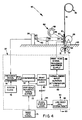
- a thermal transfer image recording system 42 which is specially configured to utilize ribbon 10 for recording a tonal image on receiving sheet 18 is diagramatically shown in FIG. 4.
- the illustrated system 42 is of the line recording type in which lines of pixel areas defining the desired image are recorded in sequence.
- Various components of system 42 are supported on a horizontal base member 43 having a paper feed through slot 44 therein.
- the recording sheet 18, in the form of plain white paper is supplied from a roll 46 supported over base member 43. From roll 46, sheet 18 passes between a pressure roller or platen 48, mounted on one side of slot 44, and laterally extending length of ribbon 10 (extending between supply and take up reels not shown) supported by a print head assembly 50 on the opposite side of slot 44. Below assembly 50, sheet 18 is fed through slot 44 and into the bite of a pair of paper advancing or line indexing rollers 51 and 52.
- Collectively, these components provide means for supporting sheet 18 in an operative position for image recording.
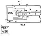
- the print head assembly 50 comprises a plate-like support 53 made of electrically insulating material.
- Support 53 has an elongated laterally extending slot or opening 54 therein defining a "window" into which the free ends of a plurality of signal electrodes 55 extend in interdigitated relationship with a plurality of corresponding spaced counter-electrodes 56.
- Each of the electrodes 55 and 56 comprises a separate electrical contact having its end opposite the free end contected to a matrix switching device 57 which is operated by a print head signal processor and power supply 58 controlled by control system 24.
- the ribbon 10 is supported on member 53 so that it overlies window 54 with the free ends of electrodes 55 and 56 in engagement with the indicator layer 16 on the back side of ribbon 10.
- the recording signal Vs is applied to the first signal electrode 55a which is paired with the first counter electrode 56x. That is, the print head signal processor 58 operates the matrix switching device 57 so that Vs is applied to electrode 55a and the counter electrode 56x is lowered to a ground potential relative to V s so that the current flow path I is established therebetween to generate heat in the corresponding section of resistive layer 14.
- signal voltage V s is applied to electrode 56b which is paired with the first counter electrode 56x.
- a dot is printed in the next adjacent pixel area C by pairing the second signal electrode 56b with the next counter electrode 56y...etc. Additional electrode pairs (not shown) are provided for the entire length of slot 54.
- the photocell detector or sensor 26 Spaced forwardly of print head assembly 50, in registration with the observation window defined by slot 54, is the photocell detector or sensor 26 for optically monitoring the density of each pixel area in the current line to be recorded.
- detector 26 comprises a linear array of photodiodes (designated 60 in FIG. 4) or the like which are equal in number and spacing to the pairs of adjacent electrodes 55 and 56 on assembly 50 for receiving reflected light from corresponding pixel area sections of layer 16 between electrodes.
- photodiodes 60 differs from those of the electrode pairs, it is preferable to provide a compensating optical component between the line of photodiodes 60 and the observation window 54 to maximize efficiency of the dot monitoring process.
- One type of commercially available detector 26 that is suitable for use in system 42 is the series G, image sensor marketed by Reticon Corp.
- the photodiode array has a pitch of about 40 diodes per mm (1000 diodes per inch). If it is used in conjunction with a print head assembly 50 that has 200 electrode pairs per inch, this means that a pixel area is 5 times larger than the photodiode area so the photodiode will not "see" the entire pixel area. This condition may be corrected by locating an objective lens 62 in the optical path which serves to provide a focused image of the larger pixel area on the small size photodiode.
- system 42 includes an illumination source 64, in the form of a lamp 66 and associated reflector 68, positioned in front of and above assembly 50 for directing light onto the strip of layer 16 registered in the observation window 54.
- an illumination source 64 in the form of a lamp 66 and associated reflector 68, positioned in front of and above assembly 50 for directing light onto the strip of layer 16 registered in the observation window 54.
- a lamp 66 such as a fluorescent lamp, that does not generate much infrared radiation to prevent overloading the photodiodes with energy outside of the visible light band that carries pixel density information.
- an optional infrared blocking filter 70 may be located in front of the photodiodes 60 to minimize erroneous readings.
- control system 24 functional components of the control system 24 are shown in block diagram form within the bounds of a dotted enclosure 24.
- a grey scale reference signal buffer memory 72 In preparation for recording a monochromatic image on sheet 18, electronic image data input signals 71 defining the pixel by pixel density of the image matrix are fed into means for receiving these signals, such as a grey scale reference signal buffer memory 72.
- the image signals are in digital form provided from an image processing computer or digital data storage device such as a disk or tape drive. If the electronic image signals were originally recorded in analog form from a video source, it is preferable that they undergo analog to digital conversion, in a manner that is well known in the art, before transmission to buffer 72.
- control system 42 may optionally include an analog to digital signal conversion subsystem for receiving analog video signals directly and converting them to digital form within control system 24.
- buffer 72 is a full frame image buffer for storing the entire image, but is also may be configured to receive portions of the image signals sequentially and for this purpose buffer 72 may comprise a smaller memory storage device for holding only one or two lines of the image.
- control system 24 includes means for receiving electronic image signals which it utilizes as grey scale reference signals that define desired or target pixel densities for comparison with observed density signals provided from the optical monitoring photodiode detector 26 in the feedback loop.
- control system 24 is coordinated with reference to a system clock 74 which among other things sets the timing for serially reading the light level or pixel density signals from each of the photodiodes 60 in the linear array.
- Light level signals from detector 26 are fed into a photodiode signal processor 76 which converts analog signals provided from detector 26 to digital form. Alternatively, this A/D conversion may take place in a subsystem incorporated into detector 26.
- Density signals from processor 76 along with reference signals from buffer 72 are fed into a signal comparator 78 which provides signals indicative of the comparison to a print decision logic system 80. Based on the comparison information, system 80 provides either a print command signal or an abort signal for each pixel in the current line. Print command signals are fed to a thermal input duration determining logic system 82, and abort signals are fed to a pixel status logic system 84.
- system 82 Upon receiving a print command, system 82 utilizing look-up tables therein to set the time period for energizing each of the electrode pairs that are to be activated and feeds this information to the print head signal processor and power supply 58 which acutates the selected electrodes in accordance with these instructions.
- the abort signals to system 84 keeps track of which pixels have been recorded and those that yet need additional thermal input for completion.
- System 84 provides an output signal to a line index and system reset system 86.
- System 86 provides a first output signal designated 90 which actuates a stepper motor (not shown) for driving the paper feed rollers 51 and 52 to advance sheet 18 one line increment in preparation for recording the next image line.
- Signal 90 also actuates another stepper motor (not shown) for driving the ribbon take-up reel to provide a fresh length of ribbon 10 over window 84.
- system 86 puts out a reset signal, designated 92, for resetting components of control system in preparation for recording the next line.
- a thermal recording cycle is initiated by actuation of the print decision logic system 80. Actuation may be accomplished by the operator manually actuating a start button (not shown).
- grey scale reference signals indicating the desired or target densities of all of the pixels in the first line are sent from buffer 72 to system 80.
- System 80 evaluates this information and for those pixel areas in which no dot is to be recorded, so as to represent the lightest tone in the grey scale, abort signals are sent to the pixel status logic system 84.
- Print command signals for those pixel areas in which a dot is to be printed are transmitted from system 80 to system 82.
- System 82 using the look-up tables, provides initial thermal input duration signals indicative of the time period that each electrode pair is to be energized to print an initial dot 36 in its corresponding pixel area PA on sheet 18 and form a corresponding indicator mark 40 in the corresponding pixel area section of layer 16.
- the initial dot be smaller than the final dot size but large enough so that the number of successive thermal energy applications needed to to make a dot of the required size is not excessive.
- system 82 will provide initial thermal input time signals to form an initial dot 36 and corresponding indicator mark 40 that is approximately 75%-85% of the final or desired dot size. This means, that each initial dot will be smaller than the pixel area in which it is formed. Even if the reference signals indicate that a high density dot which substantially fills the pixel area is to be recorded, initially a smaller dot will be formed to trigger formation an optically detectable indicator mark 40 for feedback loop utilization to achieve precise control over dot size or pixel density.
- the initial duration signals are fed from system 82 to the print head signal processor and power supply 58 which is capable of addressing each of the electrode pairs in print head assembly 50 and applying signal voltage V s thereto for the initial times indicated.
- the selected electrode pairs 55 and 56 apply voltage V s to the indicator layer 16 on the back of ribbon 10 causing heat generating current to flow in the corresponding selected sections of resistive layer 14.
- ink in sections of layer 12 corresponding to the selected pixel areas is fused and transfers to sheet 18 to form the initial dots 36 in the selected pixel area and the thermally sensitive dyes in the corresponding opposite pixel area sections of layer 16 are activated to form corresponding initial indicator dots or marks 40 that are proportional to dots 36.
- the initial indicator dots 40 are visible through the slot or window 54 and the density or reflected light level of each corresponding pixel area section PA of layer 16 between adjacent electrodes is read by the photodetector 26.
- These density signals, which are indicative of pixel density on sheet 18, are transmitted to signal processor 76 which provides the pixel density signal indications to comparator 78 for comparing the initial pixel density with the target density signals provided from reference signal buffer 72.
- Correlating the photodiode output signals to the reflective characteristics of the back side layer 16 of any particular type of ribbon 10 may be done by taking test readings on a blank ribbon 10 to establish a reference signal level for highest reflectivity which is indicative of the lowest density or brightest pixel in the grey scale.
- the setting of the reference level may be built into the recording cycle by having system 42 automatically take a photocell reading of the corresponding pixel area sections PA on layer 16 registered in the observation window 54 prior to energizing the print head to record the initial dots 36 and corresponding indicator marks 40.
- additional dot and indicator mark growth may occur subsequent to deenergization of the electrode pairs in print head assembly 50 due to residual heat attributable to the thermal inertia of the ribbon structure. Therefore, it is preferably to delay the photodetector reading for a short time after the electrode pairs are deenergized so that any additional growth will be included in this reading.
- the pixel density readings are compared to the reference signals by comparator 78 which supplies signals indicative of the difference therebetween to the print decision logic system 80. Because the initial dot size was calculated to be smaller than the final dot size the vast majority of the differential signals will indicate that additional thermal input is necessary to make each of the dots slightly larger. However, because of the variability of thermal recording parameters, at least some of the dots may have reached desired size even though the initial thermal input was intended to create a dot of only 75%-85% of desired size. For these pixels, system 80 provides abort signals to the pixel status system 84 and terminate any further thermal input thereto during the next portion of the recording cycle.
- system 80 will issue print commands to system 82 which will then provide signals indicative of the time needed to produce additional dot growth. Because the objective is now to make the dots only a little bit larger than initial size, the duration of electrode pair energization will be shorter than the times used to record the larger initial dots.
- the selected electrode pairs are energized and, following a short delay for thermal stabilization, the photodiodes 60 once again read the level of light reflected from layer 16 and feed the signals back to the comparator 78 to test these readings against the reference levels. Again, the system 80 recycles in this manner with abort signals being provided for those dots that have reached their target size and print commands being provided for pixel areas that need additional thermal input to bring their density up to target level.
- the pixel status system 84 indicates that all of the pixels in the line are at target density
- system 84 triggers the line index and reset system 86 which causes the paper to be moved one line increment; the ribbon 10 to be advanced; and various control components to be reset in preparation for recording the next image line.
- a typical line recording cycle comprises the steps of sensing the reflected light level of corresponding pixel area sections of layer 16 registered in the observation window to establish an initial reference level indicative of the lowest density pixel; in accordance with the grey scale reference signals, energizing selected electrode pairs to record initial dots in selected pixel areas which are smaller than necessary to achieve target density; following a delay to allow for additional dot growth due to heat build up and thermal inertia, sensing the reflected light level of the back side of ribbon 10 where the indicator dots 40 are formed to measure or observe the density of the initial dots; comparing the observed density with the target density; and based on this comparison initiating the application of additional thermal energy to those pixel areas which require larger dots to bring them up to target density and also terminating further input of thermal energy to those pixel areas where the comparison indicates that a predetermined comparison value has been achieved.
- the monitored density is very close to the target density, say in the range of 92 to 98% of target, it may be very difficult to tailor the next round of thermal input to that pixel area of the ribbon to achieve the very small amount of additional growth needed to reach target density. Therefore, rather than risk making the dot larger then needed to achieve an exact match with target density, it would be preferable to abort any further application of thermal energy to that particular pixel area.
- the desired dot in each pixel area is formed in steps. First an initial dot is made and the corresponding pixel area section of layer 16 is measured for comparison against the grey scale reference signal then, if necessary, one or more additional short pulses of thermal energy are sequentially applied for that pixel area to bring it up to its target density.
- dot size can be controlled to a much higher degree than if this system were to simply operate in an open loop manner with dot size being correlated to the duration of thermal energy input for each pixel area.
- system 42 may be configured for continuous power application with feedback monitoring of dot formation.
- the electrode pairs corresponding to the pixel areas PA in the line that are to have dots recorded therein in accordance with the grey scale reference signals are all turned on simultaneously.
- the indicator dots 40 appear and continue to grow, pixel density is continuously monitored and compared to the reference levels.
- the system automatically deenergizes its corresponding electrode pair. While this mode of operation may shorten the recording cycle somewhat compared to the stepwise dot formation cycle, the degree of control over dot size may not be as great because additional dot and indicator mark growth due to thermal inertia of ribbon 10 is not accounted for in the control provided by the feedback loop.
- recording system 42 has been portrayed as line recording system, this system may be modified for scanning mode operation wherein a print head assembly 50 and accompanying photodetector 26 that are narrower than a full line are moved back and forth across the width of a paper to effect image recording. Also, the print head assembly and photdetector may be configure to record on more than one line or to record the entire image so as to minimize or eliminate the need for relative movement between the components of the recording system and the thermally sensitive recording medium.
- sensing or monitoring of the indicator marks 40 is achieved with an electro-optical photodetector operating in the visible light band
- the system may be modified and employ other types of detectors which may operate at other wavelengths or may include other types of structures (for example fiber optics) to monitor recorded pixel density.
Landscapes
- Physics & Mathematics (AREA)
- Optics & Photonics (AREA)
- Impression-Transfer Materials And Handling Thereof (AREA)
- Electronic Switches (AREA)
- Thermal Transfer Or Thermal Recording In General (AREA)
- Non-Silver Salt Photosensitive Materials And Non-Silver Salt Photography (AREA)
- Transition And Organic Metals Composition Catalysts For Addition Polymerization (AREA)
- Inks, Pencil-Leads, Or Crayons (AREA)
- Adhesives Or Adhesive Processes (AREA)
Claims (11)
- Thermisch übertragendes Farbband, mit:
einer thermisch übertragbaren Tintenschicht;
einer wärmeempfindlichen und elektrisch leitfähigen Anzeigeschicht; und
einer Widerstandsschicht zum Erzeugen von Wärme in Antwort auf einen elektrischen Stromfluß in dieser Schicht, wobei diese Widerstandsschicht zwischen der Tintenschicht und der Anzeigeschicht liegt und in wärmeleitender Verbindung mit diesen beiden Schichten steht, so daß die in der Widerstandsschicht erzeugte Wärme sowohl zur Tintenschicht als auch zur Anzeigeschicht strömt, um die Tinte in der Tintenschicht zur Ausführung der Übertragung zu aktivieren und um einen entsprechenden Abschnitt der Anzeigeschicht zur Ausbildung eines optisch feststellbaren Anzeigezeichens zu aktivieren, das der Tintenübertragung von der Tintenschicht proportional ist; wobei das Farbband so ausgebildet ist, daß elektrische Signale, die an einen Abschnitt der Anzeigeschicht zwischen zwei voneinander beabstandete, mit dieser Schicht in Berührung stehende Elektroden angelegt werden, die Erzeugung von Wärme in einem Abschnitt des Farbbandes bewirken, der zwischen diesen beiden Elektroden liegt, und wobei der genannte Abschnitt der Anzeigeschicht als Anzeige arbeitet, während die beiden Elektroden mit ihm in Berührung sind. - Thermisch übertragendes Farbband nach Anspruch 1, bei welchem die Tintenschicht von der einen Seite der Widerstandsschicht und die Anzeigeschicht von der anderen Seite der Widerstandsschicht getragen ist.
- Thermisch übertragendes Farbband nach Anspruch 2, bei welchem die Tintenschicht dazu ausgebildet ist, mit einem Tintenaufnahmeblatt in Berührung gebracht zu werden, wobei die Tintenschicht von leicht schmelzbarem Typ ist, bei welchem die Tinte in Antwort auf eine Wärmezufuhr von der Widerstandsschicht schmilzt und sich auf das Aufnahmeblatt überträgt, um darauf einen Punkt zu bilden.
- Thermisch übertragendes Farbband nach Anspruch 3, bei welchem die Anzeigeschicht thermisch aktivierbare Komponenten enthält, welche in Antwort auf eine Wärmezufuhr von der Widerstandsschicht die Farbe verändern, um das genannte Anzeigezeichen zu bilden.
- Thermisch übertragendes Farbband nach Anspruch 4, bei welchem ein Punkt, der durch Übertragung von Tinte auf das Aufnahmeblatt gebildet wird, und ein entsprechendes Anzeigezeichen, das in der Anzeigeschicht gebildet wird, mit Zunahme der zur Bildung eines solchen Punktes bzw. Zeichens aufgebrachten Wärmemengen in der Größe anwachsen.
- Thermisch übertragendes Farbband nach Anspruch 1, bei welchem die Widerstandsschicht einen Polymerfilm mit darin enthaltenen leitfähigen Komponenten aufweist, um den inhärenten Widerstand des Filmes zu verringern.
- Thermisch übertragendes Farbband nach Anspruch 1, bei welchem die Anzeigeschicht ein polymeres Bindemittel enthält, auf dem ein oder mehrere wärmeempfindliche Farbstoffe und eine oder mehrere Komponenten zur Verringerung des spezifischen Widerstandes des Bindemittels dispergiert sind, um es elektrisch leitfähig zu machen.
- Thermisch übertragendes Farbband nach Anspruch 1, bei welchem die Tintenschicht auf der Vorderseite des Farbbandes liegt und dafür ausgebildet ist, mit einem Aufnahmeblatt in Berührung zu treten, um die Tintenübertragung auf dieses Blatt zu bewirken, damit ein Punkt in einer Weise gebildet wird, bei der die Punktbildung durch das Aufnahmeblatt verdeckt ist, und wobei die Anzeigeschicht auf der Rückseite des Farbbandes liegt, wo die Bildung eines Anzeigezeichens nicht verdeckt und für eine optische Erfassung sichtbar ist.
- Thermisch übertragendes Farbband nach Anspruch 1, bei welchem ein Anzeigezeichen in einem Abschnitt der Anzeigeschicht gebildet wird, der mit jenem entsprechenden gegenüberliegenden Abschnitt der Tintenschicht ausgerichtet ist, in welchem die Tinte zur Übertragung aktiviert wird.
- Thermisch übertragendes Farbband zur Verwendung mit einem thermisch übertragenden Aufzeichnungssystem zum Aufzeichnen eines Graustufenbildes auf einem Tintenaufnahmeblatt, welches System einen optischen Detektor als Teil eines Rückkopplungssystems zur Kontrolle der Größe der aufgezeichneten Punkte enthält; wobei das Farbband aufweist:
eine thermisch übertragbare Tintenschicht, die dafür ausgebildet ist, mit einem derartigen Tintenaufnahmeblatt in Berührung zu treten;
eine wärmeempfindliche und elektrisch leitfähige Anzeigeschicht; und
eine Widerstandsschicht zum Erzeugen von Wärme in Antwort auf einen elektrischen Stromfluß in dieser Schicht, wobei die Widerstandsschicht zwischen der Tintenschicht und der Anzeigeschicht liegt und in wärmeleitender Verbindung mit diesen beiden Schichten steht, so daß Wärme, die in der Widerstandsschicht erzeugt wird, sowohl zur Tintenschicht als auch zur Anzeigeschicht strömt, um die Tinte in der Tintenschicht zur Ausführung der Übertragung auf das Aufnahmeblatt zu aktivieren, wodurch ein Punkt auf diesem aufgezeichnet wird, und um einen entsprechenden Abschnitt der Anzeigeschicht zur Ausbildung eines optisch feststellbaren Anzeigezeichens darin zu aktivieren, das dem aufgezeichneten Punkt proportional und für eine Erfassung durch den Detektor des Aufzeichnungssystems zugänglich ist; wobei das Farbband so ausgebildet ist, daß elektrische Aufzeichnungssignale, die an einen Abschnitt der Anzeigeschicht zwischen zwei voneinander beabstandete, mit dieser Schicht in Berührung stehende Elektroden angelegt werden, die Erzeugung von Wärme in jenem Abschnitt des Farbbandes bewirken, welcher zwischen den beiden Elektroden liegt, und wobei der genannte Abschnitt der Anzeigeschicht als Anzeige arbeitet, während die beiden Elektroden mit ihm in Berührung stehen. - Thermisch übertragendes Farbband nach Anspruch 10, bei welchem die Tintenschicht auf einer Seite der Widerstandsschicht und die Anzeigeschicht auf der anderen Seite der Widerstandsschicht aufgebracht ist.
Priority Applications (1)
| Application Number | Priority Date | Filing Date | Title |
|---|---|---|---|
| AT86890065T ATE75187T1 (de) | 1985-03-28 | 1986-03-19 | Durch waermeuebertragung wirkendes aufzeichnungsmedium. |
Applications Claiming Priority (2)
| Application Number | Priority Date | Filing Date | Title |
|---|---|---|---|
| US06/717,122 US4603337A (en) | 1985-03-28 | 1985-03-28 | Thermal transfer recording medium |
| US717122 | 1996-09-20 |
Publications (3)
| Publication Number | Publication Date |
|---|---|
| EP0200711A2 EP0200711A2 (de) | 1986-11-05 |
| EP0200711A3 EP0200711A3 (en) | 1989-05-10 |
| EP0200711B1 true EP0200711B1 (de) | 1992-04-22 |
Family
ID=24880790
Family Applications (1)
| Application Number | Title | Priority Date | Filing Date |
|---|---|---|---|
| EP86890065A Expired - Lifetime EP0200711B1 (de) | 1985-03-28 | 1986-03-19 | Durch Wärmeübertragung wirkendes Aufzeichnungsmedium |
Country Status (6)
| Country | Link |
|---|---|
| US (1) | US4603337A (de) |
| EP (1) | EP0200711B1 (de) |
| JP (1) | JPH0635199B2 (de) |
| AT (1) | ATE75187T1 (de) |
| CA (1) | CA1260315A (de) |
| DE (2) | DE3684954D1 (de) |
Families Citing this family (8)
| Publication number | Priority date | Publication date | Assignee | Title |
|---|---|---|---|---|
| JPS6280086A (ja) * | 1985-10-02 | 1987-04-13 | Canon Inc | 印字装置 |
| US4836697A (en) * | 1988-03-21 | 1989-06-06 | Kroy Inc. | Automated thermal transfer device and control system therefor |
| JP2941037B2 (ja) * | 1989-11-02 | 1999-08-25 | キヤノン株式会社 | インクリボンカセット |
| US5126186A (en) * | 1991-06-24 | 1992-06-30 | Cheek Maurice R | Enhancement of fabric ribbon type impressions |
| FR2712842B1 (fr) * | 1993-11-24 | 1996-01-12 | Axiohm | Dispositif d'enregistrement des impressions réalisées par une imprimante thermique par transfert. |
| US5516219A (en) * | 1994-08-01 | 1996-05-14 | Lasermaster Corporation | High resolution combination donor/direct thermal printer |
| US9062575B2 (en) | 1997-10-30 | 2015-06-23 | RPM Industries, LLC | Methods and systems for performing, monitoring and analyzing multiple machine fluid processes |
| US9741515B1 (en) * | 2013-02-19 | 2017-08-22 | Amazon Technologies, Inc. | Structures for representation of an operational state |
Family Cites Families (14)
| Publication number | Priority date | Publication date | Assignee | Title |
|---|---|---|---|---|
| US3289574A (en) * | 1963-08-30 | 1966-12-06 | Cleveland Trust Co | Settable type wheel printing apparatus for a bowling game |
| JPS4826294B1 (de) * | 1968-07-20 | 1973-08-08 | ||
| CA990953A (en) * | 1972-11-30 | 1976-06-15 | Kimiaki Yoshino | Electrorecording sheet |
| JPS5413993B2 (de) * | 1973-08-17 | 1979-06-04 | ||
| NL166430C (nl) * | 1975-06-27 | 1981-08-17 | Matsushita Electric Ind Co Ltd | Werkwijze voor het witmaken van koper(i)jodide, alsmede registratievel, voorzien van elektrische geleidende lagen van aldus behandeld koper(i) jodide. |
| DE2751964C2 (de) * | 1977-11-21 | 1982-06-16 | Kraftwerk Union AG, 4330 Mülheim | Verfahren und Einrichtung zur Ermittlung von Kühlwasserleckagen an elektrischen Maschinen |
| US4195937A (en) * | 1977-09-19 | 1980-04-01 | Termcom, Inc. | Electroresistive printing apparatus |
| JPS5627366A (en) * | 1979-08-13 | 1981-03-17 | Yokogawa Hokushin Electric Corp | Recording device |
| US4291994A (en) * | 1980-03-27 | 1981-09-29 | International Business Machines Corporation | Tear resistant ribbon for non-impact printing |
| US4329071A (en) * | 1980-06-30 | 1982-05-11 | International Business Machines Corporation | Current collector for resistive ribbon printers |
| US4345845A (en) * | 1981-06-19 | 1982-08-24 | International Business Machines Corporation | Drive circuit for thermal printer |
| US4470714A (en) * | 1982-03-10 | 1984-09-11 | International Business Machines Corporation | Metal-semiconductor resistive ribbon for thermal transfer printing and method for using |
| US4477198A (en) * | 1982-06-15 | 1984-10-16 | International Business Machines Corporation | Modified resistive layer in thermal transfer medium having lubricating contact graphite coating |
| US4458253A (en) * | 1982-12-30 | 1984-07-03 | International Business Machines Corporation | Thermal print apparatus using a thermal transfer ribbon such as a multi-colored one, and a printing method |
-
1985
- 1985-03-28 US US06/717,122 patent/US4603337A/en not_active Expired - Fee Related
-
1986
- 1986-03-19 EP EP86890065A patent/EP0200711B1/de not_active Expired - Lifetime
- 1986-03-19 DE DE8686890065T patent/DE3684954D1/de not_active Expired - Fee Related
- 1986-03-19 DE DE198686890065T patent/DE200711T1/de active Pending
- 1986-03-19 CA CA000504518A patent/CA1260315A/en not_active Expired
- 1986-03-19 AT AT86890065T patent/ATE75187T1/de not_active IP Right Cessation
- 1986-03-27 JP JP61067401A patent/JPH0635199B2/ja not_active Expired - Lifetime
Also Published As
| Publication number | Publication date |
|---|---|
| EP0200711A3 (en) | 1989-05-10 |
| EP0200711A2 (de) | 1986-11-05 |
| JPH0635199B2 (ja) | 1994-05-11 |
| DE200711T1 (de) | 1987-03-19 |
| DE3684954D1 (de) | 1992-05-27 |
| CA1260315A (en) | 1989-09-26 |
| ATE75187T1 (de) | 1992-05-15 |
| JPS61227081A (ja) | 1986-10-09 |
| US4603337A (en) | 1986-07-29 |
Similar Documents
| Publication | Publication Date | Title |
|---|---|---|
| EP0203056B1 (de) | Thermalübertragungsfarbwiedergabegerät und Band | |
| EP0186651B1 (de) | Anordnung und Verfahren zur thermischen Aufzeichnung | |
| US5534890A (en) | Thermal printer for printing labels | |
| EP0468237B1 (de) | Verfahren und Vorrichtung für die wiedereinschreibbare und löschbare Aufzeichnung und wiedereinschreibbarer Aufzeichnungsfilm | |
| EP0183680B1 (de) | Verfahren und Vorrichtung zur thermalen Aufzeichnung | |
| US8708447B2 (en) | Temperature monitoring system for a media preheater | |
| US5796420A (en) | Method for correcting across-the-head uneveness in a thermal printing system | |
| EP0200711B1 (de) | Durch Wärmeübertragung wirkendes Aufzeichnungsmedium | |
| EP0187133B1 (de) | Wärmeempfindliches Aufzeichnungsmaterial und Verfahren | |
| EP0198813B1 (de) | Verfahren und Anordnung zur Aufzeichnung durch Wärmeübertragung | |
| US5896159A (en) | Temperature controlling method and apparatus for a thermal printhead | |
| EP0627319B1 (de) | Verfahren zum Korrigieren der Ungleichmässigkeit in einem Thermodrucksystem | |
| JPS63147668A (ja) | 感熱記録装置 | |
| JP2000094792A (ja) | 情報消去装置、情報記録・消去装置および、これらにおける情報の誤消去防止方法 | |
| JPH0220379A (ja) | リボン残量検知方法 | |
| JPH0532009A (ja) | 記録装置 |
Legal Events
| Date | Code | Title | Description |
|---|---|---|---|
| PUAI | Public reference made under article 153(3) epc to a published international application that has entered the european phase |
Free format text: ORIGINAL CODE: 0009012 |
|
| ITCL | It: translation for ep claims filed |
Representative=s name: RICCARDI SERGIO & CO. |
|
| AK | Designated contracting states |
Kind code of ref document: A2 Designated state(s): AT CH DE FR GB IT LI NL |
|
| PUAB | Information related to the publication of an a document modified or deleted |
Free format text: ORIGINAL CODE: 0009199EPPU |
|
| EL | Fr: translation of claims filed | ||
| TCAT | At: translation of patent claims filed | ||
| TCNL | Nl: translation of patent claims filed | ||
| RA1 | Application published (corrected) |
Date of ref document: 19861210 Kind code of ref document: A2 |
|
| DET | De: translation of patent claims | ||
| PUAL | Search report despatched |
Free format text: ORIGINAL CODE: 0009013 |
|
| AK | Designated contracting states |
Kind code of ref document: A3 Designated state(s): AT CH DE FR GB IT LI NL |
|
| 17P | Request for examination filed |
Effective date: 19891014 |
|
| 17Q | First examination report despatched |
Effective date: 19910605 |
|
| GRAA | (expected) grant |
Free format text: ORIGINAL CODE: 0009210 |
|
| STAA | Information on the status of an ep patent application or granted ep patent |
Free format text: STATUS: THE PATENT HAS BEEN GRANTED |
|
| AK | Designated contracting states |
Kind code of ref document: B1 Designated state(s): AT CH DE FR GB IT LI NL |
|
| REF | Corresponds to: |
Ref document number: 75187 Country of ref document: AT Date of ref document: 19920515 Kind code of ref document: T |
|
| ET | Fr: translation filed | ||
| REF | Corresponds to: |
Ref document number: 3684954 Country of ref document: DE Date of ref document: 19920527 |
|
| ITF | It: translation for a ep patent filed |
Owner name: UFFICIO BREVETTI RICCARDI & C. |
|
| PLBE | No opposition filed within time limit |
Free format text: ORIGINAL CODE: 0009261 |
|
| PG25 | Lapsed in a contracting state [announced via postgrant information from national office to epo] |
Ref country code: AT Effective date: 19930319 |
|
| PG25 | Lapsed in a contracting state [announced via postgrant information from national office to epo] |
Ref country code: LI Effective date: 19930331 Ref country code: CH Effective date: 19930331 |
|
| 26N | No opposition filed | ||
| REG | Reference to a national code |
Ref country code: CH Ref legal event code: PL |
|
| PGFP | Annual fee paid to national office [announced via postgrant information from national office to epo] |
Ref country code: FR Payment date: 19970210 Year of fee payment: 12 |
|
| PGFP | Annual fee paid to national office [announced via postgrant information from national office to epo] |
Ref country code: GB Payment date: 19970220 Year of fee payment: 12 |
|
| PGFP | Annual fee paid to national office [announced via postgrant information from national office to epo] |
Ref country code: DE Payment date: 19970224 Year of fee payment: 12 |
|
| PGFP | Annual fee paid to national office [announced via postgrant information from national office to epo] |
Ref country code: NL Payment date: 19970225 Year of fee payment: 12 |
|
| PG25 | Lapsed in a contracting state [announced via postgrant information from national office to epo] |
Ref country code: GB Free format text: LAPSE BECAUSE OF NON-PAYMENT OF DUE FEES Effective date: 19980319 |
|
| PG25 | Lapsed in a contracting state [announced via postgrant information from national office to epo] |
Ref country code: FR Free format text: THE PATENT HAS BEEN ANNULLED BY A DECISION OF A NATIONAL AUTHORITY Effective date: 19980331 |
|
| PG25 | Lapsed in a contracting state [announced via postgrant information from national office to epo] |
Ref country code: NL Free format text: LAPSE BECAUSE OF NON-PAYMENT OF DUE FEES Effective date: 19981001 |
|
| GBPC | Gb: european patent ceased through non-payment of renewal fee |
Effective date: 19980319 |
|
| NLV4 | Nl: lapsed or anulled due to non-payment of the annual fee |
Effective date: 19981001 |
|
| PG25 | Lapsed in a contracting state [announced via postgrant information from national office to epo] |
Ref country code: DE Free format text: LAPSE BECAUSE OF NON-PAYMENT OF DUE FEES Effective date: 19981201 |
|
| REG | Reference to a national code |
Ref country code: FR Ref legal event code: ST |
|
| PG25 | Lapsed in a contracting state [announced via postgrant information from national office to epo] |
Ref country code: IT Free format text: LAPSE BECAUSE OF NON-PAYMENT OF DUE FEES;WARNING: LAPSES OF ITALIAN PATENTS WITH EFFECTIVE DATE BEFORE 2007 MAY HAVE OCCURRED AT ANY TIME BEFORE 2007. THE CORRECT EFFECTIVE DATE MAY BE DIFFERENT FROM THE ONE RECORDED. Effective date: 20050319 |