EP0200452B1 - Light-transmissible plate shielding electromagnetic waves - Google Patents
Light-transmissible plate shielding electromagnetic waves Download PDFInfo
- Publication number
- EP0200452B1 EP0200452B1 EP86302982A EP86302982A EP0200452B1 EP 0200452 B1 EP0200452 B1 EP 0200452B1 EP 86302982 A EP86302982 A EP 86302982A EP 86302982 A EP86302982 A EP 86302982A EP 0200452 B1 EP0200452 B1 EP 0200452B1
- Authority
- EP
- European Patent Office
- Prior art keywords
- layer
- light
- plate
- hard coating
- base plate
- Prior art date
- Legal status (The legal status is an assumption and is not a legal conclusion. Google has not performed a legal analysis and makes no representation as to the accuracy of the status listed.)
- Expired - Lifetime
Links
- 239000010410 layer Substances 0.000 claims description 224
- 239000011247 coating layer Substances 0.000 claims description 69
- 239000010408 film Substances 0.000 claims description 54
- VYPSYNLAJGMNEJ-UHFFFAOYSA-N Silicium dioxide Chemical compound O=[Si]=O VYPSYNLAJGMNEJ-UHFFFAOYSA-N 0.000 claims description 50
- 229920003023 plastic Polymers 0.000 claims description 43
- 238000000034 method Methods 0.000 claims description 34
- 238000000576 coating method Methods 0.000 claims description 29
- 239000011248 coating agent Substances 0.000 claims description 25
- 239000000377 silicon dioxide Substances 0.000 claims description 25
- 239000004615 ingredient Substances 0.000 claims description 16
- 235000012239 silicon dioxide Nutrition 0.000 claims description 16
- 239000006117 anti-reflective coating Substances 0.000 claims description 12
- 239000003973 paint Substances 0.000 claims description 10
- 238000004544 sputter deposition Methods 0.000 claims description 9
- XOLBLPGZBRYERU-UHFFFAOYSA-N tin dioxide Chemical compound O=[Sn]=O XOLBLPGZBRYERU-UHFFFAOYSA-N 0.000 claims description 9
- 238000007738 vacuum evaporation Methods 0.000 claims description 9
- GWEVSGVZZGPLCZ-UHFFFAOYSA-N Titan oxide Chemical compound O=[Ti]=O GWEVSGVZZGPLCZ-UHFFFAOYSA-N 0.000 claims description 8
- 230000003287 optical effect Effects 0.000 claims description 8
- 239000012788 optical film Substances 0.000 claims description 8
- 229910003437 indium oxide Inorganic materials 0.000 claims description 7
- PJXISJQVUVHSOJ-UHFFFAOYSA-N indium(iii) oxide Chemical compound [O-2].[O-2].[O-2].[In+3].[In+3] PJXISJQVUVHSOJ-UHFFFAOYSA-N 0.000 claims description 7
- 239000012298 atmosphere Substances 0.000 claims description 6
- 238000001704 evaporation Methods 0.000 claims description 6
- 230000008020 evaporation Effects 0.000 claims description 6
- OGIDPMRJRNCKJF-UHFFFAOYSA-N titanium oxide Inorganic materials [Ti]=O OGIDPMRJRNCKJF-UHFFFAOYSA-N 0.000 claims description 6
- QVGXLLKOCUKJST-UHFFFAOYSA-N atomic oxygen Chemical compound [O] QVGXLLKOCUKJST-UHFFFAOYSA-N 0.000 claims description 5
- 238000013461 design Methods 0.000 claims description 5
- 238000010894 electron beam technology Methods 0.000 claims description 5
- 239000001301 oxygen Substances 0.000 claims description 5
- 229910052760 oxygen Inorganic materials 0.000 claims description 5
- RVTZCBVAJQQJTK-UHFFFAOYSA-N oxygen(2-);zirconium(4+) Chemical compound [O-2].[O-2].[Zr+4] RVTZCBVAJQQJTK-UHFFFAOYSA-N 0.000 claims description 5
- 229910001887 tin oxide Inorganic materials 0.000 claims description 5
- 229910001928 zirconium oxide Inorganic materials 0.000 claims description 5
- 230000005540 biological transmission Effects 0.000 claims description 4
- 150000002500 ions Chemical class 0.000 claims description 4
- 239000012790 adhesive layer Substances 0.000 claims 6
- 229920001296 polysiloxane Polymers 0.000 claims 2
- 238000001771 vacuum deposition Methods 0.000 claims 1
- 239000004033 plastic Substances 0.000 description 14
- 229910052751 metal Inorganic materials 0.000 description 12
- 239000002184 metal Substances 0.000 description 12
- 239000000203 mixture Substances 0.000 description 10
- 230000003068 static effect Effects 0.000 description 8
- 239000000463 material Substances 0.000 description 7
- -1 polyorganosiloxane Substances 0.000 description 7
- QTBSBXVTEAMEQO-UHFFFAOYSA-N Acetic acid Chemical compound CC(O)=O QTBSBXVTEAMEQO-UHFFFAOYSA-N 0.000 description 6
- 238000005299 abrasion Methods 0.000 description 5
- 150000001875 compounds Chemical class 0.000 description 5
- 238000005516 engineering process Methods 0.000 description 5
- XKRFYHLGVUSROY-UHFFFAOYSA-N Argon Chemical compound [Ar] XKRFYHLGVUSROY-UHFFFAOYSA-N 0.000 description 4
- PNEYBMLMFCGWSK-UHFFFAOYSA-N aluminium oxide Inorganic materials [O-2].[O-2].[O-2].[Al+3].[Al+3] PNEYBMLMFCGWSK-UHFFFAOYSA-N 0.000 description 4
- 230000005611 electricity Effects 0.000 description 4
- 239000011521 glass Substances 0.000 description 4
- 230000003301 hydrolyzing effect Effects 0.000 description 4
- XLYOFNOQVPJJNP-UHFFFAOYSA-N water Substances O XLYOFNOQVPJJNP-UHFFFAOYSA-N 0.000 description 4
- 229920006353 Acrylite® Polymers 0.000 description 3
- 230000001133 acceleration Effects 0.000 description 3
- 229960000583 acetic acid Drugs 0.000 description 3
- FWDBOZPQNFPOLF-UHFFFAOYSA-N ethenyl(triethoxy)silane Chemical compound CCO[Si](OCC)(OCC)C=C FWDBOZPQNFPOLF-UHFFFAOYSA-N 0.000 description 3
- 239000004744 fabric Substances 0.000 description 3
- 239000000835 fiber Substances 0.000 description 3
- 239000012362 glacial acetic acid Substances 0.000 description 3
- 238000010884 ion-beam technique Methods 0.000 description 3
- 238000005259 measurement Methods 0.000 description 3
- 229920000193 polymethacrylate Polymers 0.000 description 3
- 239000004926 polymethyl methacrylate Substances 0.000 description 3
- LYCAIKOWRPUZTN-UHFFFAOYSA-N Ethylene glycol Chemical compound OCCO LYCAIKOWRPUZTN-UHFFFAOYSA-N 0.000 description 2
- PEDCQBHIVMGVHV-UHFFFAOYSA-N Glycerine Chemical compound OCC(O)CO PEDCQBHIVMGVHV-UHFFFAOYSA-N 0.000 description 2
- 229920000297 Rayon Polymers 0.000 description 2
- VMHLLURERBWHNL-UHFFFAOYSA-M Sodium acetate Chemical compound [Na+].CC([O-])=O VMHLLURERBWHNL-UHFFFAOYSA-M 0.000 description 2
- NIXOWILDQLNWCW-UHFFFAOYSA-N acrylic acid group Chemical group C(C=C)(=O)O NIXOWILDQLNWCW-UHFFFAOYSA-N 0.000 description 2
- 229910052786 argon Inorganic materials 0.000 description 2
- 229910052681 coesite Inorganic materials 0.000 description 2
- 229910052906 cristobalite Inorganic materials 0.000 description 2
- 230000002939 deleterious effect Effects 0.000 description 2
- 230000000694 effects Effects 0.000 description 2
- 238000005421 electrostatic potential Methods 0.000 description 2
- 238000005530 etching Methods 0.000 description 2
- 238000003475 lamination Methods 0.000 description 2
- 239000000314 lubricant Substances 0.000 description 2
- 238000001755 magnetron sputter deposition Methods 0.000 description 2
- 239000004848 polyfunctional curative Substances 0.000 description 2
- 239000002964 rayon Substances 0.000 description 2
- 230000035939 shock Effects 0.000 description 2
- 229910052710 silicon Inorganic materials 0.000 description 2
- 239000010703 silicon Substances 0.000 description 2
- 239000001632 sodium acetate Substances 0.000 description 2
- 235000017281 sodium acetate Nutrition 0.000 description 2
- 229910052682 stishovite Inorganic materials 0.000 description 2
- 229910052905 tridymite Inorganic materials 0.000 description 2
- CPUDPFPXCZDNGI-UHFFFAOYSA-N triethoxy(methyl)silane Chemical compound CCO[Si](C)(OCC)OCC CPUDPFPXCZDNGI-UHFFFAOYSA-N 0.000 description 2
- OKTJSMMVPCPJKN-UHFFFAOYSA-N Carbon Chemical compound [C] OKTJSMMVPCPJKN-UHFFFAOYSA-N 0.000 description 1
- RYGMFSIKBFXOCR-UHFFFAOYSA-N Copper Chemical compound [Cu] RYGMFSIKBFXOCR-UHFFFAOYSA-N 0.000 description 1
- LFQSCWFLJHTTHZ-UHFFFAOYSA-N Ethanol Chemical compound CCO LFQSCWFLJHTTHZ-UHFFFAOYSA-N 0.000 description 1
- CERQOIWHTDAKMF-UHFFFAOYSA-N Methacrylic acid Chemical compound CC(=C)C(O)=O CERQOIWHTDAKMF-UHFFFAOYSA-N 0.000 description 1
- 229910001128 Sn alloy Inorganic materials 0.000 description 1
- AZWHFTKIBIQKCA-UHFFFAOYSA-N [Sn+2]=O.[O-2].[In+3] Chemical compound [Sn+2]=O.[O-2].[In+3] AZWHFTKIBIQKCA-UHFFFAOYSA-N 0.000 description 1
- 235000011054 acetic acid Nutrition 0.000 description 1
- 125000000218 acetic acid group Chemical class C(C)(=O)* 0.000 description 1
- 238000004458 analytical method Methods 0.000 description 1
- 230000003667 anti-reflective effect Effects 0.000 description 1
- 239000012300 argon atmosphere Substances 0.000 description 1
- 239000011230 binding agent Substances 0.000 description 1
- 229910052799 carbon Inorganic materials 0.000 description 1
- 238000004140 cleaning Methods 0.000 description 1
- 229910052802 copper Inorganic materials 0.000 description 1
- 239000010949 copper Substances 0.000 description 1
- 238000005336 cracking Methods 0.000 description 1
- 238000007598 dipping method Methods 0.000 description 1
- 238000004043 dyeing Methods 0.000 description 1
- 239000003822 epoxy resin Substances 0.000 description 1
- 150000002148 esters Chemical class 0.000 description 1
- 239000007789 gas Substances 0.000 description 1
- 235000011187 glycerol Nutrition 0.000 description 1
- 238000010438 heat treatment Methods 0.000 description 1
- 230000007062 hydrolysis Effects 0.000 description 1
- 238000006460 hydrolysis reaction Methods 0.000 description 1
- WGCNASOHLSPBMP-UHFFFAOYSA-N hydroxyacetaldehyde Natural products OCC=O WGCNASOHLSPBMP-UHFFFAOYSA-N 0.000 description 1
- RHZWSUVWRRXEJF-UHFFFAOYSA-N indium tin Chemical compound [In].[Sn] RHZWSUVWRRXEJF-UHFFFAOYSA-N 0.000 description 1
- 229910010272 inorganic material Inorganic materials 0.000 description 1
- 239000011147 inorganic material Substances 0.000 description 1
- 238000004519 manufacturing process Methods 0.000 description 1
- BFXIKLCIZHOAAZ-UHFFFAOYSA-N methyltrimethoxysilane Chemical compound CO[Si](C)(OC)OC BFXIKLCIZHOAAZ-UHFFFAOYSA-N 0.000 description 1
- 238000012856 packing Methods 0.000 description 1
- 238000005192 partition Methods 0.000 description 1
- WXZMFSXDPGVJKK-UHFFFAOYSA-N pentaerythritol Chemical compound OCC(CO)(CO)CO WXZMFSXDPGVJKK-UHFFFAOYSA-N 0.000 description 1
- 230000000704 physical effect Effects 0.000 description 1
- 229920000647 polyepoxide Polymers 0.000 description 1
- 229920000728 polyester Polymers 0.000 description 1
- 238000005070 sampling Methods 0.000 description 1
- 238000002798 spectrophotometry method Methods 0.000 description 1
- 239000000126 substance Substances 0.000 description 1
- 239000002344 surface layer Substances 0.000 description 1
- PBCFLUZVCVVTBY-UHFFFAOYSA-N tantalum pentoxide Inorganic materials O=[Ta](=O)O[Ta](=O)=O PBCFLUZVCVVTBY-UHFFFAOYSA-N 0.000 description 1
- 238000012360 testing method Methods 0.000 description 1
- 238000002834 transmittance Methods 0.000 description 1
- 238000009941 weaving Methods 0.000 description 1
Images

Classifications
-
- H—ELECTRICITY
- H01—ELECTRIC ELEMENTS
- H01J—ELECTRIC DISCHARGE TUBES OR DISCHARGE LAMPS
- H01J29/00—Details of cathode-ray tubes or of electron-beam tubes of the types covered by group H01J31/00
- H01J29/86—Vessels; Containers; Vacuum locks
- H01J29/89—Optical or photographic arrangements structurally combined or co-operating with the vessel
- H01J29/896—Anti-reflection means, e.g. eliminating glare due to ambient light
-
- H—ELECTRICITY
- H01—ELECTRIC ELEMENTS
- H01J—ELECTRIC DISCHARGE TUBES OR DISCHARGE LAMPS
- H01J29/00—Details of cathode-ray tubes or of electron-beam tubes of the types covered by group H01J31/00
- H01J29/86—Vessels; Containers; Vacuum locks
- H01J29/867—Means associated with the outside of the vessel for shielding, e.g. magnetic shields
- H01J29/868—Screens covering the input or output face of the vessel, e.g. transparent anti-static coatings, X-ray absorbing layers
-
- H—ELECTRICITY
- H01—ELECTRIC ELEMENTS
- H01J—ELECTRIC DISCHARGE TUBES OR DISCHARGE LAMPS
- H01J2229/00—Details of cathode ray tubes or electron beam tubes
- H01J2229/89—Optical components associated with the vessel
- H01J2229/8913—Anti-reflection, anti-glare, viewing angle and contrast improving treatments or devices
- H01J2229/8918—Anti-reflection, anti-glare, viewing angle and contrast improving treatments or devices by using interference effects
-
- H—ELECTRICITY
- H01—ELECTRIC ELEMENTS
- H01J—ELECTRIC DISCHARGE TUBES OR DISCHARGE LAMPS
- H01J2229/00—Details of cathode ray tubes or electron beam tubes
- H01J2229/89—Optical components associated with the vessel
- H01J2229/8913—Anti-reflection, anti-glare, viewing angle and contrast improving treatments or devices
- H01J2229/8922—Apparatus attached to vessel and not integral therewith
Definitions
- the present invention relates to a light-transmissible plastic plate which shields electromagnetic waves. More particularly, the present invention relates to a light-transmissible plate capable of effectively shielding deleterious electromagnetic waves which are generated from a display or a Braun tube etc. Moreover, the present invention relates to a light-transmissible plate having durability and the function of reducing reflection.
- One of the improvements is a method of covering the equipment which generates electromagnetic waves with electroconductive material such as a metal.
- a cloth capable of shielding electromagnetic waves and an "Eyesaver” (the trade name of a product of Chori Kabushiki Kaisha, a Japanese company) are known.
- the cloth is constructed by adhering carbon onto a fiber with small diameter and then weaving the fiber to form a meshed structure, and the cloth is applied on equipment which generates electromagnetic waves.
- "Eyesaver” is constructed of glass sheets and metal wire positioned between the sheets.
- a method of forming an evaporation coating layer of electroconductive material on a glass plate is also known. Such a method is disclosed, for example, in Japanese Patent Publication No. SHO 49-18447.
- GB-A-2121075 discloses a method of forming a heatwave shielding lamination coating of electroconductive material on a glass window using the DC magnetron sputtering method. In this method a car window pane is heated to 370°C in an atmosphere at a pressure of 3 x 10 ⁇ 3 Torr.
- the lamination coating includes layers of the same refractive index at visible wavelengths but different refractive indices at infrared wavelengths.
- the base plate is liable to soften or to melt, and is liable to be damaged at the surface. Therefore, the method cannot be applied for manufacturing a light-transmissible plastic plate.
- US-A-4422721 describes the application to glass of anti-reflection coatings each comprising a layer of low refractive index carrying an electroconductive layer of high refractive index.
- EP-A-0145210 describes anti-reflection optical coatings provided on an anti-reflective panel of unspecified material and bonded to the viewing screen of a cathode ray tube.
- the anti-reflection optical coatings each include an electroconductive layer and a free surface layer of a material having a refractive index lower than that of the electroconductive layer.
- SHO 59-48702, SHO 59-78301 and SHO 59-78304 disclose a method of providing anti-reflection coatings wherein a hard coating film comprising a polyorganosilane or a hardened film comprising an epoxy resin is formed on a plastic base plate and then an anti-reflection film comprising inorganic material is coated on the above hard coating layer.
- Japanese Patent Publication No. SHO 56-113101 discloses a structure wherein an anti-reflection film comprising a plurality of oxide compound layers is provided on a plastic base plate. The structure has high hardness at the surface and a satisfactory anti-reflection function, but adhesion between the base plate and the film, heat resistance, shock resistance, hot water resistance and weather resistance thereof are not satisfactory.
- Japanese Patent Publication Nos. SHO 45-6193, SHO 59-48702, SHO 59-78301 and SHO 59-78304 disclose other structures including other anti-reflection films, but the adhesion between the base plate and the anti-reflection film in these structures is also unsatisfactory, and the surfaces of anti-reflection films are liable to be damaged. Moreover, the plates are liable to be damaged by water or alcohol, and the structures have adhesion problems between the base plate and the film after dipping the plate into hot water and also in severe weather.
- the present invention seeks to provide a light-transmissible plate which can shield electromagnetic waves wherein an electroconductive layer is coated on a base plate, even if the base plate is constructed of a plastic material.
- the present invention in one of its aspects also seeks to provide a technology wherein hardness at a surface of the light-transmissible plate can be increased.
- the invention seeks to provide a technology wherein the light-transmissible plate can also have a function of anti-reflection.
- the present invention seeks to provide a light-transmissible plate which includes an anti-reflection film having excellent physical properties in various respects.
- a light-transmissible plate capable of transmitting visible light and yet shielding electromagnetic waves generated by electronic equipment and having: a transparent plastic base plate; on a surface of the transparent base plate, a first hard coating layer having scratch resistance; on a surface of the hard coating layer remote from the transparent plastic base plate, an electroconductive layer, which electroconductive layer contains indium oxide and tin oxide; on a surface of the electroconductive layer remote from the transparent plastic base plate, a layer having a refractive index in the visible light region which is lower than that of said electroconductive layer; on a surface of the transparent plastic base plate which is to face a viewer, a second hard coating layer; and on a surface of the second hard coating layer remote from the transparent plastic base plate, an antireflective coating, which antireflective coating consists of a plurality of layers, wherein the first hard coating layer on which is disposed the electroconductive layer is disposed on a surface of the transparent base plate which is to face the source of visible light, being opposite to the surface
- the invention provides (i) an electronic device having a source of visible light and including the above light transmissible plate, and (ii) the use, for the transmission of light from a light source of an electronic device while at the same time shielding electromagnetic waves from the electronic device, of the above light transmissible plate.
- the invention provides a method of preparing the above plate, which method comprises the steps of
- FIG. 1 is a sectional view of a light-transmissible plate having the function of shielding electromagnetic waves and the function of resisting static charge according to one embodiment of the present invention.
- Hard coating layer 2 is provided on one surface of the transparent base plate 1, and the hard coating layer 2 has scratch resistance.
- Electroconductive layer 3 is provided on a surface of the hard coating layer 2.
- Layer 4 is provided on a surface of the electroconductive layer 3, and layer 4 has a lower refractive index than the refractive index of the electroconductive layer 3.
- Numeral 5 refers to a portion of an exposed surface of electroconductive layer 3.
- Light-transmissible plate 100 is disposed so as to direct a surface having electroconductive layer 3 toward a surface generating picture image, for example, a surface of a cathode-ray tube.
- FIG. 2 is a plan view of the light-transmissible plate 100 in FIG. 1.
- Exposed surface 5 of electroconductive layer 3 may be formed either along the entire periphery of the light-transmissible plate 100, or along only a part of the periphery.
- a metal frame (not shown) is provided around the plate 100 so as to contact with electroconductive layer 3, or an earthing wire 6 is connected to the electroconductive layer 3.
- the earthing wire 6 is connected desirably to a corner of electroconductive layer 3.
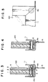
- FIG. 3 - 7 show preferred embodiments according to the present invention in relation to connecting an earthing wire.
- hole 9 is provided through the light-transmissible plate 100, and an earthing wire 15 is connected thereto via metal fitting piece 6a.
- metal fitting piece 6a is fixed by a fixing means, for example, set screw 10a and nut 10b (FIG.3), or a caulking piece 8 (FIG. 4). Then the portion of the connection is covered by a plastic cover 11.
- FIG. 5 shows an embodiment wherein metal fitting piece 6a is fixed nearly parallel to light-transmissible plate 100 in plastic cover 11.
- FIG. 6 shows an embodiment wherein helical insert 12 is fitted into hole 9 and earthing wire 15 is fixed by screw 13 via metal fitting piece 6a.
- providing a hole 11a on the cover 11 facilitates removing the screw 13, and the structure is convenient for removing light-transmissible plate 100 from equipment or cleaning the plate 100.
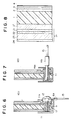
- FIG. 7 shows an embodiment wherein earthing wire 15 is connected to the plate 100 via adjuster 14a and 14b.
- FIG. 8 is a partial sectional view of a light-transmissible plate having an anti-reflection film constituted by a plurality of layers according to a second embodiment of the present invention.
- hard coating layer 2 On one surface of transparent plastic base plate 1, hard coating layer 2, electroconductive layer 3 and layer 4 having a lower refractive index than the refractive index of electroconductive layer 3 are provided, and on another surface of base plate 1, hard coating layer 2' having scratch resistance and anti-reflection film 20 are provided.
- Anti-reflection film 20 is constructed of No. 1 layer 21, No. 2 layer 22, No. 3 layer 23 and No. 4 layer 24.
- a first hard coating layer having scratch resistance is provided on a first surface of a transparent plastic base plate.
- a plastic constituting the base plate may be any conventional plastic.
- the transparent base plate means any plastic plate capable of transmitting light. In the case where a light-transmissible plate is used for a display of a word processor etc., it is desirable to apply a base plate set to the transmittance of visible rays of 25 - 70% by its own color or dyeing. Fatigue of the eyes of an operator is reduced by the above restriction.
- the hard coating layer having scratch resistance means a coating layer having high hardness, for example, a layer including polyorganosiloxane, silica or alumina, or a coating layer constructed of a hardening paint, for example, an acrylic paint.
- the hard coating layer consists of a polyorganosiloxane which is produced by heat-condensing after coating methyltrimethoxysilane and vinyltriethoxysilane or after coating a hydrolysis compound thereof.
- a desirable film thickness of the hard coating layer is in the range of about 1 - 10 ⁇ m.
- the hard coating layer including the acrylic is constructed of, for example, a compound crosslinked with an acrylic compound and an ester compound.
- the acrylic compound is constructed of, for example, methacrylic acid and the ester compound is constructed of, for example, an ester compound produced from an ester and a polyfunctional glycol, for example, pentaerythritol or glycerin.
- an electroconductive layer is provided on a surface of the hard coating layer.
- Any material having electroconductivity and capable of transmitting light can be used for the electroconductive layer, but preferably the layer is constructed of a mixture with indium oxide (In2O3) and tin oxide (SnO2), referred to hereinafter as "ITO".
- ITO has high electroconductivity, can shield electromagnetic waves effectively and can transmit visible rays.
- a film thickness of the "ITO” layer may be any thickness as long as the layer can satisfy the above functions.
- a desirable thickness is in the range of 100 - 3000 ⁇ (10-300nm) If a thickness of more than 300 nm is utilized, cracking is liable to occur.
- the "ITO” layer can be coated by sputtering.
- the "ITO” layer is formed by evaporation coating using plasma due to high-frequency electric discharge in an atmosphere of oxygen and in a temperature condition of less than 150°C, with the assistance of an ion gun.
- a layer having a lower refractive index than the refractive index of the electroconductive layer is provided on the surface of the electroconductive layer.
- the refractive index of the layer is high.
- the refractive index of the "ITO" layer is about 2.0.
- the layer having a low refractive index may be any conventional layer of low refractive index, but desirably the layer is a layer including inorganic silica.
- the layer including inorganic silica can be formed by sputtering the silica or by vacuum evaporation coating of the silica.
- the film thickness of the layer may be any thickness as long as the layer can appropriately prevent reflection.
- the first hard coating layer, the electroconductive layer and the layer having the low refractive index are provided on the first surface of the base plate, while on a second surface of the base plate opposite the first surface at least a second hard coating layer is provided and on this second hard coating layer an anti-reflection coating is provided.
- the anti-reflection coating is a film composed of a plurality of layers which in turn may be referred to as a No. 1 layer, No. 2 layer, No. 3 layer and a No. 4 layer.
- the No. 1 layer is provided on the surface of the second hard coating layer.
- the principal ingredient of the No. 1 layer is zirconium oxide.
- the No. 2 layer is provided on the surface of the No. 1 layer, and the principal ingredient of the No. 2 layer is silicon dioxide.
- the No. 1 layer serves as a binder between the hard coating layer and the No. 2 layer, and the strength of both adhesions between the hard coating layer and the No. 1 layer and between the No. 1 layer and the No. 2 layer is increased.
- the No. 1 layer serves as a binder between the hard coating layer and the No. 2 layer, and the strength of both adhesions between the hard coating layer and the No. 1 layer and between the No. 1 layer and the No. 2 layer is increased.
- the No. 1 layer serves as
- the equivalent film can be a film having a middle refractive index, ie a refractive index between that of the No. 3 layer having a high refractive index and that of the No. 4 layer having a low refractive index.
- the No. 3 layer is provided on a surface of the No. 2 layer, and the principal ingredient of the No. 3 layer is titanium oxide.
- the No. 4 layer is provided on a surface of the No. 3 layer, and the principal ingredient of the No. 4 layer is silicon dioxide.
- the film equivalent to No. 1 layer and No. 2 layer and having the middle refractive index, the No. 3 layer having the high index and the No. 4 layer having the low index, constitute the anti-reflection film as a whole, with the film having the excellent function of preventing reflection.
- the above anti-reflection film can be coated by vacuum evaporation or sputtering. Vacuum evaporation is better than sputtering. The assistance of an ion beam may be utilized for forming the film. Titanium oxide can be added into the No. 1 layer including zirconium oxide as long as the effect desired for a light transmissible plate of the present invention is not reduced. In the same manner, Ta2O5 can be added to the No. 3 layer including titanium oxide.
- the thickness of the anti-reflection film may be any thickness as long as the film can prevent the reflection of visible rays.
- Preferable optical film thicknesses are as follows when the design wave length ⁇ 0 is within 450 - 550 nm. No. 1 layer; 0.05 - 0.15 ⁇ 0, No. 2 layer; 0.05 - 0.15 ⁇ 0, No. 3 layer; 0.36 - 0.49 ⁇ 0, and No. 4 layer; 0.15 - 0.35 ⁇ 0.
- the thickness of No. 4 layer is desirably 0.25 ⁇ 0.
- the anti-reflection film constructed of a plurality of layers is provided on one surface of the plastic base plate, while the indium oxide-tin oxide layer ("ITO" layer) and the layer including silicon dioxide are provided on the opposite surface.
- ITO indium oxide-tin oxide layer
- a layer having the function of preventing reflection is formed on one surface and a layer having the function of shielding electromagnetic waves is formed on the opposite surface.
- the film thickness of the "ITO” layer is formed to a large size relatively, for example, 500 - 1000 ⁇ (50-100nm).
- an earthing means may be connected thereto to eliminate static electricity.
- an earthing wire may be connected to the "ITO” layer directly, or continuity via a particular electroconductive component between the "ITO” layer and the earthing wire may be ensured.
- an outer frame constructed of metal may be provided around the plate, and static electricity may be discharged via the frame.
- the metal frame may preferably come into contact with the "ITO” layer directly, or continuity via a particular electroconductive component between the metal frame and "ITO" layer may be maintained.
- providing the hard coating layer on the transparent plastic base plate can raise the hardness of the light-transmissible plate, thereby providing characteristics of abrasion resistance and wear resistance to the plate, even if the base plate consists of a plastic having low hardness.
- Providing the electroconductive layer formed on the hard coating layer and the layer having a low refractive index formed on the electroconductive layer can shield electromagnetic waves, and at the same time can prevent reflection.
- an anti-reflection film having excellent static charge resistance is provided on the surface opposite to the surface on which the electroconductive layer is provided, a light-transmissible plate which shields electromagnetic waves can also eliminate static electricity and prevent reflection.
- the anti-reflection film constructed of a plurality of layers also has excellent strength of adhesion, durability, abrasion resistance, wear resistance, shock resistance, chemical resistance, flexibility, heat resistance, light resistance and weather resistance, excellent optical products can be obtained as a whole.
- a representative analysis of components of the electroconductive layer or the anti-reflection film according to the present invention can be carried out by applying Auger electron spectrophotometry.
- Auger electron spectrophotometry an electron beam is irradiated onto a surface of a sample positioned in a high vacuum, and the Auger electron released from the surface is measured by an analyzer with a partition of energy. Conditions of the measurement are as follows.
- JAMP-10S produced by Nippon Denshi Kabushiki Kaisha (Japanese company) degree of vacuum (when measuring an outermost surface) 1 x 10 ⁇ 7 Pa degree of vacuum (when measuring in a direction of depth) 6 x 10 ⁇ 6 Pa (argon atmosphere) sampling to fix a sample on a sample stand holding an edge of the sample down with a copper plate acceleration voltage 3.0 kV current flowing through a sample 1 x 10 ⁇ 8 A diameter of the electron beam 1 ⁇ m slit used for the measurement No. 5 angle of inclination of a sample 40 - 70 degree etching condition of Ar ion acceleration voltage 3.0 kV current flowing through a sample 3 x 10 ⁇ 7 A etching speed 200 ⁇ /min (20nm/min) (when SiO2)
- the light-transmissible plate shielding electromagnetic waves according to the present invention is effective, particularly when used as a filter for a television set or a display.
- a polymethacrylate plate on the market is used as a transparent plastic base plate.
- the plate is "Acrylite” (trade mark) LN-084, produced by Mitsubishi Rayon Kabushiki Kaisha, colored to gray, thickness; 2 mm.)
- a mixture of two compounds (one is obtained by hydrolyzing vinyltriethoxysilane with glacial acetic acids and the other is obtained by hydrolyzing methyltriethoxysilane with glacial acetic acid) is used as the film forming component of a paint for providing a hard coating, as shown in example 1 of Japanese Patent Publication No. SHO 59-114501.
- the paint is made by adding sodium acetate, which is a hardener, to the mixture and then by adding a surface lubricant including silicon to the mixture.
- the paint is coated onto a surface of the base plate to thickness of 2 ⁇ m, and it is cured by heating. Thus a hard coating layer is formed.
- a mixture of In2O3 and SnO2 is coated on the hard coating layer, and the mixture is coated with film thickness of 700 ⁇ (70nm) by sputtering.
- the sputtering conditions are the same as those shown in example 7 - 9 of Japanese Patent Publication No. SHO 60-32053. That is, the target utilized is an indium-tin alloy, a magnetron-sputtering apparatus is used, the atmosphere is a gas mixture of argon and oxygen (oxygen: 30 vol.%), and the vacuum pressure of the atmosphere is 1 x 10 ⁇ 3 Torr.
- a film constructed of silicon dioxide is formed on the electroconductive layer.
- the film is formed by the electron-beam method, using vacuum evaporation coating apparatus (BMC-800T, produced by Shinku Kikai Kogyo Kabushiki Kaisha).
- the film thickness is 940 ⁇ (94nm).
- the same hard coating layer as the above is provided on the other surface of the base plate. Then, a film of aluminium oxide and a film of silicon dioxide are formed in order on the hard coating layer, thereby giving a function of hardening the surface and preventing reflection to the plate.
- the light-transmissible plate obtained as above has the following functions. Volume of transmission of electromagnetic waves in the frequency of 10 GHz is reduced to about 1/10 volume, compared with only a transparent plastic base plate.
- the plate is used as an optical filter for a word processor, it is excellent with respect to preventing reflection, and fatigue of the eyes of the operator is effectively reduced. Hardness of the surface is increased, is that the plate is toughened against abrasion.
- a hard coating layer on the base plate is formed in the same manner as in Example 1.
- a film of silicon dioxide with thickness of 100 ⁇ (10nm) is formed as an undercoating layer on the hard coating layer by sputtering.
- an "ITO" layer, film thickness 1400 ⁇ (140nm) and coated by sputtering, and a film of silicon dioxide, coated by vacuum evaporation coating are formed in the same manner as in Example 1.
- a hard coating layer is formed in the same manner as in Example 1.
- layers of Y2O3 ( ⁇ /4), TiO2 ( ⁇ /2), SIO2 ( ⁇ /4) are provided in order.
- ⁇ is a design wave length.
- the light-transmissible plate obtained as the above had the following functions.
- the volume of transmission of electromagnetic waves at a frequency of 10 GHz is reduced to about 1/22 volume, as compared with a transparent plastic base plate alone.
- the plate is used as an optical filter for a word processor, it is more effective with respect to preventing reflection and preventing abrasion than that of Example 1.
- Example 3 a polymethacrylate plate having a hard coating layer thereon, being on the market, is used as a base plate.
- the plate is "Acrylite” (trade mark) LN-084, produced by Mitsubishi Rayon Kabushiki Kaisha, colored to gray, thickness; 2 mm.)
- Other layers, that is, the "ITO” layer and the layer having a low refractive index are formed in the same manner as in Example 1.
- the plate of Example 3 is as excellent in its properties as that of Example 1.
- a polymethacrylate plate ("Acrylite” (trade mark) LN-084, colored to grey, thickness; 2 mm) is used as a base plate.
- the paint is made by adding sodium acetate, which is a hardener, to the mixture, and then by adding surface lubricant including silicon to the mixture.
- the paint is coated onto both surfaces of the base plate to a thickness of 2 ⁇ m, and is then cured for 3 hours at 90°C. Thus hard coating layers are formed.
- an "ITO” layer is coated on the hard coating layer on one surface of the base plate, and then the SiO2 layer is provided on the "ITO” layer by vacuum evaporation coating.
- the surface is set in a vacuum evaporation coating tank. After the tank is heated to 60°C and vacuumed to 133 ⁇ 10 ⁇ 5 Pa (1 x 10 ⁇ 5 Torr), the surface is cleaned with an Argon ion beam generated from the ion beam generating device of the Kafman type, at an acceleration voltage of 500 V. Then, the following four layers are formed by the electron-beam method, in order, from the surface of the base plate.
- a design wave length in accordance with the optical film thicknesses is 480 nm.
- the plate obtained in the above manner has a reflection interference color of royal purple, and has an extremely excellent function of preventing reflection whereby the surface reflection factor at 550 nm is about 0.2%.
- the plate also has an excellent hardness at the surface.
- a sheet of polyester fiber, which is formed into a square having sides of 2 cm and which is dropped into water, is positioned on the surface of the plate, a load of 2 Kg is placed on the sheet, and the sheet is then moved reciprocally while maintaining the above load condition. No abrasion ocurred.
- An atmospheric exposure test is carried out by exposing the plate outdoors for one month. The result is that there is no break away of the anti-reflection film and no damage to the surface.
- the plate is used as an optical filter for a word processor, it is extremely excellent with respect to preventing reflection, and fatigue of eyes of an operator is highly reduced. Durability of the plate is also excellent.
Landscapes
- Surface Treatment Of Optical Elements (AREA)
- Coating Of Shaped Articles Made Of Macromolecular Substances (AREA)
- Vessels, Lead-In Wires, Accessory Apparatuses For Cathode-Ray Tubes (AREA)
- Devices For Indicating Variable Information By Combining Individual Elements (AREA)
Description
- The present invention relates to a light-transmissible plastic plate which shields electromagnetic waves. More particularly, the present invention relates to a light-transmissible plate capable of effectively shielding deleterious electromagnetic waves which are generated from a display or a Braun tube etc. Moreover, the present invention relates to a light-transmissible plate having durability and the function of reducing reflection.
- Displays of office automation equipment, for example word processors or computers etc., or Braun tubes of game machines or television sets generate deleterious electromagnetic waves. There are some problems due to the electromagnetic waves, which are often pointed out, for example, problems with respect to health and noises which influence other equipment. For instance, it often happens that false signals due to noises come into a computer. It also happens that noises of a stereo are generated when both the stereo and a television set are operating at the same time.
- Many improvements have been carried out to solve the problems. One of the improvements is a method of covering the equipment which generates electromagnetic waves with electroconductive material such as a metal. For example, a cloth capable of shielding electromagnetic waves and an "Eyesaver" (the trade name of a product of Chori Kabushiki Kaisha, a Japanese company) are known. The cloth is constructed by adhering carbon onto a fiber with small diameter and then weaving the fiber to form a meshed structure, and the cloth is applied on equipment which generates electromagnetic waves. "Eyesaver" is constructed of glass sheets and metal wire positioned between the sheets.
- However, since the above methods cause a partial intercepting of the ray from a display, it becomes rather difficult for an operator of the equipment to look at the display clearly.
- A method of forming an evaporation coating layer of electroconductive material on a glass plate is also known. Such a method is disclosed, for example, in Japanese Patent Publication No. SHO 49-18447. Likewise GB-A-2121075 discloses a method of forming a heatwave shielding lamination coating of electroconductive material on a glass window using the DC magnetron sputtering method. In this method a car window pane is heated to 370°C in an atmosphere at a pressure of 3 x 10⁻³ Torr. The lamination coating includes layers of the same refractive index at visible wavelengths but different refractive indices at infrared wavelengths. However, when such methods are applied to a plastic base plate, the base plate is liable to soften or to melt, and is liable to be damaged at the surface. Therefore, the method cannot be applied for manufacturing a light-transmissible plastic plate.
- Moreover, with respect to anti-reflection film technology, various forming methods and various structures thereof are disclosed. US-A-4422721 describes the application to glass of anti-reflection coatings each comprising a layer of low refractive index carrying an electroconductive layer of high refractive index. EP-A-0145210 describes anti-reflection optical coatings provided on an anti-reflective panel of unspecified material and bonded to the viewing screen of a cathode ray tube. The anti-reflection optical coatings each include an electroconductive layer and a free surface layer of a material having a refractive index lower than that of the electroconductive layer. This document is acknowledged under Art 54(3) EPC. Japanese Patent Publication No. SHO 59-48702, SHO 59-78301 and SHO 59-78304 disclose a method of providing anti-reflection coatings wherein a hard coating film comprising a polyorganosilane or a hardened film comprising an epoxy resin is formed on a plastic base plate and then an anti-reflection film comprising inorganic material is coated on the above hard coating layer. Japanese Patent Publication No. SHO 56-113101 discloses a structure wherein an anti-reflection film comprising a plurality of oxide compound layers is provided on a plastic base plate. The structure has high hardness at the surface and a satisfactory anti-reflection function, but adhesion between the base plate and the film, heat resistance, shock resistance, hot water resistance and weather resistance thereof are not satisfactory. Japanese Patent Publication Nos. SHO 45-6193, SHO 59-48702, SHO 59-78301 and SHO 59-78304 disclose other structures including other anti-reflection films, but the adhesion between the base plate and the anti-reflection film in these structures is also unsatisfactory, and the surfaces of anti-reflection films are liable to be damaged. Moreover, the plates are liable to be damaged by water or alcohol, and the structures have adhesion problems between the base plate and the film after dipping the plate into hot water and also in severe weather.
- Although several conventional technologies have been described, all of these technologies have a problem in connection with adhesion between a hard coating layer provided on a base plate and a layer of anti-reflection film provided on the hard coating layer. Therefore, the anti-reflection film tends to separate from the hard coating layer over a long period of time.
- The present invention seeks to provide a light-transmissible plate which can shield electromagnetic waves wherein an electroconductive layer is coated on a base plate, even if the base plate is constructed of a plastic material.
- The present invention in one of its aspects also seeks to provide a technology wherein hardness at a surface of the light-transmissible plate can be increased.
- Furthermore the invention seeks to provide a technology wherein the light-transmissible plate can also have a function of anti-reflection.
- In particular, the present invention, according to another aspect, seeks to provide a light-transmissible plate which includes an anti-reflection film having excellent physical properties in various respects.
- Thus, the present invention provides, according to one aspect, a light-transmissible plate capable of transmitting visible light and yet shielding electromagnetic waves generated by electronic equipment and having:
a transparent plastic base plate;
on a surface of the transparent base plate, a first hard coating layer having scratch resistance;
on a surface of the hard coating layer remote from the transparent plastic base plate, an electroconductive layer, which electroconductive layer contains indium oxide and tin oxide;
on a surface of the electroconductive layer remote from the transparent plastic base plate, a layer having a refractive index in the visible light region which is lower than that of said electroconductive layer;
on a surface of the transparent plastic base plate which is to face a viewer, a second hard coating layer; and
on a surface of the second hard coating layer remote from the transparent plastic base plate, an antireflective coating, which antireflective coating consists of a plurality of layers, wherein the first hard coating layer on which is disposed the electroconductive layer is disposed on a surface of the transparent base plate which is to face the source of visible light, being opposite to the surface of the transparent base plate on which the second hard coating layer is disposed. - According to other aspects, the invention provides (i) an electronic device having a source of visible light and including the above light transmissible plate, and (ii) the use, for the transmission of light from a light source of an electronic device while at the same time shielding electromagnetic waves from the electronic device, of the above light transmissible plate.
- According to another aspect, the invention provides a method of preparing the above plate, which method comprises the steps of
- (i) forming, on a first surface of a transparent plastic base plate, a first hard coating layer having scratch resistance;
- (ii) forming, on a surface of the hard coating layer remote from the transparent plastic base plate, an electroconductive layer containing indium oxide and tin oxide, which step is carried out by evaporation coating using plasma due to high-frequency electric discharge, in an atmosphere of oxygen and at a temperature of less than 150°C, with the assistance of an ion gun;
- (iii) forming, on a surface of the electroconductive layer remote from the transparent plastic base plate, a layer having a refractive index in the visible light region which is lower than that of the electroconductive layer;
- (iv) forming, on a second surface of the transparent plastic base plate opposite to the first surface thereof, the second hard coating layer; and
- (v) forming, on a surface of the second hard coating layer remote from the transparent plastic base plate, an antireflective coating consisting of a plurality of layers.
- Embodiments of the present invention will now be described in some detail with reference to the accompanying drawings.
- FIG. 1 is a sectional view of a light-transmissible plate having the function of shielding electromagnetic waves and the function of resisting static charge according to one embodiment of the present invention.
Hard coating layer 2 is provided on one surface of thetransparent base plate 1, and thehard coating layer 2 has scratch resistance.Electroconductive layer 3 is provided on a surface of thehard coating layer 2.Layer 4 is provided on a surface of theelectroconductive layer 3, andlayer 4 has a lower refractive index than the refractive index of theelectroconductive layer 3. On another surface ofbase plate 1, hard coating layer 2' having scratch resistance is provided, and an anti-reflection film 4' is provided on the hard coating layer 2'.Numeral 5 refers to a portion of an exposed surface ofelectroconductive layer 3. Light-transmissible plate 100 is disposed so as to direct a surface havingelectroconductive layer 3 toward a surface generating picture image, for example, a surface of a cathode-ray tube. - FIG. 2 is a plan view of the light-
transmissible plate 100 in FIG. 1. Exposedsurface 5 ofelectroconductive layer 3 may be formed either along the entire periphery of the light-transmissible plate 100, or along only a part of the periphery. For shielding electromagnetic waves and/or for eliminating static electricity, a metal frame (not shown) is provided around theplate 100 so as to contact withelectroconductive layer 3, or an earthing wire 6 is connected to theelectroconductive layer 3. The earthing wire 6 is connected desirably to a corner ofelectroconductive layer 3. - FIG. 3 - 7 show preferred embodiments according to the present invention in relation to connecting an earthing wire. In FIG. 3,
hole 9 is provided through the light-transmissible plate 100, and an earthingwire 15 is connected thereto via metalfitting piece 6a. In the connection, it is desirable to use ametal packing 7. Metalfitting piece 6a is fixed by a fixing means, for example, set screw 10a and nut 10b (FIG.3), or a caulking piece 8 (FIG. 4). Then the portion of the connection is covered by a plastic cover 11. FIG. 5 shows an embodiment wherein metalfitting piece 6a is fixed nearly parallel to light-transmissible plate 100 in plastic cover 11. FIG. 6 shows an embodiment whereinhelical insert 12 is fitted intohole 9 and earthingwire 15 is fixed byscrew 13 via metalfitting piece 6a. In this case, providing a hole 11a on the cover 11 facilitates removing thescrew 13, and the structure is convenient for removing light-transmissible plate 100 from equipment or cleaning theplate 100. FIG. 7 shows an embodiment wherein earthingwire 15 is connected to theplate 100 viaadjuster 14a and 14b. - FIG. 8 is a partial sectional view of a light-transmissible plate having an anti-reflection film constituted by a plurality of layers according to a second embodiment of the present invention. On one surface of transparent
plastic base plate 1,hard coating layer 2,electroconductive layer 3 andlayer 4 having a lower refractive index than the refractive index ofelectroconductive layer 3 are provided, and on another surface ofbase plate 1, hard coating layer 2' having scratch resistance andanti-reflection film 20 are provided.Anti-reflection film 20 is constructed of No. 1layer 21, No. 2layer 22, No. 3layer 23 and No. 4layer 24. - A particular embodiment of the present invention is now described.
- A first hard coating layer having scratch resistance is provided on a first surface of a transparent plastic base plate. A plastic constituting the base plate may be any conventional plastic. The transparent base plate means any plastic plate capable of transmitting light. In the case where a light-transmissible plate is used for a display of a word processor etc., it is desirable to apply a base plate set to the transmittance of visible rays of 25 - 70% by its own color or dyeing. Fatigue of the eyes of an operator is reduced by the above restriction. The hard coating layer having scratch resistance means a coating layer having high hardness, for example, a layer including polyorganosiloxane, silica or alumina, or a coating layer constructed of a hardening paint, for example, an acrylic paint. Although the surface of a plastic plate is generally liable to be damaged, characteristics of the surface can be improved by the hard coating layer, and at the same time, adhesion or a layer shielding electromagnetic waves is raised by under-coating the hard coating layer. Most preferably, the hard coating layer consists of a polyorganosiloxane which is produced by heat-condensing after coating methyltrimethoxysilane and vinyltriethoxysilane or after coating a hydrolysis compound thereof. A desirable film thickness of the hard coating layer is in the range of about 1 - 10 µm. The hard coating layer including the acrylic is constructed of, for example, a compound crosslinked with an acrylic compound and an ester compound. The acrylic compound is constructed of, for example, methacrylic acid and the ester compound is constructed of, for example, an ester compound produced from an ester and a polyfunctional glycol, for example, pentaerythritol or glycerin.
- Next, an electroconductive layer is provided on a surface of the hard coating layer. Any material having electroconductivity and capable of transmitting light can be used for the electroconductive layer, but preferably the layer is constructed of a mixture with indium oxide (In₂O₃) and tin oxide (SnO₂), referred to hereinafter as "ITO". "ITO" has high electroconductivity, can shield electromagnetic waves effectively and can transmit visible rays. A film thickness of the "ITO" layer may be any thickness as long as the layer can satisfy the above functions. A desirable thickness is in the range of 100 - 3000Å (10-300nm) If a thickness of more than 300 nm is utilized, cracking is liable to occur. The "ITO" layer can be coated by sputtering. Other methods can be applied for forming the "ITO" layer. For example, the "ITO" layer is formed by evaporation coating using plasma due to high-frequency electric discharge in an atmosphere of oxygen and in a temperature condition of less than 150°C, with the assistance of an ion gun.
- Next, a layer having a lower refractive index than the refractive index of the electroconductive layer is provided on the surface of the electroconductive layer. Generally, since an electroconductive layer includes metal, the refractive index of the layer is high. For example, the refractive index of the "ITO" layer is about 2.0. As an amount of reflection becomes larger due to the high refractive index, fatigue of the eyes of the operator also becomes larger. Therefore, it is necessary to provide a layer having a low refractive index on the surface of the electroconductive layer, thereby preventing reflection to the light-transmissible plate. The layer having a low refractive index may be any conventional layer of low refractive index, but desirably the layer is a layer including inorganic silica. The layer including inorganic silica can be formed by sputtering the silica or by vacuum evaporation coating of the silica. The film thickness of the layer may be any thickness as long as the layer can appropriately prevent reflection.
- The first hard coating layer, the electroconductive layer and the layer having the low refractive index are provided on the first surface of the base plate, while on a second surface of the base plate opposite the first surface at least a second hard coating layer is provided and on this second hard coating layer an anti-reflection coating is provided.
- The anti-reflection coating is a film composed of a plurality of layers which in turn may be referred to as a No. 1 layer, No. 2 layer, No. 3 layer and a No. 4 layer. The No. 1 layer is provided on the surface of the second hard coating layer. The principal ingredient of the No. 1 layer is zirconium oxide. The No. 2 layer is provided on the surface of the No. 1 layer, and the principal ingredient of the No. 2 layer is silicon dioxide. The No. 1 layer serves as a binder between the hard coating layer and the No. 2 layer, and the strength of both adhesions between the hard coating layer and the No. 1 layer and between the No. 1 layer and the No. 2 layer is increased. The No. 2 layer raises the strength of adhesion to both the No. 1 layer and the No. 3 layer. Alternatively, if the No. 1 layer and the No. 2 layer are constructed as a single film equivalent to a film provided by separate No. 1 and No. 2 layers, the equivalent film can be a film having a middle refractive index, ie a refractive index between that of the No. 3 layer having a high refractive index and that of the No. 4 layer having a low refractive index. The No. 3 layer is provided on a surface of the No. 2 layer, and the principal ingredient of the No. 3 layer is titanium oxide. The No. 4 layer is provided on a surface of the No. 3 layer, and the principal ingredient of the No. 4 layer is silicon dioxide. The film equivalent to No. 1 layer and No. 2 layer and having the middle refractive index, the No. 3 layer having the high index and the No. 4 layer having the low index, constitute the anti-reflection film as a whole, with the film having the excellent function of preventing reflection.
- The above anti-reflection film can be coated by vacuum evaporation or sputtering. Vacuum evaporation is better than sputtering. The assistance of an ion beam may be utilized for forming the film. Titanium oxide can be added into the No. 1 layer including zirconium oxide as long as the effect desired for a light transmissible plate of the present invention is not reduced. In the same manner, Ta₂O₅ can be added to the No. 3 layer including titanium oxide.
- The thickness of the anti-reflection film may be any thickness as long as the film can prevent the reflection of visible rays. Preferable optical film thicknesses are as follows when the design wave length λ₀ is within 450 - 550 nm.
No. 1 layer; 0.05 - 0.15 λ₀,
No. 2 layer; 0.05 - 0.15 λ₀,
No. 3 layer; 0.36 - 0.49 λ₀, and
No. 4 layer; 0.15 - 0.35 λ₀.
Particularly, the thickness of No. 4 layer is desirably 0.25 λ₀. - Thus, the anti-reflection film constructed of a plurality of layers is provided on one surface of the plastic base plate, while the indium oxide-tin oxide layer ("ITO" layer) and the layer including silicon dioxide are provided on the opposite surface. In such a light-transmissible plate, a layer having the function of preventing reflection is formed on one surface and a layer having the function of shielding electromagnetic waves is formed on the opposite surface. In such a structure, in which the layer including silicon dioxide is provided on the "ITO" layer, the film thickness of the "ITO" layer is formed to a large size relatively, for example, 500 - 1000Å (50-100nm).
- In the light-transmissible plate according to the present invention, an earthing means may be connected thereto to eliminate static electricity. In the case where an "ITO" layer is provided, an earthing wire may be connected to the "ITO" layer directly, or continuity via a particular electroconductive component between the "ITO" layer and the earthing wire may be ensured. As another means, an outer frame constructed of metal may be provided around the plate, and static electricity may be discharged via the frame. Also in this case, the metal frame may preferably come into contact with the "ITO" layer directly, or continuity via a particular electroconductive component between the metal frame and "ITO" layer may be maintained.
- As described above, providing the hard coating layer on the transparent plastic base plate can raise the hardness of the light-transmissible plate, thereby providing characteristics of abrasion resistance and wear resistance to the plate, even if the base plate consists of a plastic having low hardness. Providing the electroconductive layer formed on the hard coating layer and the layer having a low refractive index formed on the electroconductive layer, can shield electromagnetic waves, and at the same time can prevent reflection.
- Furthermore, since an anti-reflection film having excellent static charge resistance is provided on the surface opposite to the surface on which the electroconductive layer is provided, a light-transmissible plate which shields electromagnetic waves can also eliminate static electricity and prevent reflection. Moreover, since the anti-reflection film constructed of a plurality of layers also has excellent strength of adhesion, durability, abrasion resistance, wear resistance, shock resistance, chemical resistance, flexibility, heat resistance, light resistance and weather resistance, excellent optical products can be obtained as a whole.
- A representative analysis of components of the electroconductive layer or the anti-reflection film according to the present invention can be carried out by applying Auger electron spectrophotometry. In this method, an electron beam is irradiated onto a surface of a sample positioned in a high vacuum, and the Auger electron released from the surface is measured by an analyzer with a partition of energy. Conditions of the measurement are as follows.
analyzer "JAMP-10S" produced by Nippon Denshi Kabushiki Kaisha (Japanese company) degree of vacuum (when measuring an outermost surface) 1 x 10⁻⁷ Pa degree of vacuum (when measuring in a direction of depth) 6 x 10⁻⁶ Pa (argon atmosphere) sampling to fix a sample on a sample stand holding an edge of the sample down with a copper plate acceleration voltage 3.0 kV current flowing through a sample 1 x 10⁻⁸ A diameter of the electron beam 1 µm slit used for the measurement No. 5 angle of inclination of a sample 40 - 70 degree etching condition of Ar ion acceleration voltage 3.0 kV current flowing through a sample 3 x 10⁻⁷ A etching speed 200Å/min (20nm/min) (when SiO₂) - The light-transmissible plate shielding electromagnetic waves according to the present invention is effective, particularly when used as a filter for a television set or a display. As other uses, it is possible to apply the plate as a lens, and it is also possible to form it into various shapes, for example, a film, a block, etc.
- Embodiments of present invention will be more readily appreciate from the following detailed description of the examples.
- A polymethacrylate plate on the market is used as a transparent plastic base plate. (The plate is "Acrylite" (trade mark) LN-084, produced by Mitsubishi Rayon Kabushiki Kaisha, colored to gray, thickness; 2 mm.) A mixture of two compounds (one is obtained by hydrolyzing vinyltriethoxysilane with glacial acetic acids and the other is obtained by hydrolyzing methyltriethoxysilane with glacial acetic acid) is used as the film forming component of a paint for providing a hard coating, as shown in example 1 of Japanese Patent Publication No. SHO 59-114501. The paint is made by adding sodium acetate, which is a hardener, to the mixture and then by adding a surface lubricant including silicon to the mixture. The paint is coated onto a surface of the base plate to thickness of 2 µm, and it is cured by heating. Thus a hard coating layer is formed.
- Next, as an electroconductive layer, a mixture of In₂O₃ and SnO₂ is coated on the hard coating layer, and the mixture is coated with film thickness of 700Å (70nm) by sputtering. The sputtering conditions are the same as those shown in example 7 - 9 of Japanese Patent Publication No. SHO 60-32053. That is, the target utilized is an indium-tin alloy, a magnetron-sputtering apparatus is used, the atmosphere is a gas mixture of argon and oxygen (oxygen: 30 vol.%), and the vacuum pressure of the atmosphere is 1 x 10⁻³ Torr.
- Next, as a layer having low refractive index, a film constructed of silicon dioxide is formed on the electroconductive layer. The film is formed by the electron-beam method, using vacuum evaporation coating apparatus (BMC-800T, produced by Shinku Kikai Kogyo Kabushiki Kaisha). The film thickness is 940Å (94nm).
- On the other surface of the base plate, the same hard coating layer as the above is provided. Then, a film of aluminium oxide and a film of silicon dioxide are formed in order on the hard coating layer, thereby giving a function of hardening the surface and preventing reflection to the plate.
- The light-transmissible plate obtained as above has the following functions. Volume of transmission of electromagnetic waves in the frequency of 10 GHz is reduced to about 1/10 volume, compared with only a transparent plastic base plate. When the plate is used as an optical filter for a word processor, it is excellent with respect to preventing reflection, and fatigue of the eyes of the operator is effectively reduced. Hardness of the surface is increased, is that the plate is toughened against abrasion.
- A hard coating layer on the base plate is formed in the same manner as in Example 1. Next, a film of silicon dioxide with thickness of 100Å (10nm) is formed as an undercoating layer on the hard coating layer by sputtering. Then, on the undercoating layer, an "ITO" layer, film thickness 1400Å (140nm) and coated by sputtering, and a film of silicon dioxide, coated by vacuum evaporation coating, are formed in the same manner as in Example 1. On the opposite surface of the base plate, a hard coating layer is formed in the same manner as in Example 1. Then, on the hard coating layer, layers of Y₂O₃ (λ/4), TiO₂ (λ/2), SIO₂ (λ/4) are provided in order. λ is a design wave length.
- The light-transmissible plate obtained as the above had the following functions. The volume of transmission of electromagnetic waves at a frequency of 10 GHz is reduced to about 1/22 volume, as compared with a transparent plastic base plate alone. When the plate is used as an optical filter for a word processor, it is more effective with respect to preventing reflection and preventing abrasion than that of Example 1.
- In this Example, a polymethacrylate plate having a hard coating layer thereon, being on the market, is used as a base plate. (The plate is "Acrylite" (trade mark) LN-084, produced by Mitsubishi Rayon Kabushiki Kaisha, colored to gray, thickness; 2 mm.) Other layers, that is, the "ITO" layer and the layer having a low refractive index are formed in the same manner as in Example 1. The plate of Example 3 is as excellent in its properties as that of Example 1.
- A polymethacrylate plate ("Acrylite" (trade mark) LN-084, colored to grey, thickness; 2 mm) is used as a base plate. A paint for providing a hard coating, containing as film forming component a mixture of two compounds (one is obtained by hydrolyzing vinyltriethoxysilane with glacial acetic acid and the other is obtained by hydrolyzing methyltriethoxysilane with glacial acetic acid) is used, as shown in example 1 of Japanese Patent Publication No. SHO 59-114501. The paint is made by adding sodium acetate, which is a hardener, to the mixture, and then by adding surface lubricant including silicon to the mixture.
- The paint is coated onto both surfaces of the base plate to a thickness of 2 µm, and is then cured for 3 hours at 90°C. Thus hard coating layers are formed.
- Next, an "ITO" layer is coated on the hard coating layer on one surface of the base plate, and then the SiO₂ layer is provided on the "ITO" layer by vacuum evaporation coating. Referring now to the other hard coating layer on the other surface of the base plate, the surface is set in a vacuum evaporation coating tank. After the tank is heated to 60°C and vacuumed to 133 · 10⁻⁵ Pa (1 x 10⁻⁵ Torr), the surface is cleaned with an Argon ion beam generated from the ion beam generating device of the Kafman type, at an acceleration voltage of 500 V. Then, the following four layers are formed by the electron-beam method, in order, from the surface of the base plate.
- (1) No. 1 layer; the principal ingredient of the layer is zirconium oxide, the optical film thickness is about 42 nm, and the vacuum condition when forming the layer is 4 · 10⁻³ Pa (3 x 10⁻⁵ Torr).
- (2) No. 2 layer; the principal ingredient of the layer is silicon dioxide, the optical film thickness is about 42 nm, and the vacuum condition when forming the layer is 133 · 10⁻⁵ Pa (1 x 10⁻⁵ Torr).
- (3) No. 3 layer; the principal ingredient of the layer is titanium oxide, the optical film thickness is about 216 nm, and the vacuum condition when forming the layer is 533 · 10⁻⁵ Pa (4 x 10⁻⁵ Torr).
- (4) No. 4 layer; the principal ingredient of the layer is silicon dioxide, the optical film thickness is about 120 nm, and the vacuum condition when forming the layer is 133 · 10⁻⁵ Pa (1 x 10⁻⁵ Torr).
- In the above paragraphs (1) - (4), a design wave length in accordance with the optical film thicknesses is 480 nm.
- The plate obtained in the above manner has a reflection interference color of royal purple, and has an extremely excellent function of preventing reflection whereby the surface reflection factor at 550 nm is about 0.2%. The plate also has an excellent hardness at the surface. A sheet of polyester fiber, which is formed into a square having sides of 2 cm and which is dropped into water, is positioned on the surface of the plate, a load of 2 Kg is placed on the sheet, and the sheet is then moved reciprocally while maintaining the above load condition. No abrasion ocurred.
- An atmospheric exposure test is carried out by exposing the plate outdoors for one month. The result is that there is no break away of the anti-reflection film and no damage to the surface. When the plate is used as an optical filter for a word processor, it is extremely excellent with respect to preventing reflection, and fatigue of eyes of an operator is highly reduced. Durability of the plate is also excellent.
- The following measurement is also carried out with respect to the property of static charge resistance. An electrostatic voltmeter ("Statiron M", produced by Shishido Seidenki Kabushiki Kaisha, Japanese company) is positioned 53 mm from the front surface of a CRT. The CRT (NEC-KD551K) is connected to a personal computer (PC-9801E, produced by Nihon Denki Kabushiki Kaisha). When the switch of the personal computer is on, the electrostatic potential measured by "Statiron M" is more than 9 kV. Next, a plate according to the present invention is positioned between the CRT and "Statiron M", at a position 30 mm from "Statiron M". The plate is grounded. Then, the personal computer is switched on, but the electrostatic potential measured by "Statiron M" is maintained at 0. The effect of static resistance due to the plate was especially excellent.
Claims (31)
- A light transmissible plate (100) capable of transmitting visible light from a source thereof and yet shielding electromagnetic waves generated by electronic equipment and having:
a transparent plastic base plate (1);
on a surface of the transparent plastic base plate (1), a first hard coating layer (2) having scratch resistance;
on a surface of the hard cOating layer (2) remote from the transparent plastic base plate (1), an electroconductive layer (3), which electroconductive layer (3) contains indium oxide and tin oxide; and
on a surface of the electroconductive layer (3) remote from the transparent plastic base plate (1), a layer (4) having a refractive index in the visible light region which is lower than that of the electroconductive layer (3);
characterized in thata) the plate further comprises on a surface of the transparent plastic base plate (1) which is to face a viewer, a second hard coating layer (2'), and
on a surface of the second hard coating layer (2') remote from the transparent plastic base plate (1), an antireflective coating (4',20), which antireflective coating consists of a plurality of layers (21-24); andb) the first hard coating layer (2) on which is disposed the electroconductive layer (3) is disposed on a surface of the transparent base plate (1) which is to face the source of visible light, which surface is opposite to the surface of the transparent base plate on which the second hard coating layer (2') is disposed. - A light-transmissible plate according to claim 1, wherein the film thickness of the electroconductive layer (3) is within the range of 10 to 300nm.
- A light-transmissible plate according to claim 1 or claim 2, wherein the hard coating layers (2, 2') are layers containing organopolysiloxane.
- A light-transmissible plate according to claim 1, claim 2 or claim 3, wherein the hard coating layers (2, 2') are formed by coating with a hardening paint.
- A light-transmissible plate according to any preceding claim, wherein the transparent plastic base plate (1) is a coloured plate.
- A light-transmissible plate according to any preceding claim, wherein the layer (4) having a low refractive index is a layer constructed of inorganic silica.
- A light-transmissible plate according to claim 6, wherein the layer constructed of inorganic silica is formed by a vacuum evaporation coating.
- A light-transmissible plate according to any preceding claim, wherein a ground wire (6, 15) is connected to the electroconductive layer (3).
- A light-transmissible plate according to any preceding claim, wherein an outer frame is provided around the light-transmissible plate, the outer frame extending along the edge of the light-transmissible plate and coming into contact with the electroconductive layer.
- A light-transmissible plate according to any preceding claim, wherein the anti-reflective coating consists of the following layers:
a first layer (21) provided on a surface of the second hard coating layer (2'), the principal ingredient of the first layer (21) being zirconium oxide;
a second layer (22) provided on a surface of the first layer (21), the principal ingredient of the second layer (22) being silicon dioxide;
a third layer (23) provided on a surface of the second layer (22), the principal ingredient of the third layer (23) being titanium oxide; and
a fourth layer (24) provided on a surface of the third layer (23), the principal ingredient of the fourth layer (24) being silicon dioxide. - A light-transmissible plate according to claim 10, wherein the optical film thicknesses of the first to fourth layers (21,22,23,24) are the following thicknesses in relation to a design wavelength λ₀ within 450 - 550 nm:
First layer: 0.05 - 0.15 λ₀'
Second layer: 0.05 - 015 λ₀'
Third layer: 0.36 - 0.49 λ₀' and
Fourth layer: 0.15 - 0.35 λ₀' - A light-transmissible plate according to any one of claims 1 to 9, wherein the antireflective coating consists of the following layers
a single adhesive layer provided on a surface of said second hard coating layer (2');
a layer of high refractive index provided on the surface of the single adhesive layer; and
a layer of low refractive index provided on the surface of the layer of high refractive index;
the said single adhesive layer having a refractive index intermediate that of the said respective layers of high and low refractive index. - A light-transmissible plate according to any preceding claim, wherein the light-transmissible plate is an optical filter for a cathode-ray tube.
- A method of preparing a plate as defined in claim 1; which method comprises the steps ofi) forming, on a first surface of a transparent plastic base plate (1), a first hard coating layer (2) having scratch resistance;ii) forming, on a surface of the hard coating layer (2) remote from the transparent plastic base plate (1), an electroconductive layer (3) containing indium oxide and tin oxide, which step is carried out by evaporation coating using plasma due to high-frequency electric discharge, in an atmosphere of oxygen and at a temperature of less than 150°C, with the assistance of an ion gun;iii) forming, on a surface of the electroconductive layer (3) remote from the transparent plastic base plate (1), a layer (4) having a refractive index in the visible light region which is lower than that of the electroconductive layer (3);iv) forming, on a second surface of the transparent plastic base plate (1) opposite to the first surface thereof, the second hard coating layer (2'); andv) forming, on a surface of the second hard coating layer (2') remote from the transparent plastic base plate (1), an antireflective coating (4') consisting of a plurality of layers (21-24).
- A method according to claim 14, wherein the film thickness of the electroconductive layer (3) is within the range of 10 to 300nm.
- A method according to claim 14 or claim 15, wherein the hard coating layers (2, 2') are layers containing organopolysiloxane.
- A method according to claim 14 or claim 15, wherein the hard coating layers (2, 2') are formed by coating with a hardening paint.
- A method according to any one of claims 14 to 17, wherein the transparent plastic base plate (1) is a coloured plate.
- A method according to any one of claims 14 to 18 wherein the layer (4) having a low refractive index is a layer constructed of inorganic silica.
- A method according to claim 19, wherein the layer constructed of inorganic silica is formed by a vacuum evaporation coating.
- A method according to any one of claims 14 to 20, which additionally comprises connecting a ground wire (6, 15) to the electroconductive layer (3).
- A method according to any one of claims 14 to 21, which additionally comprises providing an outer frame around the light-transmissible plate, the outer frame extending along the edge of the light-transmissible plate and coming into contact with the electroconductive layer.
- A method according to any one of claims 14 to 22, wherein the anti-reflective coating consists of the following layers
a first layer (21) provided on a surface of the second hard coating layer (2'), the principal ingredient of the first layer (21) being zirconium oxide;
a second layer (22) provided on a surface of the first layer (21), the principal ingredient of the second layer (22) being silicon dioxide;
a third layer (23) provided on a surface of the second layer (22), the principal ingredient of the third layer (23) being titanium oxide; and
a fourth layer (24) provided on a surface of the third layer (23), the principal ingredient of the fourth layer (24) being silicon dioxide. - A method according to claim 23, wherein the optical film thicknesses of the first to fourth layers (21,22,23,24) are the following thicknesses in relation to a design wavelength λ₀ within 450 - 550 nm:
First layer: 0.05 - 0.15 λ₀'
Second layer: 0.05 - 0.15 λ₀'
Third layer: 0.36 - 0.49 λ₀' and
Fourth layer: 0.15 - 0.35 λ₀'. - A method according to any one of claims 14 to 22, wherein the anti-reflective coating consists of the following layers
a single adhesive layer provided on a surface of the second hard coating later (2');
a layer of high refractive index provided on the surface of the single adhesive layer; and
a layer of low refractive index provided on the surface of the layer of high refractive index;
the single adhesive layer having a refractive index intermediate that of the respective layers of high and low refractive index. - A method according to any one of claims 14 to 25, wherein the layers of the anti-reflective coating are films formed by evaporation coating.
- A method according to claim 26, wherein the evaporation coating is carried out by vacuum coating using an electron beam.
- A method according to any one of claims 14 to 25, wherein the anti-reflective coating is at least one film layer formed by sputtering.
- A method according to any one of claims 14 to 28, wherein said light-transmissible plate is an optical filter for a cathode-ray tube.
- An electronic device having a source of visible light, which device includes a light-transmissible plate (100) according to any one of claims 1 to 13.
- Use of a light-transmissible plate (100) according to any one of claims 1 to 16 in an electronic device to allow transmission of light from a light source of said electronic device while at the same time shielding electromagnetic waves from said electronic device.
Applications Claiming Priority (2)
| Application Number | Priority Date | Filing Date | Title |
|---|---|---|---|
| JP84662/85 | 1985-04-22 | ||
| JP60084662A JPH0719551B2 (en) | 1985-04-22 | 1985-04-22 | Optical filter with electromagnetic wave shielding property |
Publications (3)
| Publication Number | Publication Date |
|---|---|
| EP0200452A2 EP0200452A2 (en) | 1986-11-05 |
| EP0200452A3 EP0200452A3 (en) | 1989-02-01 |
| EP0200452B1 true EP0200452B1 (en) | 1994-07-27 |
Family
ID=13836931
Family Applications (1)
| Application Number | Title | Priority Date | Filing Date |
|---|---|---|---|
| EP86302982A Expired - Lifetime EP0200452B1 (en) | 1985-04-22 | 1986-04-21 | Light-transmissible plate shielding electromagnetic waves |
Country Status (3)
| Country | Link |
|---|---|
| EP (1) | EP0200452B1 (en) |
| JP (1) | JPH0719551B2 (en) |
| DE (1) | DE3689989T2 (en) |
Families Citing this family (22)
| Publication number | Priority date | Publication date | Assignee | Title |
|---|---|---|---|---|
| SE450436B (en) * | 1986-10-03 | 1987-06-22 | Glasforskningsinstitutet | SCREEN WITH REDUCED ELECTROSTATIC FIELD AND SETS AND MEANS FOR PRODUCING THE SCREEN |
| GB8702357D0 (en) * | 1987-02-03 | 1987-03-11 | Pilkington Brothers Plc | Coated glass |
| JPH0637361Y2 (en) * | 1987-03-02 | 1994-09-28 | 東レ株式会社 | Antistatic multi-layer antireflection light transmission plate |
| JPS63280790A (en) * | 1987-05-13 | 1988-11-17 | Toray Ind Inc | Antistatic article |
| EP0301118A1 (en) * | 1987-07-29 | 1989-02-01 | Walter Lämmler | Radiation reduction device for CRT |
| JPH0262509U (en) * | 1988-10-28 | 1990-05-10 | ||
| US5051652A (en) * | 1988-12-06 | 1991-09-24 | Asahi Glass Company, Ltd. | Panel with anti-reflective multi-layered film thereon |
| WO1992009665A1 (en) * | 1990-11-21 | 1992-06-11 | Catalysts & Chemicals Industries Co., Ltd. | Coating solution for forming transparent electrically conductive film, method of preparation thereof, electrically conductive substrate, method of preparation thereof, and display device having transparent electrically conductive substrate |
| FR2670981B1 (en) * | 1990-12-19 | 1993-04-16 | Clausse Georges | COMPOSITE FILTER WITH MORE THAN TWO USEFUL SURFACES FOR VISUALIZATION SCREEN. |
| FR2690041A1 (en) * | 1992-04-14 | 1993-10-15 | Clausse Georges | Shielding frame against electromagnetic fields emitted by CRT - has medium image filter for visualisation screen composed of magnetically permeable material. |
| FR2696277B1 (en) * | 1992-09-25 | 1994-10-28 | Thomson Csf | Display device with compromising low radiation screen. |
| JPH06130202A (en) * | 1992-10-15 | 1994-05-13 | Toray Ind Inc | Optical heat resistant resin plate |
| EP0753762B1 (en) * | 1995-07-06 | 2002-03-27 | Sony Corporation | Electrically conductive, anti-reflection coating |
| JP3520627B2 (en) * | 1995-09-14 | 2004-04-19 | ソニー株式会社 | Anti-reflection member, method of manufacturing the same, and cathode ray tube |
| JPH10144237A (en) * | 1996-11-11 | 1998-05-29 | Sony Corp | Explosion-proof film and cathode ray tube |
| TW392189B (en) * | 1997-01-17 | 2000-06-01 | Koninkl Philips Electronics Nv | Method of manufacturing a cathode ray tube and a cathode ray tube |
| TW417025B (en) | 1997-04-10 | 2001-01-01 | Sumitomo Chemical Co | Front plate for plasma display |
| JP2001242302A (en) * | 1999-12-22 | 2001-09-07 | Sony Corp | Light-absorbing antireflection film, display device, and method of manufacturing the same |
| US6686031B2 (en) * | 2000-02-23 | 2004-02-03 | Fuji Photo Film Co., Ltd. | Hard coat film and display device having same |
| KR100735176B1 (en) | 2000-04-28 | 2007-07-03 | 엘지전자 주식회사 | Screen structure of colored cathode ray tube |
| JPWO2011122152A1 (en) * | 2010-03-30 | 2013-07-08 | 日本電気硝子株式会社 | Electromagnetic wave shielding film and electromagnetic wave shielding member |
| JP6251899B1 (en) | 2017-03-31 | 2017-12-27 | グンゼ株式会社 | Antireflection film |
Citations (1)
| Publication number | Priority date | Publication date | Assignee | Title |
|---|---|---|---|---|
| EP0145201A1 (en) * | 1983-11-10 | 1985-06-19 | Optical Coating Laboratory, Inc. | Antireflection optical coating with antistatic properties |
Family Cites Families (12)
| Publication number | Priority date | Publication date | Assignee | Title |
|---|---|---|---|---|
| US3760215A (en) * | 1972-08-22 | 1973-09-18 | Us Navy | Low-reflection filter for cathode ray tube face plate |
| JPS542820B2 (en) * | 1972-11-18 | 1979-02-14 | ||
| US3984581A (en) * | 1973-02-28 | 1976-10-05 | Carl Zeiss-Stiftung | Method for the production of anti-reflection coatings on optical elements made of transparent organic polymers |
| US4128303A (en) * | 1976-04-05 | 1978-12-05 | Kabushiki Kaisha Hoya Lens | Anti reflection coating with a composite middle layer |
| JPS53147549A (en) * | 1977-05-30 | 1978-12-22 | Toshiba Corp | Forming method of antireflection film |
| US4246613A (en) * | 1979-01-10 | 1981-01-20 | Delta Data Systems Corporation | Anti-glare screen with electromagnetic interference rejection |
| US4381421A (en) * | 1980-07-01 | 1983-04-26 | Tektronix, Inc. | Electromagnetic shield for electronic equipment |
| JPS57204002A (en) * | 1981-06-10 | 1982-12-14 | Toray Ind Inc | Plastic filter for luminous displaying |
| US4433247A (en) * | 1981-09-28 | 1984-02-21 | Varian Associates, Inc. | Beam sharing method and apparatus for ion implantation |
| JPS58209549A (en) * | 1982-06-01 | 1983-12-06 | 株式会社豊田中央研究所 | Heat-wave shielding laminate |
| US4422721A (en) * | 1982-08-09 | 1983-12-27 | Optical Coating Laboratory, Inc. | Optical article having a conductive anti-reflection coating |
| DE3430406A1 (en) * | 1983-08-20 | 1985-03-14 | Riken EMC Co., Ltd., Nagoya, Aichi | TRANSPARENT PLATE FOR OPTICAL CHARACTER DEVICE |
-
1985
- 1985-04-22 JP JP60084662A patent/JPH0719551B2/en not_active Expired - Fee Related
-
1986
- 1986-04-21 DE DE3689989T patent/DE3689989T2/en not_active Expired - Fee Related
- 1986-04-21 EP EP86302982A patent/EP0200452B1/en not_active Expired - Lifetime
Patent Citations (1)
| Publication number | Priority date | Publication date | Assignee | Title |
|---|---|---|---|---|
| EP0145201A1 (en) * | 1983-11-10 | 1985-06-19 | Optical Coating Laboratory, Inc. | Antireflection optical coating with antistatic properties |
Non-Patent Citations (3)
| Title |
|---|
| PATENT ABSTRACTS OF JAPAN, vol. 8, no. 92 (P-271)(1529), 27. April 1984;& JP-A-59 7902 * |
| PATENT ABSTRACTS OF JAPAN, vol. 8, no. 97 (P-272)(1534), May 1984; & JP-A-59 10 901 * |
| PATENT ABSTRACTS OF JAPAN, vol. 9, no. 86 (P-349)(1809), 16. April 1985; JP-A-59 216 101 * |
Also Published As
| Publication number | Publication date |
|---|---|
| EP0200452A2 (en) | 1986-11-05 |
| JPH0719551B2 (en) | 1995-03-06 |
| DE3689989T2 (en) | 1995-02-09 |
| JPS61245449A (en) | 1986-10-31 |
| EP0200452A3 (en) | 1989-02-01 |
| DE3689989D1 (en) | 1994-09-01 |
Similar Documents
| Publication | Publication Date | Title |
|---|---|---|
| US4732454A (en) | Light-transmissible plate shielding electromagnetic waves | |
| EP0200452A2 (en) | Light-transmissible plate shielding electromagnetic waves | |
| US4804883A (en) | Front attachment for CRT. E.G. for a monitor or video tube | |
| US6313577B1 (en) | Optical articles and cathode-ray tube using the same | |
| EP0145201A1 (en) | Antireflection optical coating with antistatic properties | |
| JPH1173119A (en) | Antireflection coat having electromagnetic wave shield effect and optical member having antireflection coat | |
| EP1008872B1 (en) | Transparent laminate and filter for plasma display panel using the transparent laminate | |
| EP1107025B1 (en) | Transparent laminate and plasma display panel filter utilizing same | |
| JPH0746570B2 (en) | Light transmission plate having electromagnetic wave shielding property | |
| KR100363770B1 (en) | Antistatic and antireflective coating for video display panel | |
| JP3223261B2 (en) | Cathode ray tube and method of manufacturing the same | |
| EP0552796A1 (en) | Conductive film and low reflection conductive film and processes for their production | |
| EP0527264A2 (en) | A method for shielding a cathode ray tube. | |
| JPH09197102A (en) | Plastic optical article having multilayer antireflection coating | |
| KR20010012807A (en) | Optical filter for display panel | |
| JPH0789597B2 (en) | Light transmission plate having electromagnetic wave shielding property | |
| KR19980703086A (en) | Plastic optical article with multilayer antireflection film | |
| JPH0637361Y2 (en) | Antistatic multi-layer antireflection light transmission plate | |
| JPH09197103A (en) | Plastic optical article having multilayer antireflection coating | |
| JP3072991B2 (en) | Cathode ray tube | |
| EP0894331B1 (en) | Method of manufacturing a cathode ray tube | |
| JPH08304602A (en) | Anti-reflection coating | |
| JP3541606B2 (en) | Low reflection resin substrate | |
| JPH11149063A (en) | Eyeglass lens with anti-reflective coating | |
| JPH08327801A (en) | Conductive antireflection plate and image display device using the same |
Legal Events
| Date | Code | Title | Description |
|---|---|---|---|
| PUAI | Public reference made under article 153(3) epc to a published international application that has entered the european phase |
Free format text: ORIGINAL CODE: 0009012 |
|
| AK | Designated contracting states |
Kind code of ref document: A2 Designated state(s): DE FR GB IT NL |
|
| PUAL | Search report despatched |
Free format text: ORIGINAL CODE: 0009013 |
|
| AK | Designated contracting states |
Kind code of ref document: A3 Designated state(s): DE FR GB IT NL |
|
| 17P | Request for examination filed |
Effective date: 19890429 |
|
| 17Q | First examination report despatched |
Effective date: 19910320 |
|
| GRAA | (expected) grant |
Free format text: ORIGINAL CODE: 0009210 |
|
| RBV | Designated contracting states (corrected) |
Designated state(s): DE GB |
|
| AK | Designated contracting states |
Kind code of ref document: B1 Designated state(s): DE GB |
|
| REF | Corresponds to: |
Ref document number: 3689989 Country of ref document: DE Date of ref document: 19940901 |
|
| PLBE | No opposition filed within time limit |
Free format text: ORIGINAL CODE: 0009261 |
|
| STAA | Information on the status of an ep patent application or granted ep patent |
Free format text: STATUS: NO OPPOSITION FILED WITHIN TIME LIMIT |
|
| 26N | No opposition filed | ||
| PGFP | Annual fee paid to national office [announced via postgrant information from national office to epo] |
Ref country code: GB Payment date: 20010418 Year of fee payment: 16 Ref country code: DE Payment date: 20010418 Year of fee payment: 16 |
|
| REG | Reference to a national code |
Ref country code: GB Ref legal event code: IF02 |
|
| PG25 | Lapsed in a contracting state [announced via postgrant information from national office to epo] |
Ref country code: GB Free format text: LAPSE BECAUSE OF NON-PAYMENT OF DUE FEES Effective date: 20020421 |
|
| PG25 | Lapsed in a contracting state [announced via postgrant information from national office to epo] |
Ref country code: DE Free format text: LAPSE BECAUSE OF NON-PAYMENT OF DUE FEES Effective date: 20021101 |
|
| GBPC | Gb: european patent ceased through non-payment of renewal fee |
Effective date: 20020421 |