EP0200434A1 - Procédé de lecture de données enregistrées optiquement et dispositif à cet effet - Google Patents
Procédé de lecture de données enregistrées optiquement et dispositif à cet effet Download PDFInfo
- Publication number
- EP0200434A1 EP0200434A1 EP86302929A EP86302929A EP0200434A1 EP 0200434 A1 EP0200434 A1 EP 0200434A1 EP 86302929 A EP86302929 A EP 86302929A EP 86302929 A EP86302929 A EP 86302929A EP 0200434 A1 EP0200434 A1 EP 0200434A1
- Authority
- EP
- European Patent Office
- Prior art keywords
- reading
- data
- reference line
- reference lines
- signals
- Prior art date
- Legal status (The legal status is an assumption and is not a legal conclusion. Google has not performed a legal analysis and makes no representation as to the accuracy of the status listed.)
- Granted
Links
Images


Classifications
-
- G—PHYSICS
- G11—INFORMATION STORAGE
- G11B—INFORMATION STORAGE BASED ON RELATIVE MOVEMENT BETWEEN RECORD CARRIER AND TRANSDUCER
- G11B20/00—Signal processing not specific to the method of recording or reproducing; Circuits therefor
- G11B20/10—Digital recording or reproducing
-
- G—PHYSICS
- G06—COMPUTING; CALCULATING OR COUNTING
- G06K—GRAPHICAL DATA READING; PRESENTATION OF DATA; RECORD CARRIERS; HANDLING RECORD CARRIERS
- G06K7/00—Methods or arrangements for sensing record carriers, e.g. for reading patterns
- G06K7/01—Details
- G06K7/015—Aligning or centering of the sensing device with respect to the record carrier
-
- G—PHYSICS
- G11—INFORMATION STORAGE
- G11B—INFORMATION STORAGE BASED ON RELATIVE MOVEMENT BETWEEN RECORD CARRIER AND TRANSDUCER
- G11B17/00—Guiding record carriers not specifically of filamentary or web form, or of supports therefor
- G11B17/34—Guiding record carriers during transducing operation, e.g. for track following
-
- G—PHYSICS
- G11—INFORMATION STORAGE
- G11B—INFORMATION STORAGE BASED ON RELATIVE MOVEMENT BETWEEN RECORD CARRIER AND TRANSDUCER
- G11B7/00—Recording or reproducing by optical means, e.g. recording using a thermal beam of optical radiation by modifying optical properties or the physical structure, reproducing using an optical beam at lower power by sensing optical properties; Record carriers therefor
- G11B7/002—Recording, reproducing or erasing systems characterised by the shape or form of the carrier
- G11B7/0033—Recording, reproducing or erasing systems characterised by the shape or form of the carrier with cards or other card-like flat carriers, e.g. flat sheets of optical film
-
- G—PHYSICS
- G11—INFORMATION STORAGE
- G11B—INFORMATION STORAGE BASED ON RELATIVE MOVEMENT BETWEEN RECORD CARRIER AND TRANSDUCER
- G11B7/00—Recording or reproducing by optical means, e.g. recording using a thermal beam of optical radiation by modifying optical properties or the physical structure, reproducing using an optical beam at lower power by sensing optical properties; Record carriers therefor
- G11B7/004—Recording, reproducing or erasing methods; Read, write or erase circuits therefor
- G11B7/005—Reproducing
-
- G—PHYSICS
- G11—INFORMATION STORAGE
- G11B—INFORMATION STORAGE BASED ON RELATIVE MOVEMENT BETWEEN RECORD CARRIER AND TRANSDUCER
- G11B7/00—Recording or reproducing by optical means, e.g. recording using a thermal beam of optical radiation by modifying optical properties or the physical structure, reproducing using an optical beam at lower power by sensing optical properties; Record carriers therefor
- G11B7/08—Disposition or mounting of heads or light sources relatively to record carriers
- G11B7/085—Disposition or mounting of heads or light sources relatively to record carriers with provision for moving the light beam into, or out of, its operative position or across tracks, otherwise than during the transducing operation, e.g. for adjustment or preliminary positioning or track change or selection
-
- G—PHYSICS
- G11—INFORMATION STORAGE
- G11B—INFORMATION STORAGE BASED ON RELATIVE MOVEMENT BETWEEN RECORD CARRIER AND TRANSDUCER
- G11B7/00—Recording or reproducing by optical means, e.g. recording using a thermal beam of optical radiation by modifying optical properties or the physical structure, reproducing using an optical beam at lower power by sensing optical properties; Record carriers therefor
- G11B7/08—Disposition or mounting of heads or light sources relatively to record carriers
- G11B7/09—Disposition or mounting of heads or light sources relatively to record carriers with provision for moving the light beam or focus plane for the purpose of maintaining alignment of the light beam relative to the record carrier during transducing operation, e.g. to compensate for surface irregularities of the latter or for track following
- G11B7/0901—Disposition or mounting of heads or light sources relatively to record carriers with provision for moving the light beam or focus plane for the purpose of maintaining alignment of the light beam relative to the record carrier during transducing operation, e.g. to compensate for surface irregularities of the latter or for track following for track following only
Definitions
- This invention relates to a method for reading out data recorded on optical recording media and a device therefor and, more particularly, to a method for reading data recorded on an optical recording medium having data recording regions each of which is defined with reference lines in the form of stripe and having a large number of data tracks parallel to each other and perpendicular to said reference lines on data recording region.
- optical recording medium to replace conventional magnetic recording media which can be written in with data utilizing changes in optical patterns; e.g. the pattern of lightness corresponding to digital data which should be written.
- This type of media can be roughly classified into discs and cards or sheets.
- optical memory cards attract much attention as a card-type memory element of a large capacity which can replace magnetic cards.
- FIGs. 10 through 12 show the structure of a card-type medium which typifies such optical recording media.
- the optical recording medium shown in the figures comprises an optical recording medium 2 laminated in layer on a card-type substrate 1, reference lines 7 provided on said medium 2 in parallel to each other, and data recording regions 3 held between adjacent reference lines 7.
- the data recording regions 3 are provided generally in plural and a large number of tracks 4 are provided thereon transversely at a given interval to form data trains.
- Each track 4 is provided with memory cells 5 inside.
- One or several memory cell(s) record(s) one bit of digital data.
- the optical recording medium of this type is further provided at one end of the regions 3 in the direction of tracks with a starting end reference line 6 and with a reference bus 8 in the form of a letter T in relation to the reference line 6 which divides plural data recording regions into two groups. There may be a data recording region 3 without such starting end reference line 6 and the bus 8.
- a reading sensor such as a CCD linear sensor having a linear or area sensing field of the length slightly longer than the width of a data recording region and of the width at least covering one track. It is therefore necessary to relatively move the optical recording medium and the reading sensor so that the reading sensor should be precisely positioned to oppose in parallel to a track from which data is being read out. In other words, the reading sensor should precisely follow the data trains on the data recording regions.
- the position of such a reading sensor is generally controlled by detecting a positional deviation or inclination of a card with a sensor such as a limit switch and controlling a servo system with a detection signal to correct the position.
- minute memory cells on the above optical recording medium are packed at a high density at intervals of several microns to several tens microns. Even a slight deviation or inclination of the reading sensor from the track of data will cause grave consequence, often incapacitating precise reading of data.
- This invention was conceived to solve such problems encountered in the prior art and aims at providing a method and a device for reading out optically recorded data precisely from a data track on a data recording region without requiring an additional sensor of super high precision but by using a reading sensor also as a sensor to detect a positional deviation or an inclination and therefore without pushing up manufacturing cost of the reading device.
- This invention relates to a method for reading out optically recorded data and a optically recorded data reading out device.
- the application discloses plural inventions which are closely related to each other.
- the first invention of this application relates to a method for reading out optically recorded data from an optical recording medium provided with data recording regions defined by reference lines in stripe and with a plurality of data tracks on said data recording regions perpendicular to said reference lines, comprising steps of;
- the second invention of this application relates to an optically recorded data reading device which reads out data from an optical recording medium provided with data recording regions defined by reference lines in stripe and with a plurality of data tracks perpendicular to said reference lines on said data recording regions, comprising a reading means which sequentially reads data from an starting end with a reading sensor having a sensing field covering plural data tracks including the data track being read out and reference lines interposed therebetween,
- the third invention of this application relates to an optically recorded data reading device which reads out data from an optical recording medium provided with data recording regions defined by reference lines in stripe and with a plurality of data tracks on said data recording regions perpendicular to said reference lines, comprising a reading out means which sequentially reads out data from a starting end with a reading sensor having a sensing field covering data track to be read out and reference lines on both sides thereof, and
- the reading sensor in the first and second invention structures sequentially reads out data from a starting end covering in one scope of sensing field plural data tracks including the particular track being read and reference lines defining the track from both sides.
- Data reading from the optical recording medium is possible for one or several data recording regions covered by the sensing field. In reading, not only target data recording regions but the whole scope from the starting end to the other end are scanned track by track.
- the reading field is relatively moved to an adjacent track after one track has been scanned.
- the data on the target region alone is extracted from all of the data read out in above scanning by detecting the reference lines which define the target region. More particularly, when particular reference lines which position at a preset order are detected in said sensing field, the data from the track defined by these lines is recognized and read as a proper data.
- the senor can read out data from one to several tracks at one time. Reference lines are read out simultaneously with said sensor.
- the read out data are sent to a signal level discriminating means, and signals of the level optically corresponding to the reference lines (e.g. low level) are taken out.
- Time duration counting means counts the duration of time the level continues for the extracted signal.
- the decision means compares the values counted by the time duration counting means with a preset reference value and when the value reaches the reference level, outputs a reference level detection signal.
- the reference lines can be detected from the outputs of the reading sensor and data are read out referring to this reference lines.
- FIG. 1 is a block diagram to show the outline of the structure of the first embodiment of the optically recorded data reading device according to this invention
- FIG. 2 is an explanatory view to show the relation between the field F of the reading sensor and data recording regions
- FIG. 3 is a block diagram of the structure of the first embodiment of the optically recorded data reading device in more detail
- FIG. 4 is a block diagram to show the structure of a reference line detection means which is one component of said embodiment
- FIG. 5 is a block diagram of the structure of a reading position change indicating means which is a component of said embodiment
- FIG. 6 is a block diagram of a reading position indicating means which is a component of said embodment.
- FIG.7. shows waveforms of video signals from the reading sensor and synchronizing signals; FIGs.
- FIG. 8A and 8B are explanatory views to show the relation between the field F of the reading sensor and data recording regions;
- FIGs. 9A and 9B show waveforms to indicate the relation between the video signals from reading sensor and the reference line detection signals respectively;
- FIG. 10 is a plane view to show an example of optical recording medium which can be used for this invention;
- FIG. 11 is a partially enlarged view in section of a card or the medium shown in FIG. 10;
- FIG. 12 is an enlarged plane view of the portion in FIG. 10 marked with the arrow A;
- FIG. 13 is a block diagram to show the structure of the second embodiment of the optically recorded data reading device according to the invention;
- FIG. 14 is a block diagram to show the structure of a reading position indicating means which is a component of said embodiment;
- FIG. 15 is a block diagram to show the structure of the third embodiment of this invention
- FIG. 16 is a block diagram to show the essential portion of said embodiment
- FIG. 17 shows waveforms to indicate the relation between synchronizing signals of the reading sensor and the out-put video signal thereof
- FIGs. 18 and 19 are explanatory views to show the relation between the field F of the reading sensor and data recording regions
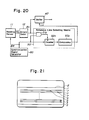
- FIG. 20 is a block diagram of the structure to show the fourth embodiment of this invention
- FIG. 21 is a plane view to show another embodiment of the optical recording medium form which data is read out in accordance with this invention.
- FIGs. 1 and 3 show the structure of the first embodiment of the optically recorded data reading device.
- the device for reading optically recorded data shown in the figures is the second embodiment of this invention as well as a device with which the method for reading optically recorded data according to the first invention is conducted.
- the device for reading out optically recorded data illustrated in the figures is a device which reads out data from an optical recording medium provided with data recording regions defined by reference lines in stripe and with a large number of data tracks perpendicular to said data recording regions.
- the device comprises a reading means 10, a gate circuit 20, a reference line detecting means 50, a reading position modification indicating means 60, a reading position indicating means 70, and a synchronizing signal generator 80, and further includes a decoder 30 which decodes read out signals, and a buffer 40 which holds decoded signals.
- the reading means 10 comprises a reading sensor 11 having a sensing field covering plural data tracks including the particular data track which should be read and reference lines defining the tracks which reads data from an end of the field and outputs video signals thereof, and a binary coder 12 which codes the video signals from the sensor 11 into binary signals Bs and outputs the same.
- the reading sensor 11 may be a CCD linear sensor and as shown in FIG. 2, is provided with photodetectors forming a field F which is longer than ca. four recording regions of an optical recording medium.
- the photodetectors are provided in the number ca. four times the number of memory cells in one track, for instance, 2048 elements in this embodiment, and arranged at an interval corresponding to that of the cells.
- the reading sensor 11 reads data by accu- mutating electric charges in proportion to the amount of light received by each photodetector, and serially outputting the charges in accordance with synchronizing signals 0R which will be described hereinafter. The output thereof becomes video signals Vd for each track.
- the binary coder 12 may be a comparator which compares said video signals Vd with a reference value and codes the same into binary signals Bs.
- the gate circuit 20 may be an AND gate which controls transmission of the output signals of said reading means 10.
- Said reference line detecting means 50 comprises a signal level discriminator 51 which takes out signals of a predetermined output level corresponding to the reference line from the binary signals Bs, a time duration counter 52 which counts the duration of the taken out signal, and a decision circuit 53 which monitors whether or not said duration exceeds a predetermined value and if so, outputs reference line detection signals Ls.
- FIG. 4 shows an embodiment of the structure of the reference line detecting means 50.
- the signal level discriminator 51 may be an AND gate 51 a which receives as inputs said synchronizing signals 0R and inverted binary signals Bs.
- the time duration counter 52 may be a counter 52a which counts synchronizing signals 0R.
- the counter 52a is reset with high level signals from the AND gate 51a.
- the decision circuit 53 may be a comparator 53a which compares the counted value from the counter 52a with a predetermined reference value and if the counted value exceeds the reference value, outputs reference line detection signals Ls.
- the reading position modification indicating means 60 comprises a target reference line detection circuit 61 which detects the first reference line which comes in the field out of said reference line detection signals Ls, a reading position detecting circuit 62 which detects the position of the data which is being scanned with said reading sensor 11 within the field, and a shift indicator 63 which compares the position of the first reference line detected by the target reference detection circuit 61 with the reading position at the preceding scanning, monitors whether or not there is any drastic change between said two, and if there is a drastic change, outputs a shift command Ss which directs a shift of the reading position in accordance with the direction of such a change.
- FIG. 5 shows the structure of the reading position modification indicator 60.
- the target reference line detector comprises a flip-flop 61 a and an AND gate 61b.
- the flip-flop 61 a inputs synchronizing signal 0T at a set terminal S for giving a starting timing for each scanning, inputs the reference line detection signals Ls at a reset terminal R, and connects the Q output therefrom with the input of the AND gate 61 b.
- the AND gate 61 b receives as input the reference line detection signals Ls.
- the reading position detector 62 may be a counter 62a which is reset with synchronizing signals 0T and counts synchronizing signals 0R.
- the shift indicator 63 may comprise a current value memory 63a, a preceding value memory 63b and an arithmetic circuit 63c.
- the memories may be registers.
- the outputs from the AND gate 61 b are inputted at the enabling terminals E of the current value memory 63a and of the arithmetic circuit 63c and when said outputs are at high level, data are taken in.
- the current value memory 63a and the preceding value memory 63b are so constructed that the contents of the memory 63a will be transferred to the memory 63b by means of synchronizing signals 0T.
- the arithmetic circuit 63c has an arithmetic function as well as a decision function and is connected at the input thereof with the counter 62a and the preceding value memory 63b. The arithmetic circuit 63c obtains the difference therebetween and if the difference becomes re- markabfy large, outputs either + 1 or -1 as a shift command Ss in correspondence with the sign of the difference.
- the reading position indicating means 70 comprises a reference line counter 71 which counts the signals Ls in order to detect the reference lines defining the particular data recording region to be read out, and a reading position decision circuit 72 which decides the position of the data recording region which should be read out on the basis of the counted values from the reference line counter 71 and the shift command Ss.
- FIG. 6 shows an example of the structure of the reading position decision circuit 72.
- the reference line counter 71 may be a counter 71a a which counts the reference line detection signals Ls.
- the reading position decision circuit 72 comprises a comparator 72a which compares the counted value from the counter 71 a with a target value to determine the position of the data recording region which should be read and outputs gate signals Gs, and an up-down counter 72b which has a function for presetting the target value as well as an up-down function to modify said target value with shift commands Ss.
- the synchronizing signal generator 80 outputs synchronizing signals 0R as a reset pulse for transferring the electric charges accumulated in photodetectors and synchronizing signals ⁇ T which synchronizes start of transfer for each track to the reading sensor, and outputs synchronizing signals to a driving controller (not shown) for the start of relative movement between the reading sensor and the recording medium.
- the synchronizing signal 0R in this embodiment is outputted in the number of pulses corresponding to the number of elements of the reading sensor 11 between the two synchronizing signals 0T and 0T.
- data should be coded by FM encoding.
- FIM encoding "1 " which is a digital data of one bit is represented by two bits of "0, 1 " or “1, 0” while "0” is represented by “0, 0” or “1, 1”. If the reference line 7 is formed to continue a low level - (or high level) for a certain period of time, it can be easily discriminated from data.
- a reading sensor 11 is carried by a moving controller (not shown) to oppose to the track on the recording region which should be read.
- the synchronizing signal generator 80 issues synchronizing signals 0T as shown in FIG. 7a to start the reading operation of the sensor 11.
- the reading sensor 11 transfers in serial the electric charges accumulated in each photodetector and outputs video signals Vd as shown in FIG. 7c. These video signals Vd are sent to a binary coder 12 to be encoded into binary signals.
- the reading sensor When the reading sensor has completed reading one track data, it is moved by the moving controller to the next track to read the data therefrom by repeating the same operation.
- the reading sensor 11 moves along the data recording region on the medium C to read data track by track.
- the scope of the sensing field which the sensor can hold simultaneously is limited to several regions, and may be as wide as four regions in this embodiment as shown in FIGs. 8A and 8B.
- the standard position herein is the position which covers four reference lines 7 within the field F.
- the binary signals Bs are sent to the gate 20 and the reference line detecting means 50. Only when the gate is open, the signal Bs can be sent to the decoder 30.
- the synchronizing signals OR are counted by the counter 52a and the counted value is sent to the comparator 53a.
- the binary signals Bs are sampled using the synchronizing signal 0R as a gate signal. When both synchronizing signal ⁇ R and the binary signal Bs are at high level, the output from the AND gate 51 a becomes high level. Consequently, the counter 52a is reset.
- the counter 52a has been counting the synchronizing signals ⁇ R and everytime it is reset, it starts counting anew. Therefore, when the output in binary signals Bs keeps low level for a long time, the yalues counted by the counter 52a are accumulated, but as the counter is otherwise reset at a short interval, the counted values would not be accumulated for a long time.
- the comparator 53a compares the counted values by the counter 52a with a preset time length. When the counted value reaches the preset value, the comparator 53a outputs reference line detection signals Ls.
- the reference line detection signals Ls are sent to the reading position modification indicating means 60 and the reading position indicating means 70.
- the signals are inputted at the flip-flop 61 a which acts as the target reference line detecting means and the AND gate 61 b.
- the flip-flop 61 a is reset with the synchronizing signal 0T to make the output terminal Q high level and is reset with the reference line detection signals Ls to make the output terminal Q low level.
- the synchronizing signal 0T is outputted at the start of each scanning, and the flip-flop 61a a is therefore set at every scanning. It is reset with the input of the reference line detection signals Lc.
- the output of AND gate 61 becomes higher in level only when the above output terminal Q becomes high level and the above reference line detection signals Ls are inputted. This means that the output of the target reference line detector 61 becomes high level only when the reference line coming into the field is inputted.
- This output is an enabling signal to the current value memory 63a and the arithmetic circuit 63c which will be described hereinafter. When these outputs become high level, the current value memory 63a and the arithmetic circuit 63c are enabled to take in data.
- the counter 62a has been counting synchronizing signals 0R.
- the counter is reset everytime synchronizing signal 0T is inputted to start counting anew.
- the counted values are taken in by the current value memory 64a and the arithmetic circuit 63c of the shift indicator 63.
- the value counted by the current value memory 64a is transferred to the preceding value memory 63b in synchronization with synchronizing signals 0T.
- the counted values stored at the preceding value memory 63b are taken in by the arithmetic circuit 63c with enabling signals from the AND gate 61 b.
- the arithmetic circuit 63c compares said counted value from the counter 62a with the counted values stored in the preceding value memory 63b, and if there is a drastic change in the difference, outputs signals of either + 1 or -1 depending on the sign of the difference as shift command signals Ss. It does not issue any signals if there is no such drastic change in the difference.
- the counter 71 a counts the reference line detection signals Ls and the comparator 72a compares the counted values with the target value to detect the data recording region which should be read out.
- the target value is present by the preset function of the up-down counter 72b.
- the up-down counter 72b is preset with [2]. If it is desired to read out the data recording region sandwiched between the third and the fourth lines from the top of the field as shown in FIG. 8B by F 3, on the other hand, the up-down counter 72b is preset with [3].
- the reading sensor 11 outputs video signals Vd as shown in FIG. 9A by Vd 1.
- the reference line detection signal Ls as shown by Ls 1 in FIG. 9A is outputted as the first signal of the current field.
- the counter 71 a counts the reference line detection signals Ls and if the counted values reaches the target [2] preset at the up-down counter 72b, the comparator 72a starts outputting the gate signals.
- the gate 20 On receiving the gate signals, the gate 20 opens. Consequently, the binary code signals Bs outputted from the reading means 10 are sent to the decoder 30 to be decoded and the decoded contents thereof are stored at the buffer 40.
- the reading sensor 11 is moved in relation to the longitudinal direction of the data recording regions to read the data from adjacent data track. In this manner, the sensor 11 can read out data sequentially from adjacent tracks.
- the reading sensor 11 should be precisely opposed in parallel to data tracks, perfect parallel relation is difficult to maintain in practice. They often oppose to each other at a slight angle on two parallel planes. Such an angular deviation may displace the sensing field of the reading sensor 11 toward the direction of data tracks as it is moved relatively in the longitudinal direction thereof even though such deviation may be quite negligible for data reading.
- the data recording region is also deviated.
- the displacement is monitored by the reading position modification indicating means 60 according to this invention.
- the reading position modification indicating means 60 detects the reference lines which are the target of the monitoring (in this embodiment the reference line coming first in the field F) from the signals Ls by means of the target reference line detector 61 comprising the flip-flop 61a and the AND gate 62b. Simultaneously the counter 62a is reset with synchronizing signal 0T to count synchronizing signals OR for each scanning.
- the target reference line detector 61 detects the reference line, the counted values are inputted at the current value memory 63a and the arithmetic circuit 63b of the shift indicator 63. The values thus stored at the memory are transferred to the preceding value memory 63b in synchronization with the next synchronizing signal 0T.
- the arithmetic circuit 63c is enabled with enabling signals which are issued when the target reference line detector 61 detects the target reference line, compares the counted values at the preceding scanning from the preceding value memory 63b with the counted values at the current scanning from the current value memory 62a to obtain the difference therebetween. If the difference is small, it does not output any signals when the difference is remarkably large, it outputs a shift command with a sign corresponding to that of the difference.
- the detection position of the reference line detection signal Ls becomes as shown by Ls 1 in FIG. 9A at the preceding scanning and like the one shown by Ls 2 in FIG. 9A at the current scanning, indicating a remarkable change.
- This drastic change is caused by the fact that as shown in FIG. 8A, the field F of the reading sensor 11 is deviated upward as the field F2 and the reference line which was not included in the field F1 at the preceding scanning newly appears at the starting end of the field F2. Therefore, the arithmetic circuit 63c outputs a shift command Ss to count up the target value by + 1.
- the detection position of the reference line detection signal Ls becomes like the one shown by Ls 3 at the preceding scanning and like the one shown by Ls 4 in FIG. 9B at the current scanning, indicating a drastic change.
- the arithmetic circuit 63c outputs a shift command of -1 to count down the target value.
- the counter 71 a counts the reference line detection signals Ls and sends the counted values to the comparator 72b.
- the up-down counter 72b increases/decreases by one the preset target value with a shift command Ss. For instance, if the preset target value is [2] and if the sensor is deviated as shown in FIG. 8A by F2, the target value is modified into [3] and when the counter 71 a has counted 3 reference lines, the comparator 72a outputs a gate signal Gs. When the preset target value is [3] and the sensor is deviated as shown in FIG. 8B by F4, the target value is modified into [2] and when the counter 71 has counted 2 reference lines, the comparator 72a outputs a gate signal Gs.
- the gate 20 is opened to allow the binary code signals Bs form the reading means 10 to be inputted at the decoder 30.
- the next reference line is detected, the number of reference lines counted exceeds the target value, so that the comparator 72a stops outputting the gate signals. This makes the decoder 30 to receive selectively the track data of the targetted recording regions.
- This invention also enables data to be read out precisely from the aimed data track even if the reading sensor is relatively moved in the longitudinal direction of data recording regions with its sensing field inclined at an angle against the regions such that the field F is deviated vertically from the regions.
- FIG. 13 shows the structure of the second embodiment of the optically recorded data reading device.
- the device for reading optically recorded data shown in the figure comprises a reading means 10 which includes a reading sensor and a binary coder, a reference line detecting means 50 which includes a signal level discriminator 51, a time duration counter 52 and a decision circuit 53, a reading position indicating means 70 which includes a reference line counter 71 and a reading position decision circuit 72, and a synchronizing signal generator 80, and is further provided with a decoder 30 for decoding read out signals and a buffer 40 for holding the decoded signals.
- This embodiment is substantially the same as the first embodiment in structure except that the gate circuit 20 and the reading position modification indicating means 60 are not included in the second embodiment and that the reading position indicating means 70 and the decoder 30 respectively differ structurewise from the first embodiment.
- the second embodiment will now be described focusing mainly on these differences.
- the decoder 30 having a gate function at input is used.
- the reading position indicating means 70 is correspondingly simplified in structure.
- the reading position indicating means 70 is provided with a counter 71 a as the reference line counter 71 which counts reference lines out of reference line detection signals Ls so as to detect the reference lines defining a particular data reading region.
- a comparator 72a is also provided to act as the reading position decision circuit 72 to decide the position of the data recording region by comparing the counted values from the counter 71 with the preset target value.
- the counter 71 a and the comparator 72a are identical to those used in the first embodiment, but the up-down counter for setting the target value is not provided.
- the target value is determined by the sequential order of the reference lines which define the data recording regions appearing in the field. Unlike the first embodiment, the target value in this embodiment is fixed and is therefore preset at the comparator 72a.
- the target value may be variable. In that case, a digital switch, register and the like may be used as the target value setting means.
- the operation of the second embodiment having the above structure will now be described referring to the figures mentioned.
- the operation is essentially the same as that of the first embodiment except for the modification of the reading position which is not included in this embodiment.
- the reading position decision circuit 72 will therefore be described in detail as the operational differences lie there.
- the data read by the reading means 10 are encoded into binary signals Bs and sent to the decoder 30 and the reference line detecting circuit 50.
- the binary signal Bs can be inputted at the decoder 30 only when an input enabling signal is transmitted from the reading position decision circuit 72.
- the reference lines are detected from the binary signals Bs and outputted as the reference line detection signals Ls.
- the reference line detection signals Ls are counted by the counter 71 a, and the counted value is sent to the comparator 72a.
- the comparator 72a compares the counted value with the target value, and when the counted value remains identical with the target value, outputs input enabling signals (the signal may be a gate signal Gs as in the first embodiment) to the decoder 30.
- the target data are selectively inputted at the decoder 30 in this manner.
- FIG. 15 shows a schematic view of the structure of the third embodiment according to the present invention.
- the optically recorded data reading device to which the third embodiment will be applied comprises a reading means which includes a reading sensor 11 to read out data by following the data tracks in the data recording regions in the optical data recording medium (not shown), a buffer 41 which holds the read out data, a movement controller 90 which controls the relative movements of the reading sensor 11 and the optical data recording medium to cause the sensor 11 to follow the data tracks in the data recording regions, and a synchronizing signal generator 80 which sends synchronizing signals to the sensor 11 and to the movement controller 90 for controlling.
- a reading means which includes a reading sensor 11 to read out data by following the data tracks in the data recording regions in the optical data recording medium (not shown), a buffer 41 which holds the read out data, a movement controller 90 which controls the relative movements of the reading sensor 11 and the optical data recording medium to cause the sensor 11 to follow the data tracks in the data recording regions, and a synchronizing signal generator 80 which sends synchronizing signals to the sensor 11 and to the movement controller 90 for controlling.
- the reading sensor 11 is provided with photodetectors in the number two times the number of memory cells in one track, for instance 1024 elements in this embodiment, and arranged at an interval corresponding to that of the cells.
- the structure and the operation are essentially the same as those in the first embodiment.
- the reading means 10 is provided with a binary coder 12 which encodes said video signals Vd into binary signals Bs.
- the binary signals Bs are stored at the buffer 41.
- the movement controller 90 comprises a driving control circuit 91 which forms driving signals on the basis of synchronizing signals sent from the synchronizing signals generator 80, and a moving device 92 which relatively moves the reading sensor 11 and the optical recording medium in accordance with the driving signals.
- the synchronizing signal generator 80 supplies the reading sensor 11 with synchronizing signals 0R as shift pulses for transferring electric charges accumulated at the photodetecors and synchronizing signals 0T for synchronizing the start of transfer in each track. It also outputs synchronizing signals to start moving the driving control circuit.
- the synchronizing signals ⁇ R in this embodiment are outputted between the two synchronizing signals 0T, 0T in 1024 pulses which correspond to the number of elements in the reading sensor 10.
- the data reading device is further provided with a reference line detecting means 50 which detects the reference lines from binary .signals Bs outputted from the binary coder 12 and a tracking decision means 100 which decides whether the position of the reference lines detected by the reference line detecting means 50 is within the predetermined tolerance.
- the reference line detecting means 50 comprises a signal level discriminator 51 which takes out signals of a predetermined output level corresponding to the reference lines from the binary signals Bs of the binary coder 12, a time duration counter 52 which counts the duration of the signals taken out at the circuit 51 and when the duration reaches the time corresponding to the width of the reference lines, outputs reference line detection signals, and a decision circuit 53.
- the reference line detecting means 50 differs in structure from that of the first embodiment. The same structure may of course be applicable.
- the signal level discriminator 51 may be an AND gate 54 as shown in FIG. 16, and receives said synchronizing signals 0R and the inverted binary signals Bs.
- the time duration counter 52 and the decision circuit 53 may be a preset counter 55, for example, as shown in FIG. 16.
- the preset counter 55 counts the outputs from the AND gate 54 when they are in high level, and when the counted value reaches a preset value, outputs reference line detection signal pulses.
- the preset value is given as the number of synchronizing signals 0R corresponding to the time length necessary for the reading sensor 11 to read out the width of the reference lines.
- the value corresponds to 40 pulses in this embodiment and is substantially fixed. Although the counted value is reset by the synchronizing signal 0T every time the track changes, the preset value is not reset.
- the tracking decision means 100 comprises a reading position detecting means 101 which detects the current reading position in correspondence with the serial scanning of the sensor 11 track by track, a tolerance setting means 102 which predetermines a tolerance as a reference value in which scope the presence of reference lines are permitted, and a comparator 103 which compares whether or not the reading position at the time when the reference line detection signal is outputted is within the tolerance.
- the reading position detecting means 101 may be a counter 104 which is reset by the synchronizing signal 0T each time the track changes, and counts the synchronizing signals 0R synchronously with the transfer of the read data from each track.
- the tolerance setting means 102 may be a memory 105 as shown in FIG. 16 which sets the reference value for indicating the tolerance in the number of memory cells from the starting end of the tracks.
- the reference value is such that the optical system including the reading sensor is placed at a standard position which enables the first reference line to terminate at the 256th 0R from the first 0T.
- the tolerance is set at a value of ⁇ 8 of the counted 0R.
- the comparator 103 comprises an arithmetic circuit 106 as shown in FIG. 16.
- the arithmetic circuit 106 is actuated with the output pulse from the preset counter 55, reads in the reference value data from the memory 105 as well as the current value from the counter 104 and compares the two. If the counted value is within the tolerance, the arithmetic circuit 106 outputs a normal status signal; Otherwise, a status signal indicating to that effect as well as a signal indicating the extent of a deviation are outputted to the movement controller 91.
- the movement controller causes the reading sensor 11 to oppose to tracks of the data recording region which should be read out.
- the synchronizing signals 0T as shown in FIG. 17 are sent from the synchronizing signal generator 80 to start the reading sensor 11.
- the reading sensor 11 serially transfers electric charges accumulated at the photodetectors with the synchronizing signals ⁇ R (see FIG. 17b) and outputs video signals Vd as shown in FIG. 17c.
- the video signals are sent to the binary coder 12 to become binary signals.
- the reading sensor 11 Having completed reading one data track in this manner, the reading sensor 11 is moved to the next track by the movement controller and starts scanning anew.
- the reading sensor 11 In order to read the data accurately, the reading sensor 11 must be opposed in parallel to the data trains to be read, i.e. tracks. This means that the reading sensor must precisely follow the data trains.
- the third embodiment solves the problem in this respect.
- the reading sensor 11 moves along the data recording regions 3 on the optical recording medium 1, reading the data track by track.
- the sensing field F of the reading sensor 11 at one time is the width equivalent to ca. 2 data recording regions, as shown in FIG. 18.
- the standard operation requires that two reference lines 7 must always be included in the field F. Therefore, like the first embodiment, video signals Vd are outputted from the reading sensor 11 synchronously with the signals 0T, 0R.
- the video signals are sent to the binary coder 12 as described above to become binary signals. They are stored at the buffer 41 and at the same time sent to the reference line detecting means 50.
- the binary signals Bs are inverted and inputted at the AND gate 54 which constitutes the signal level discriminator 51.
- the synchronizing signals 0R are also inputted at the AND gate 54.
- the AND gate 54 outputs pulses which synchronize with the signals 0R when the binary signal Bs is at a low level. It is noted that for easier signal discrimination, data are FM encoded in advance as in the first embodiment.
- These pulses are counted by the preset counter 55.
- the preset counter 55 is set with a predetermined value in advance. When the counted value reaches the predetermined value, the counter outputs pulses. The counted values are reset when a synchronizing signals 0T is inputted.
- the counter 104 counts the synchronizing signals 0R. The counting is reset each time a synchronizing signal 0T is inputted to start counting operation anew.
- the pulses outputted from the preset counter 55 are inputted at the arithmetic circuit 106.
- the arithmetic circuit 106 Upon receiving the pulses, the arithmetic circuit 106 reads out the reference value (256 ⁇ 8 in this embodiment) which has been previously inputted and which corresponds to the position of the reference line. At the same time, the circuit 106 reads in the counted values of the counter 104. The circuit 106 compares the reference value with the counted values for their difference and when the value is within the tolerance of the reference lines indicated by the reference value, outputs a status signal indicating to that effect. On the other hand, as shown in FIG. 19, if the values fall out of the tolerance, a status signal inidicating a tracking error is outputted.
- the status data are inputted at the buffer 41 and the driving control circuit 91 in this embodiment.
- the status signal inputted at the buffer 41 is used as a signal to decide whether or not the currently read out data is normal.
- the moving device 92 moves the reading sensor 11 on the basis of the status data as well as the result obtained from the arithmetic circuit 106 to modify the position by moving the reading sensor 11 by the moving device 92.
- the output signal of the decision circuit 100 is utilized to automatically modify the position of the reading sensor 11, it is also possible that a normal or abnormal status signals may be outputted.
- the optically recorded data reading device shown in the figure comprises as essential components a reading sensor 11 which reads the data following the tracks 4 on a data recording region 3 as shown in FIG. 12, a binary coder 12 which encodes the output video signals from the sensor 11 into binary signals, a buffer 42 which temporarily stores the binary signals Bs, a reference line detecting means 50 which detects the reference lines 7 from the binary signals Bs, and a synchronizing signal generator 80.
- the components of the fourth embodiment except for the buffer 42 are identical in structure and operation to those of the first and third embodiments. Therefore, only the different aspects will be explained.
- the buffer 42 comprises input/output control gates and a register. It altemately opens/closes the control gates at the input and the output in accordance with the input of the reference line detection signal Ls (which will be described later), stores the binary signals Bs and outputs the previously stored binary signals Bs.
- the signals Ls are sent to the buffer 42.
- the buffer 42 opens the input gate with the first reference line detection signal Ls while closing the output gate therewith.
- the buffer 42 closes the input gate and opens the output gate.
- the output from the reading sensor 10 which covers these two reference lines, the data of the track defined by these two lines, and data of a portion of the tracks outside these two lines are read to extract the data of the particular track which should be read.
- the field F of the sensor 11 is somewhat deviated vertically (in the direction of tracks), data can be accurately read out without minute and complicated positional correction.
- the present invention is not limited to the above embodiments but can be modified in structure.
- the reading position indicating means of the first embodiment changes the target value to correct the deviation of the field
- a gate circuit is provided separately in the first embodiment, the gate may be incorporated in the decoder, the reading position indicating means or the like.
- the length of the sensing field is determined to cover the length of four data recording regions, but it may cover five regions or more.
- the first reference line appearing in the field is the target of monitoring.
- the target reference line may be the second or thereafter.
- the present invention is further applicable to optical recording medium such as shown in FIG. 21.
Applications Claiming Priority (6)
| Application Number | Priority Date | Filing Date | Title |
|---|---|---|---|
| JP8348285A JPS61242339A (ja) | 1985-04-18 | 1985-04-18 | 光記録媒体の基準線検知装置 |
| JP83482/85 | 1985-04-18 | ||
| JP8569785A JPS61243944A (ja) | 1985-04-22 | 1985-04-22 | 光記録情報読取装置のデ−タ列検知装置 |
| JP85697/85 | 1985-04-22 | ||
| JP106640/85 | 1985-05-18 | ||
| JP10664085A JPS61264517A (ja) | 1985-05-18 | 1985-05-18 | 光記録情報読取方法および装置 |
Publications (2)
| Publication Number | Publication Date |
|---|---|
| EP0200434A1 true EP0200434A1 (fr) | 1986-11-05 |
| EP0200434B1 EP0200434B1 (fr) | 1990-11-07 |
Family
ID=27304236
Family Applications (1)
| Application Number | Title | Priority Date | Filing Date |
|---|---|---|---|
| EP86302929A Expired - Lifetime EP0200434B1 (fr) | 1985-04-18 | 1986-04-18 | Procédé de lecture de données enregistrées optiquement et dispositif à cet effet |
Country Status (3)
| Country | Link |
|---|---|
| US (1) | US4855981A (fr) |
| EP (1) | EP0200434B1 (fr) |
| DE (1) | DE3675426D1 (fr) |
Cited By (9)
| Publication number | Priority date | Publication date | Assignee | Title |
|---|---|---|---|---|
| EP0224250A2 (fr) * | 1985-11-26 | 1987-06-03 | Csk Corporation | Support d'enregistrement optique et méthode et appareil pour en corriger la déviation angulaire |
| EP0224251A2 (fr) * | 1985-11-26 | 1987-06-03 | Computer Services Corporation | Méthode et appareil pour corriger la déviation angulaire d'un support d'enregistrement optique |
| EP0231009A2 (fr) * | 1986-01-27 | 1987-08-05 | Csk Corporation | Milieu d'enregistrement optique |
| EP0279696A2 (fr) * | 1987-02-20 | 1988-08-24 | Canon Kabushiki Kaisha | Méthode d'accès d'une piste dans un milieu d'enregistrement à l'arrêt et appareil correspondant |
| EP0296590A2 (fr) * | 1987-06-23 | 1988-12-28 | Omron Tateisi Electronics Co. | Appareil de traitement de carte optique |
| EP0300481A2 (fr) * | 1987-07-22 | 1989-01-25 | Omron Tateisi Electronics Co. | Appareil pour détecter l'inclinaison d'une carte optique |
| EP0301537A2 (fr) * | 1987-07-31 | 1989-02-01 | Olympus Optical Co., Ltd. | Appareil d'enregistrement/reproduction à carte optique |
| US5179268A (en) * | 1987-07-22 | 1993-01-12 | Omron Tateisi Electronic Co. | Apparatus for detecting inclination of an optical card |
| US5264687A (en) * | 1987-06-23 | 1993-11-23 | Omron Tateisi Electronics, Co. | Optical card processing apparatus |
Families Citing this family (8)
| Publication number | Priority date | Publication date | Assignee | Title |
|---|---|---|---|---|
| US5280160A (en) * | 1987-02-27 | 1994-01-18 | Canon Kabushiki Kaisha | Recording and reproducing method and apparatus compensating for predicted deviation based on detected relative skewing of recording medium |
| US5187698A (en) * | 1988-09-20 | 1993-02-16 | Kabushiki Kaisha Csk | Data reading apparatus for identifying position of data tracks |
| JPH07117978B2 (ja) * | 1988-09-20 | 1995-12-18 | 株式会社シーエスケイ | 光記録媒体の読取りシステム |
| US5138140A (en) * | 1990-08-22 | 1992-08-11 | Symbol Technologies, Inc. | Signature capture using electro-optical scanning |
| JPH04356729A (ja) * | 1991-03-28 | 1992-12-10 | Olympus Optical Co Ltd | 光学的情報記録再生装置 |
| JPH04335214A (ja) * | 1991-05-09 | 1992-11-24 | Olympus Optical Co Ltd | 情報記録再生装置 |
| US5199084A (en) * | 1991-08-16 | 1993-03-30 | International Business Machines Corporation | Apparatus and method for locating characters on a label |
| US7436760B2 (en) * | 2003-08-21 | 2008-10-14 | Transpacific Ip, Llp | Method for reading sensor |
Citations (6)
| Publication number | Priority date | Publication date | Assignee | Title |
|---|---|---|---|---|
| DE3039902A1 (de) * | 1979-10-23 | 1981-05-07 | Tokyo Shibaura Denki K.K., Kawasaki, Kanagawa | Verfahren zur indexinformations-aufzeichnung und bildinformations-aufzeichnungsvorrichtung |
| EP0038499A1 (fr) * | 1980-04-15 | 1981-10-28 | Matsushita Electric Industrial Co., Ltd. | Système d'enregistrement et de restitution d'information par voie optique |
| EP0054438A1 (fr) * | 1980-12-17 | 1982-06-23 | Matsushita Electric Industrial Co., Ltd. | Disque optique à signe indicateur |
| EP0122144A1 (fr) * | 1983-04-07 | 1984-10-17 | Plasmon Data Systems N.V. | Stockage optique de données |
| EP0131455A2 (fr) * | 1983-07-07 | 1985-01-16 | Freund Precision, Inc. | Carte d'identification non falsifiable et système d'identification |
| EP0164131A2 (fr) * | 1984-06-07 | 1985-12-11 | Victor Company Of Japan, Limited | Disque d'enregistrement d'informations et procédé et appareil pour enregistrer ou reproduire des informations |
Family Cites Families (10)
| Publication number | Priority date | Publication date | Assignee | Title |
|---|---|---|---|---|
| JPS5331920A (en) * | 1976-09-06 | 1978-03-25 | Nippon Denso Co Ltd | Bar code reader |
| US4189783A (en) * | 1977-02-25 | 1980-02-19 | Stanford Research Institute | Mass storage of books |
| US4536866A (en) * | 1978-11-30 | 1985-08-20 | Videonics Of Hawaii, Inc. | Information retrieval system and apparatus |
| US4283777A (en) * | 1979-05-14 | 1981-08-11 | Xerox Corporation | Optical memory having a parallel read out |
| US4321622A (en) * | 1979-11-26 | 1982-03-23 | Mcdonnell Douglas Corporation | Video track transfer system and method |
| US4357596A (en) * | 1980-05-30 | 1982-11-02 | Westinghouse Electric Corp. | Multi-line scan mark verification circuit |
| US4695991A (en) * | 1980-12-09 | 1987-09-22 | Storage Research Pty. Ltd. | Reading information stored in multiple frame format |
| US4634850A (en) * | 1983-10-12 | 1987-01-06 | Drexler Technology Corporation | Quad density optical data system |
| US4598393A (en) * | 1984-04-06 | 1986-07-01 | Drexler Technology Corporation | Three-beam optical servo tracking system with two-track parallel readout |
| US4652730A (en) * | 1985-01-03 | 1987-03-24 | Honeywell Information Systems Inc. | Method and apparatus for skew compensation in an optical reader |
-
1986
- 1986-04-17 US US06/853,339 patent/US4855981A/en not_active Expired - Fee Related
- 1986-04-18 EP EP86302929A patent/EP0200434B1/fr not_active Expired - Lifetime
- 1986-04-18 DE DE8686302929T patent/DE3675426D1/de not_active Expired - Fee Related
Patent Citations (6)
| Publication number | Priority date | Publication date | Assignee | Title |
|---|---|---|---|---|
| DE3039902A1 (de) * | 1979-10-23 | 1981-05-07 | Tokyo Shibaura Denki K.K., Kawasaki, Kanagawa | Verfahren zur indexinformations-aufzeichnung und bildinformations-aufzeichnungsvorrichtung |
| EP0038499A1 (fr) * | 1980-04-15 | 1981-10-28 | Matsushita Electric Industrial Co., Ltd. | Système d'enregistrement et de restitution d'information par voie optique |
| EP0054438A1 (fr) * | 1980-12-17 | 1982-06-23 | Matsushita Electric Industrial Co., Ltd. | Disque optique à signe indicateur |
| EP0122144A1 (fr) * | 1983-04-07 | 1984-10-17 | Plasmon Data Systems N.V. | Stockage optique de données |
| EP0131455A2 (fr) * | 1983-07-07 | 1985-01-16 | Freund Precision, Inc. | Carte d'identification non falsifiable et système d'identification |
| EP0164131A2 (fr) * | 1984-06-07 | 1985-12-11 | Victor Company Of Japan, Limited | Disque d'enregistrement d'informations et procédé et appareil pour enregistrer ou reproduire des informations |
Cited By (19)
| Publication number | Priority date | Publication date | Assignee | Title |
|---|---|---|---|---|
| US4881215A (en) * | 1985-11-26 | 1989-11-14 | Computer Services Corporation | Optical recording medium and method for correcting angular deviation thereof |
| EP0224250A2 (fr) * | 1985-11-26 | 1987-06-03 | Csk Corporation | Support d'enregistrement optique et méthode et appareil pour en corriger la déviation angulaire |
| EP0224251A3 (en) * | 1985-11-26 | 1989-07-26 | Computer Services Corporation | Method and apparatus for correcting angular deviation of optical recording medium |
| EP0224250A3 (en) * | 1985-11-26 | 1989-07-26 | Computer Services Corporation | Optical recording medium and method and apparatus for correcting angular deviation thereof |
| EP0224251A2 (fr) * | 1985-11-26 | 1987-06-03 | Computer Services Corporation | Méthode et appareil pour corriger la déviation angulaire d'un support d'enregistrement optique |
| EP0231009A3 (en) * | 1986-01-27 | 1990-01-10 | Csk Corporation | Optical recording medium |
| EP0231009A2 (fr) * | 1986-01-27 | 1987-08-05 | Csk Corporation | Milieu d'enregistrement optique |
| EP0279696A2 (fr) * | 1987-02-20 | 1988-08-24 | Canon Kabushiki Kaisha | Méthode d'accès d'une piste dans un milieu d'enregistrement à l'arrêt et appareil correspondant |
| US4982391A (en) * | 1987-02-20 | 1991-01-01 | Canon Kabushiki Kaisha | Method and apparatus for accessing a desired track of a recording medium during a stopped state of recording or reproduction |
| EP0279696A3 (en) * | 1987-02-20 | 1989-05-24 | Canon Kabushiki Kaisha | Method of accessing track in still state of recording medium and apparatus thereof |
| US5264687A (en) * | 1987-06-23 | 1993-11-23 | Omron Tateisi Electronics, Co. | Optical card processing apparatus |
| EP0296590A3 (en) * | 1987-06-23 | 1989-10-18 | Omron Tateisi Electronics Co. | Optical card processing apparatus |
| EP0296590A2 (fr) * | 1987-06-23 | 1988-12-28 | Omron Tateisi Electronics Co. | Appareil de traitement de carte optique |
| EP0300481A3 (en) * | 1987-07-22 | 1990-04-18 | Omron Tateisi Electronics Co. | Apparatus for detecting inclination of optical card |
| EP0300481A2 (fr) * | 1987-07-22 | 1989-01-25 | Omron Tateisi Electronics Co. | Appareil pour détecter l'inclinaison d'une carte optique |
| US5179268A (en) * | 1987-07-22 | 1993-01-12 | Omron Tateisi Electronic Co. | Apparatus for detecting inclination of an optical card |
| EP0301537A3 (en) * | 1987-07-31 | 1989-09-13 | Olympus Optical Co., Ltd. | Optical card recording/reproducing apparatus |
| EP0301537A2 (fr) * | 1987-07-31 | 1989-02-01 | Olympus Optical Co., Ltd. | Appareil d'enregistrement/reproduction à carte optique |
| US4950876A (en) * | 1987-07-31 | 1990-08-21 | Olympus Optical Co., Ltd. | Optical card recording/reproducing apparatus with compensation for displacement deviation between data area of optical card and laser beam |
Also Published As
| Publication number | Publication date |
|---|---|
| US4855981A (en) | 1989-08-08 |
| EP0200434B1 (fr) | 1990-11-07 |
| DE3675426D1 (de) | 1990-12-13 |
Similar Documents
| Publication | Publication Date | Title |
|---|---|---|
| EP0200434B1 (fr) | Procédé de lecture de données enregistrées optiquement et dispositif à cet effet | |
| CA1298652C (fr) | Carte d'enregistrement optique et methode de lecture de cette carte | |
| US4737869A (en) | Magnetic disk having data area and index servo area and servo system for positioning read/write head on magnetic disk | |
| EP0603968A1 (fr) | Optimisation de l'écart de la mise au point pour la lecture des données enregistrées optiquement | |
| EP0409516B1 (fr) | Appareil pour la dérivation d'un signal de synchronisation des marques pré-enrégistrées sur un support d'information | |
| EP0314879B1 (fr) | Contrôle de la position relative d'une tête magnétique et d'un support d'enregistrement | |
| US4811321A (en) | Information recording medium | |
| KR100246166B1 (ko) | 광 디스크로부터의 데이타 스트림의 재정렬 | |
| EP0224251A2 (fr) | Méthode et appareil pour corriger la déviation angulaire d'un support d'enregistrement optique | |
| US4819222A (en) | Binary encoding method for data read from optical record and device therefor | |
| EP0231380A4 (en) | Method of recording data onto an optical data recording card | |
| EP0226960A1 (fr) | Système de contrôle synchronique | |
| EP0210528A2 (fr) | Milieu d'enregistrement optique et procédé d'enregistrement de données | |
| EP0295759A2 (fr) | Appareil utilisant la démodulation différentielle de données pour la protection d'écriture d'un enregistreur optique | |
| JPH0566655B2 (fr) | ||
| US5144610A (en) | Method of recording data on optical card by performing blank checking without scanning an entire track | |
| EP0630018A2 (fr) | Détection d'espaces interbloc dans un système d'enregistrement de données | |
| JPH0473217B2 (fr) | ||
| WO1983001531A1 (fr) | Procede et dispositif de positionnement d'un transducteur utilisant un codage de servo-piste noyee et une commande par microprocesseur | |
| JPS6226058B2 (fr) | ||
| JPS61246931A (ja) | 光デジタルデ−タの記録方法 | |
| JPH0555931B2 (fr) | ||
| EP0767453B1 (fr) | Synchronisation chronogramme de signaux ATF | |
| JPS6037637Y2 (ja) | 信号処理回路 | |
| JPH053660B2 (fr) |
Legal Events
| Date | Code | Title | Description |
|---|---|---|---|
| PUAI | Public reference made under article 153(3) epc to a published international application that has entered the european phase |
Free format text: ORIGINAL CODE: 0009012 |
|
| AK | Designated contracting states |
Kind code of ref document: A1 Designated state(s): DE FR GB |
|
| PUAB | Information related to the publication of an a document modified or deleted |
Free format text: ORIGINAL CODE: 0009199EPPU |
|
| PUAF | Information related to the publication of a search report (a3 document) modified or deleted |
Free format text: ORIGINAL CODE: 0009199SEPU |
|
| R17D | Deferred search report published (corrected) |
Effective date: 19861210 |
|
| RA1 | Application published (corrected) |
Date of ref document: 19861210 Kind code of ref document: A1 |
|
| 17P | Request for examination filed |
Effective date: 19870610 |
|
| 17Q | First examination report despatched |
Effective date: 19890419 |
|
| GRAA | (expected) grant |
Free format text: ORIGINAL CODE: 0009210 |
|
| AK | Designated contracting states |
Kind code of ref document: B1 Designated state(s): DE FR GB |
|
| RAP2 | Party data changed (patent owner data changed or rights of a patent transferred) |
Owner name: CSK CORPORATION |
|
| REF | Corresponds to: |
Ref document number: 3675426 Country of ref document: DE Date of ref document: 19901213 |
|
| ET | Fr: translation filed | ||
| PLBE | No opposition filed within time limit |
Free format text: ORIGINAL CODE: 0009261 |
|
| STAA | Information on the status of an ep patent application or granted ep patent |
Free format text: STATUS: NO OPPOSITION FILED WITHIN TIME LIMIT |
|
| 26N | No opposition filed | ||
| PGFP | Annual fee paid to national office [announced via postgrant information from national office to epo] |
Ref country code: GB Payment date: 19990414 Year of fee payment: 14 |
|
| PGFP | Annual fee paid to national office [announced via postgrant information from national office to epo] |
Ref country code: DE Payment date: 19990417 Year of fee payment: 14 |
|
| PGFP | Annual fee paid to national office [announced via postgrant information from national office to epo] |
Ref country code: FR Payment date: 19990427 Year of fee payment: 14 |
|
| PG25 | Lapsed in a contracting state [announced via postgrant information from national office to epo] |
Ref country code: GB Free format text: LAPSE BECAUSE OF NON-PAYMENT OF DUE FEES Effective date: 20000418 |
|
| GBPC | Gb: european patent ceased through non-payment of renewal fee |
Effective date: 20000418 |
|
| PG25 | Lapsed in a contracting state [announced via postgrant information from national office to epo] |
Ref country code: FR Free format text: LAPSE BECAUSE OF NON-PAYMENT OF DUE FEES Effective date: 20001229 |
|
| PG25 | Lapsed in a contracting state [announced via postgrant information from national office to epo] |
Ref country code: DE Free format text: LAPSE BECAUSE OF NON-PAYMENT OF DUE FEES Effective date: 20010201 |
|
| REG | Reference to a national code |
Ref country code: FR Ref legal event code: ST |