EP0200173A2 - Magnetischer Blasenspeichermodul - Google Patents
Magnetischer Blasenspeichermodul Download PDFInfo
- Publication number
- EP0200173A2 EP0200173A2 EP86105732A EP86105732A EP0200173A2 EP 0200173 A2 EP0200173 A2 EP 0200173A2 EP 86105732 A EP86105732 A EP 86105732A EP 86105732 A EP86105732 A EP 86105732A EP 0200173 A2 EP0200173 A2 EP 0200173A2
- Authority
- EP
- European Patent Office
- Prior art keywords
- case
- magnetic
- chip
- revolving
- magnetic field
- Prior art date
- Legal status (The legal status is an assumption and is not a legal conclusion. Google has not performed a legal analysis and makes no representation as to the accuracy of the status listed.)
- Granted
Links
Images


Classifications
-
- G—PHYSICS
- G11—INFORMATION STORAGE
- G11C—STATIC STORES
- G11C19/00—Digital stores in which the information is moved stepwise, e.g. shift registers
- G11C19/02—Digital stores in which the information is moved stepwise, e.g. shift registers using magnetic elements
- G11C19/08—Digital stores in which the information is moved stepwise, e.g. shift registers using magnetic elements using thin films in plane structure
- G11C19/085—Generating magnetic fields therefor, e.g. uniform magnetic field for magnetic domain stabilisation
Definitions
- This application relates to:
- the present invention relates to a magnetic bubble memory module and particularly to a magnetic bubble memory module which is suitable for thinning and miniaturizing its body lowering consumption and ameliorating efficiency of composition.
- the magnetic bubble memory module realized in these years has the structure wherein an x-coil and a Y-coil for generating a revolving magnetic field which are respectively composed of square solenoid coils having non-symmetric structures with each other are respectively inserted to E-like substrates made of ceramic, synthetic resin or the like mounting a magnetic bubble memory chip and are arranged at a right angle with eadh other.
- the X-coil and the Y-coil must be provided around not only a magnetic bubble memory chip but also a substrate which is far larger than the chip. Thus, The length from one end of each coil to the other end thereof is made longer and thus the driving voltage and the power consumption are made larger.
- the X-coil and the Y-coil supply a uniform and stable in-plane revolving magnetic field to the magnetic bubble memory chips and thus respectively require a uniform inductor balance.
- these coil forms are respectively required to have non-symmetric structures which are different from each other and to have large structures.
- these coils respectively have the structure wherein there are arranged on the outside surfaces of the X-coil and the Y-coil a pair of permanent magnet plates for supplying vertial bias magnetic fields to each magnetic bubble memory chip and the plates for homogenizing their magnetic fields and these peripheral portions are covered with resin molds. Accordingly, their lamination thicknesses in the vertical direction are made larger and this enlargment has been made to be an obstracle to requirements for thinning and miniaturizing a magnetic bubble memory module.
- the disclosure is apparently insufficient to be considered as a hint for trying to realize the present invention.
- the embodiment of the present invention just happens to coincide with the disclosure of the above-stated specification in the respect of employing a picture frame core for the embodiment of the present invention.
- a magnetic bubble memory chip is disposed at a position surrounded by a rectangular annular core having two pairs of opposits sides wound by a pair of wires, respectively, and is covered by a case for confining revolving magnetic field, thereby providing revolving magnetic field to said chip.
- a permanent magnet is used as a holding magnetic field source, lying at a predetermined angie to the chip.
- an inclination between the chip and the magnet is provided by forming projections on the revolving-magnetic-field confining case to be inserted between the chip and the magnet, or by having the case changed in plate thickness.
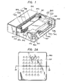
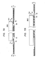
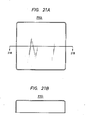
- Fug. 1 is a partially broken perspective view showing an overall magnetic bubbJe memory module of the present invention.
- Fig. 2A is a bottom view.
- Fig. 2B is a sectional view on line 2B-2B of Fig. 2A.
- Fig. 3 is an exploded perspective view showing a laminating structure.
- Fig. 4 is a view describing a substrate FPC.
- Fig. 5 is a plan view showing a substrate assembly BND where a chip DHI is loaded on the substrate FPC.
- Fig. 6 shows a view showing the chip CHI.
- Fig. 7 is a view describing lead bonding of the substrate assembly BND.
- Fig. 8 is a view describing a magnetic circuit PFC.
- Fig. 1 is a partially broken perspective view showing an overall magnetic bubbJe memory module of the present invention.
- Fig. 2A is a bottom view.
- Fig. 2B is a sectional view on line 2B-2B of
- FIG. 9 is a view describing a producing method of the magnetic circuit PFC.
- Fig. 10 is a view showing an inner case RFSb.
- Fig. 11 is a view showing an outer case RFSa.
- Fig. 12 is an assembly drawing of the case RFS.
- Fig. 13 is a sectional view showing an assembly case RFS in which the substrate assembly BND and the magnetic circuit PFC are accomodated.
- Fig. 14 is a view describing the construction of a magnet BIM.
- Fig. 15 is a view describing a bias coil BIC.
- Fig. 16 is a sectional voew showing an assembly of the case RFS with which a pair of magnets BIM and the bias coil BIC are incorporated.
- FIG. 17 is a view showing an outer shield case SHIa.
- Fig. 18 is a view showing an inner shield case SHlb.
- Fig. 19 is an assembly drawing showing a shield case SHI.
- Fig. 20 is a sectional view showing the assembly shown in Fig. 16 incorporated in the shield case SHI.
- Fig. 21 is a view showing a packaging case PKG.
- Fig. 22 is a view describing the construction of a terminal-fixing plate TEF.
- Fig. 23 is a view showing the construction of a contact pad CNP.
- Fig. 24 is a sectional view showing the chip CHI.
- Fig. 25 is a view showing the construction of a magnetic bubble detector D of the chip CHI.
- Fig. 26 is a view showing the construction of a magnetic bubble generator GEN of the chip CHI.
- Fig. 27 is a view showing the construction of a swap gate SWP of the chip CHI.
- Fig. 28 is a view showing the construction of a replicate gate REF of the chip CHI.
- Fig. 29A is a view showing the relation between a bias magnetic field Hb and a holding magnetic field Hdc.
- Fig. 29B is a view showing a'total revolving magnetic field Hr'.
- Fig. 30 is a view showing an overall circuit of a magnetic bubble board.
- Fig. 31 is a characteristic view showing a revolving magnetic field distribution.
- Fig. 32 shows a modified embodiment of a flexible substrate.
- Fig. 32 shows a modified embodiment of a flexible substrate.
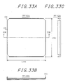
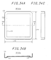
- FIG. 33 shows the inner case RFS2b, where Fig. 33A is a plan view, and Fig. 33B is a sectional view taken on the line 33B -33B of Fig. 33A.
- Fig. 34 shows the outer case RFS2a, where Fig. 34A is a plan view and Fig. 34B is a sectional view on the line 34B -34B.
- Fig. 35 shows the status of only the outer and inner cases RFS2a and RFS2b assembled together.
- Fig. 36 shows the status of the chip CHI, the flexible substrate FPC2, and the magnetic circuit PFC accommodated in the outer case RFS2a.
- Fig. 37 shows the magnet body BIM2, where Fig. 37A is a plan vies, Fig.
- Fig. 37B is a side view and Fig. 37C is a sectional view taken on the line 37C -37C.
- Fig. 38 shows the status of the magnet body BIM2 shown in Fig. 37 and the bias coil BIC shown in Fig. 15 accommodated in the case assembly RFS2 described with reference to Fig. 36, where Fig. 38A is a plan view and Fig. 38B is a sectional view taken on the line 38B -38B.
- Fig. 39 shows the upper shield case SHI2a, where Fig. 39A is a plan view, Fig. 39B is the right side view and Fig. 39C is the bottom side view.
- Fig. 40 shows the lower shield case SHI2b, where Fig. 40A is a plan view, and Fig.
- FIG. 40B is a lower side view.
- Fig. 41 shows the magnetic shield cases SH12a and SHI2b shown in Fig. 39 and Fig. 40 packaged therein with the intermediate assembly shown in Fig. 38, where Fig. 41 A is a plan view and Fig. 41 B is a sectional view taken on the line 41 B -41 B.
- Fig. 42 shows a substrate for electrically connecting the shield case assembly shown in Fig. 41 to the pin grid external connection terminal, where Fig. 42A is a plan view, Fig. 42B is a sectional view taken on the line 42B - 42B, and Fig. 42C is a bottom view.
- Fig. 43 shows the status when the shield case assembly shown in Fig.
- Fig. 41 is packaged on the pin grid substrate TEF2 shown in Fig. 42, where Fig. 43A is a plan view and Fig. 43B is a sectional view taken on the line 43B - 43B.
- Fig. 44 shows an encapsulation cap, where Fig. 44A is a plan view, and Fig. 44B is a sectional view taken on the line 44B -44B.
- Fig. 45 shows the finished structure of a series of modified embodiments described with reference to Fig. 32 thru Fig. 44, where Fig. 45A is a plan view, Fig. 45B is a sectional view taken on the line 45B -45B and Fig. 45C is a right side view.
- Fig. 45A is a plan view
- Fig. 45B is a sectional view taken on the line 45B -45B
- Fig. 45C is a right side view.
- Fig. 46 is a sectional view showing an assembly case RFS of a modified embodiment 2 of the present invention in which the substrate assembly BND and the magnetic circuit PFC are accomodated.
- Fig. 47 is a sectinal view showing an assembly case SHI of a modified embodiment 3 of the present invention.
- Fig. 48 is a sectional view showing an assembly case SHI of a modified embodiment 4 of the present invention.
- Figs. 1 and 2A and 2B are views for describing one embodiment of a magnetic bubble memory module according to the present invention.
- Fig. 1 is a partially broken perspective view.
- Fig. 2A is a bottom view thereof.
- Fig. 2B is a sectional view on the line 2B -2B of Fig. 2A.
- CHI denotes a magnetic bubble memory chip - (hereinafter, referred as to a chip).
- CHI denotes a magnetic bubble memory chip - (hereinafter, referred as to a chip).
- only one chip CHI is shown by deleting the other, but in the present embodiment, it is to be understood that two chips are disposed side by side. (It is possible to obtain more excellent chip yield ing by employing the construction wherein plural chips cover storage capacity conforming to a total of storage capacity than by employing one chip construction).
- FPC denotes a flexible aubstrate loaded on two chips CHI and having line group extensions for connecting between the chip CHI
- COI denotes a driving coil surrounding two chips CHI in the almost same level therewith and disposed to make the opposite side parallel with each other (hereinafter, referred as to a coil).
- COR denotes a picture frame core made of soft magnetic materials fixedly disposed so as to penetrate through a hollow portion of a square coil assembly COI (her q inafter, referred as to a core).
- This core COR and respective coils COI compose a magnetic circuit PFC for supplying an in-plane revolving magnetic field to the chip CHI.
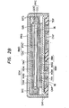
- RFS denotes a case for confining a revolving magnetic field which serves to accomodate a central square part of the substrate FPC and the while two chips CHI and magnetic circuit PFC - (hereinafter, referred as to a case).
- the case RFS is formed by working two dependent plates and the upper and the lower plates are electrically connected at the side sections of the case.
- RFS there is formed a drawn section around the case so as to narrow a gap of a central part in a somewhat wider range than the part on which the chip CHI is disposed. This drawn section can be utilized for positioning a magnet stated after.
- the case RFS has two effects, that is, functions of confinig a revolving magnetic field and mechanically supporting a weak substrate FPC.
- INM denotes a pair of inclined plates made of magnetic materials disposed at the outside of the case RFS.
- the thickness of the upper side of the inclined plate INM is gradually made larger toward the left and that of the lower side of the inclined plate INM is gradually made larger toward the right. Both plates form inclined surfaces at the side of the case RFS.
- Hc high permeability and small retentiveness
- Hc soft ferrite, Permalloy or the like
- soft ferrite is selected since it serves to facilitate working the inclined surfaces.
- MAG denotes a pair of permanent magnet plates disposed as putting each of them on the corresponding inside of a pair of inclined plates INM (hereinafter, referred as to a magnet plate).
- HOM denotes a pair of plates for homogenizing a magnetic field disposed as putting each of them on the corresponding inside of said each magnet plates and made of magnetic materials such as ferrite or the like.
- the magnet plate MAG is formed to wholly have an uniform thickness.
- INN denotes a pair of inclined plates disposed as putting each one of them on each corresponding inside plate of said plates for homogenizing a magnetic field and made of non-magnetic materials with excellent thermal conduc tivity.
- These inclined plates INN are formed to have the almost same gradient with that of the inclined plate INM and the inclined surfaces in the reverse directions to them.
- the inclined plate INM, the magnet plate MAG, the plate HOM for homogenizing a magnetic field and the inclined plate INN are disposed as piling them and integrated so as to compose a magnet body BIM for generating a bias magnetic field (hereinafter, referred as to a magnet body), when the magnet body composed of laminated plates is formed to uniformly have the overall thickness.
- a pair of magnet bodys BIM are attached on a central plane section surrounded by the drawn sections of the case RFS.
- bias coil BIC denotes a coil for generating a bias magnetic field disposed in a groove-like gap section between a peripheral portion of the magnet body BIM and the case RFS (hereinafter, referred as to a bias coil).
- the bias coil BIC is driven in case of arranging magnetism of the magnet plate MAG in accordance with the characteristics of the chip CHI or clearing all the bubbles of the chip CHI when there is accomplished the test as to fault of unnecessary-bubbles-generating.
- SHI denotes an outer magnetic shield case made of magnetic materials and for accomodating the case RFS in which the substrate loaded with said chip CHI and the magnetic circuit PFC are accomodated and, at the outside of the case, a pair of magnet bodys BIMa, BIMb and the bias coil BIC (hereinafter, referred as to a shield case).
- a shield case For the materials of the shield case SHI, it is preferable to employ the magnetic materials with high permeability u., large saturated flux density Bs and small retentiveness Hc.
- Permalloy or ferrite has such a characteristic, but the present embodiment selects iron-nickel alloy of Permalloy which is suitable for bending operation and can endure mechanical ex- temal force.
- RKC denotes a packaging case made of materials with high thermal conductivity and workability such as aluminum and mounted on the outer peripheral surface of said shield case SHI by attaching or engaging.
- CNP denotes a contact pad provided as extended from the four comers of said substrate FPC and disposed to be in contact with an outer connection terminal bent out to the rear surface of the shield case SHI.
- TEF denotes a terminal-fixing plate made of insulating materials and for fixedly supporting each contact pad CNP at an inter-stage portion of the opening.
- REG denotes resin mold agent enclosed at the inside four corners of the packaging case PKG and for fixing the assembly of the shield case SHl to the inside of the packaging case PKG.
- Fig. 3 is a perspective view as to assembling for describing the order of pile-assembling respective components composing the above-stated magnetic bubble memory module.
- the substrate assembly BND assembled by loading two chips CHI on the substrate FPC having connecting sections for input and output wirings projected at 4 corners and a chip-loading section at the central position is disposed in an outer case RFSa on which insulating sheets 36 are disposed by attaching.
- the substrate is filled with silicon resin STR (not shown).
- the inner case RFSb is engaged with the outer case RFSa and the side-contact portion between the outer case RFSa and the inner RFSb is electrically connected by means of soldering or the like.
- an upper magnet body BIMa and a lower magnet body BIMb are disposed on the concave drawn section provided on the outer surfaces of these outer case RFSa and the inner case RFSb and then the bias coil BIC wound in order is desposed on the gap (not shown) formed by an outer edge section of this upper side magnet body BIMa and the inside of the inner case RFSb.
- the outer shield case SHla and further the inner shield case SHlb is incorporated therewith.
- the side-contact portion between the outer shield case SHla and the inner shield case is electrically connected.
- the outer connection terminal-connecting sections of said substrate FPC projected at the four corners of the shield case SHI are bent to the rear surfaces of the inner shield case SHla as shown in Fig. 4B and are incorporated so as to have a fixed form.
- a terminal-fixing plate TEF loaded with contact pads CNP at respective openings is disposed in contact with respective outer connection terminals covered by soldering or the like respectively provided at said terminal-connecting sections .and respective outer connection terminals and the contact pads CNP are electrically connected with each other by means of soldering or the like.
- the assembly of them is accomodated in the packaging case PKG and the sealing such as hermetic sealing or the like is accomplished at the contact portions between the terminal-fixing plates TEF and the packaging case PKG so as to complete the assembling.
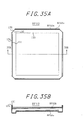
- Fig. 4 shows the substrate FPC.
- Fig. 4A is a plan view showing it.
- Fig. 4B is a plan view showing the connecting sections of the outer connection terminals projected at 4 corners, which are bent to the assembly.
- Fig. 4C is an enlarged sectional view taken on the line 4C -4C in Fig. 4A.
- Fig. 4D is an enlarged sectional view taken on the line 4D -4D in Fig. 4A.
- the substrate FPC includes a rectangular chip-loading section 1 at the central part, sections to be bent 2 (2a, 2b, 2c, 2d) whose widths are small at the four corners and rectangular outer connection terminal-connecting sections (hereinafter, referred as to a connecting section) 3 (3a, 3b, 3c, 3d), which are integrally formed so as to wholly have an almost windmill-like form.
- a connecting section 3a, 3b, 3c, 3d
- this chip-loading section 1 there are provided double-frame structure of square openings 4 (4a, 4b) to be loaded with the two chips CHI stated after and to be connected with the terminal sections thereof and three holes 5 (5a, 5b, 5c) for positioning and there is provided a projection 6 for positioning at the tip of the connecting section 3C.
- the patterns of lead wires 9a, circular outer terminals 9b, ellipsoidal coil lead-connecting terminals 9c, notes 9d, index marks 9e and the like as shown in Fig. 4A are formed by means of forming a copper thin film on a base film 7 made of a polyimide resin film with, for example, about 50 urn of thickness on which on epoxy system adhesive agent is coated as shown in Fig. 4C and then accomplishing etching of these films so as to form a required pattern. Further, a transparent or semi-transparent cover film 10 is attached and disposed on the upper surface of these films on which the adhesive agent 8 consisting of the same components with the above-stated agent is coated.
- an opening is formed on the base film 7 to be a chip CHI-loading side not shown in the drawings to tightly restricted dimensional tolerance. Then, an opening in relatively large dimensions is formed on an upper surface side cover film 10. Further, the lead wires 9a are exposed between the base film 7 and the cover film 10 and on the surface of these lead wires 9a, there is formed a tinning layer 11. Consequently, the opening form has a two-layered structure and at once a double-frame structure. On the other hand, in the connecting section 3, as shown in Fig.
- circular openings 12 are formed on the portions corresponding with said circular outer terminals 9b of the cover film 10 and elliptical outer terminals 9c not shown in the drawings and a soldering layer 13 by planting, dipping or the like is formed on the copper thin film patters of the outer terminals 9b and 9c exposed from the opening 12.
- respective outer terminals 9b and 9c provided at these connecting sections 3 are connected to respective lead wires 9a continuously formed on the chip-loading section 1, respective connecting sections 3a, 3b, 3c, 3d and respective bending sections 2a, 2b, 2c, 2d.
- lead wires 9a are aggregated as respective blocks of respective connecting sections 3a, 3b, 3c, 3d at a part of respective opening edges of respective openings 4a, 4b and these tips of respective blocks are exposed in respective openings 4a, 4b.
- the lead wire 9a of the connecting section 3a is disposed at the left upper part of the opening 4a.
- the lead wire 9a of the connecting section 3b is disposed at the left lower part of the opening 4b.
- the lead wires 9a of the connecting section 3c are disposed at the right upper part of the opening 4a.
- the lead wires 9a of the connecting section 3d are disposed at the right lower part of the opening 4b.
- this substrate FPC is constructed so as to easily discriminate those patterns by looking through the cover film 10, because, in the step stated after, respective connecting sections 3a, 3b, 3c, 3d are combined for engagement, as shown in Fig. 4B by bending respective sections to be bent 2a, 2b, 2c, 2d and respective outer terminals 9b, 9c on which the soldering layer 13 is formed are exposed to the surface and further, the surfaces of the lead wires 9a, the note 9d and the index mark 9e are covered by the cover film 10.
- the substrate FPC employs a polyimide resin film and is constructed to have a windmill-like form providing respective connecting sections 3a, 3b, 3c, 3d through respective sections to be bent 2a, 2b, 2c, 2d at the four comers of the chip-loading section 1.
- the chip-loading section 1 and the connecting sections are made to have two-layered wiring structures.
- the area of the chip-loading section 1 is made larger and at once the outer terminal section can be made to have plural terminals. Accordingly, the overall form can be minimized.
- Fig. 5 is a plan view showing the construction wherein the chip CHI is loaded on the above-stated substrate FPC.
- two chips CHI are loaded on the chip-loading section 1 of the substrate FPC as disposing them between the openings 4a, 4b in parallel so as to complete the substrate assembly BND.
- One of the chips is constructed by integrating two blocks of 1 Mbit as shown in an enlarged plan view of Fig. 6.
- two chips CHI have four blocks, that is, totally compose a 4 M bits chip.
- a large line shows a conductor pattern and a thin line shows a chevron pattern propagation path.
- a gold bump 15 is loaded by means of the lead-bonding using Au-Sn eutectic crystal caused by a pressure melding method as disposing a gold bump 15 between respective bonding pads 14 provided by gold-planting at the end of the chip CHI and the wiring leads 9a on which the tinning layer 11 is formed in the opening 4 of the substrate FPC as respectively shown in enlarged sectional views of Figs. 7A and ' 7B.
- the chip CHI it is possible to fixedly support the chip CHI by connecting the lead wires 9a in the openings 4a, 4b of the substrate FPC with the bonding pads 14 of the chip CHI by means of the lead-bonding using Au-Sn eutectic crystal. Accordingly, it is possible to greatly ameliorate strength for connection and thin the construction. Further, the surface of the chip CHI is covered by the chip-loading section 1 of the substrate FPC. Thus, the surface of the chip CHI is protected and at once it is possible to ameliorate handling efficiency and to hold mechanical strength of the substrate FPC.
- each chip CHI consists of two blocks and two chips CHI are composed of 4 blocks
- respective blocks can be distributively connected to respective connecting sections 3a, 3b, 3c, 3d which are the closes to respective blocks and thus the symmetric position of the chips CHI can be obtained so as to extremely facilitate a test, a check and the like.
- the substrate FPC provides four connecting sections, 3a, 3b, 3c, 3d, it is possible to give and receive an input and an output signals having least noise by means of separating wirings for magnetic bubble detectors DET, map loops of each chip CHI and the like from the other wiring functions and aggregating them at one connecting section (refer to Fig. 6) and selectively disposing this connecting section at the location which is far away from a noise-generating source.
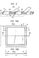
- Fig. 8 shows the magnetic circuit PFC.
- Fig. 8A is a perspective view.
- Fig. 8B is a plan view showing the driving magnetic circuit.
- a coil COI composed of four coils 20a, 20b, 20c and 20d by providing - wirings (in the arrow direction are provided on the parallel sides facing to each other of the picture frame type of core COR made of soft magnetic materials and a X-coil 22a is composed by accomplishing series winding of the coils 20a and 20b on the sides facing to each other by way of a contact 21 b and a Y-coil 22b is composed by accomplishing series winding of the coils 20c and 20b by way of a contact 21 a.
- leakage magentic fields Hx and Hy are respectively generated in the x-axial direction and in the y-axial direction so as to supply the above-stated two chips CHI with them as a revolving magnetic field.
- the magnetic circuit PFC constructed as stated above is completed by the step of, as shown in a perspective view of Fig. 9, providing windings in a rectangular parallelepiped-like magnetic core 23 made of one soft magnetic material and a tap 24 at each plural blocks, forming a pair of coils, for example, a pair of X-coils 22a composed of the coils 20a, 20b, by accomplishing series winding and providing a wider groove 25 and a less wide groove 26 respectively having fixed widths between respective coils 20a and 20b by means of cutting work, afterwards, engaging the wider grooves 25 divided into two parts at the center of this less wide groove 26 with each other rectangularly and attaching them so as to buildup a picture frame type of core as shown ia Fig. 8.
- the rectangular parallelepiped core 23 forming the above-stated wider groove 25 and less wide groove 26 in advance can provide the coil 20a and the coil 20b by way of the tap 24 so as to form a pair of X-coils 22a.
- the above-stated pair of Y-coils 22b can be formed quite similarly with the X-coils.
- the rectangular parallelepiped core 23 provides the coils 20a, 20b as providing the tap in the series direction, in case of completing the construction by assembling as shown in Fig. 8, there is no need to connect lines (contact) as crossing them with each other and thus it is possible to simplify winding.
- this magnetic circuit PFC is made to have a picture frame type of structure and thus is not disposed on the upper or the lower surface of the chip CHI. Thus, the thickness in the lamination direction is made smaller and thus the thinning of the circuit can be realized.
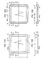
- Fig. 10 shows the inner case RFSb.
- Fig. 10A is a plan view.
- Fig. 10B is a sectional view taken on the linelOB -10B of Fig. 10A.
- the inner case RFSb is built up of a frame type of drawn section 30 providing a concave portion at its center, bent sections 31 made by bending a pair of opposite side edges to each other upwardly about 90° and cut-away sections 32 made by cutting respective four comers in the slanting direction.
- This case RSFb is formed by press working of excellent conducting materials, for example, an oxygen free copper plate.
- the drawn section 30 and the bent sections 31 have a function of ameliorating mechanical strength of this inner case RFSb in the spiral direction and at once to suitably restrict outer length L in the vertical and transversial directions between each opposite bent sections 31 to each other.
- the drawn section 30 can suitably arrange the distance between the magnet body BIMb disposed at the outer surface sides of this case RFSb and the chip CHI disposed at the inner surface side thereof.
- the cut-away sections 32 provided at the four corners form the drawing section of respective sections 2a, 2b, 2c, 2d to be bent of the substrate FPC disposed in this case RFSb.
- oxygen free copper is employed but it is possible to employ copper, silver, or gold plate or the plate made by planting the alloy plate of these materials.
- Fig. 11 shows the outer case RFSa corresponding with the above-stated inner case RFSb.
- Fig 11 A is a plan view.
- Fig. 11 B is a sectional view taken on the line 11B -11B.
- this outer case RFSa is produced by using the same materials and manufacturing method with the above-stated inner case RFSb. It is comprised of a frame type of drawing section 33 providing a concave portion at its center, bent sections 34 made by bending two pairs of opposite side edges upwardly about 90° and cut-away sections 35 made by cutting away respective four comers in the slanting direction, similarly with the above-stated case.
- two pairs of bent sections 34 are formed to have the almost same inside length between the opposite bent sections with the outside length L between the corresponding opposite bent sections of said inner case RFSb and higher height H than those of said inner case RFSb.
- these drawn section 33 and cut-away sections 35 are formed to have the almost same dimensions with those of said inner case RFSb.
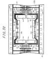
- the outer case RFSa and the inner case RFSb as constructed above are assembled to be an integrated case RFS by means of inserting the inner case RFSb into the outer case RFSa and connecting them with each other to make the inner case RFSb be in contact with the outer surfaces of the bent sections 31 of the outer case RFSa, as shown in Fig. 12A which is the plan view of the case RFS and in Fig. 12B which is the sectional view taken on the line 12B -12B of Fig. 12A.
- Fig. 13 is a sectional view showing the above-stated case RFS and the substrate assembly BND accomodated and disposed in said case.
- the outer case RFSa for example, about 0.1 mm of thickness of poIyimid film 36 is disposeed and attached as an electrically insulating sheet.
- the substrate assembly BND and the magnetic circuit PFC are respectively disposed on this film 36 and the peripheral portion thereof.
- an epoxy system adhesive agent 37 is coated on the upper surface of the substrate assembly BND and then, in the upper part of them, the inner case RFSb is inserted, disposed and joined.
- the inner surfaces of the bent sections 34 of this outer case RFSa are mechanically and electrically jointed with the outer surfaces of the bent sections 31 of the inner case RFSb at the portions marked by X by means of metal flowing, soldering or the like.
- Silicon resin SIR fills in the with the outer surfaces of the bent sections 31 of the outer case RFSa, as shown in Fig. 12A which is the plan view of the case RFS and in Fig. 12B which is the sectional view taken on the line 12B -12B of Fig. 12A.
- Fig. 13 is a sectional view showing the above-stated case RFS and the substrate assembly BND accomodated and disposed in said case.
- the outer case RFSa on the bottom of the outer case RFSa, for example, about 0.1 mm of thickness of polyimid film 36 is disposeed and attached as an electrically insulating sheet
- the substrate assembly BND and the magnetic circuit PFC are respectively disposed on this film 36 and the peripheral portion thereof.
- an epoxy system adhesive agent 37 is coated on the upper surface of the substrate assembly BND and then, in the upper part of them, the inner case RFSb is inserted, disposed and joined. In this instance, the inner surfaces of the bent sections 34 of this outer case RFSa are mechanically and electrically jointed.
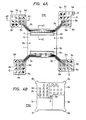
- Fig. 14 shows the magnet body BIM.
- Fig. 14A is a plan view thereof.
- Fig. 14B is a side view thereof.
- Fig. 14C is an elevational view thereof.
- the magnet body BIM is formed by piling up an inclined plate INN made of non-magnetic materials such as copper and having one predetermined inclined surface of the opposite surfaces, a plate HOM for homogenizing a magnetic field whose thickness is uniform and to be disposed at the inclined surface side of this inclined plate INN, a magnet plate MAG whose thickness is uniform and to be disposed at the upper surface side of this plate for homogenizing a magnetic field HOM and an inclined plate INM havong.an inclined surface and to be disposed at the upper surface side of this magnet body MAG and then integrating them by means of an epoxy system adhesive agent.
- an inclined plate INM havong.an inclined surface and to be disposed at the upper surface side of this magnet body MAG and then integrating them by means of an epoxy system adhesive agent.
- Fig. 15 shows a bias coil BIC.
- Fig. 15A is a perspective view thereof.
- Fig. 15B is a sectional view taken on the line 15B -15B of Fig. 15A.
- the bias coil BIC is formed to be a pciture frame type having a predetermined value by means of providing windings in order 40 on which, for example, thermosetting resin is coated as an insulated member so as to be disposed as 5 X 4 windings in section and to make the overall form picture frame-like and then pressure-melding the windings by thermal deposition and cooling it.
- the bias coil is formed by thermal- depositing thermosetting resin coated on the outer surfaces of respective windings 40 and loading respective windings 40 and loading respective windings 40 by pressure-welding. Then, by cooling it, respective windings 40 are hardened in the united state of windings and thus having a predetermined picture frame.
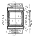
- Fig. 16 is a sectional view showing the case RFS desoribed in Fig. 13, the above-stated magnet body BIM and bias coil BIC incorporated in the case.
- an upper magnet body BIMa and a lower magnet body BINb are respectively disposed and jointed on the upper and the lower surfaces of the case RFS assembly accomodated in the substrate assembly BND and the magnetic circuit PFC.
- the bias coil BIC is accomodated and disposed in a picture frame groove section formed by being surrounded by the peripheral portion of this upper magnet body BIMa and the bent sections of the inner case RFSb.
- the upper magnet body BIMa and the lower magnet body BIMb are formed by means of the same materials and in the same dimensions with each other.
- magnet bodys BIMa and BIMb at their inclined plate INN sides are respectively disposed closely in a concave portion surrounded by the drawn section 30 of the inner case RFSb and a concave portion surrounded by the drawn section 33 of the outer case RFSa.
- the construction described above it is possible to dispose a pair of magnet bodys BIMa and BIMb in the concave portions formed at both surfaces of the central part of the case RFS assembly and further provide the bias coil BIC in the picture frame groove formed in the peripheral section of those magnet bodys.
- the overall thickness of each component in the laminating direction is made smaller and the miniaturizing and thinning of the construction can be realized.
- the picture frame space groove is formed by the outer case RFSa and the peripheral portion of the upper magnet body BIMb, it is possible to dispose the above-stated bias coil BIC in this space groove, to newly provide a bias coil and further to form a bias coil by accomplishing windings as using the groove as a coil bobbin.
- Fig. 17 shows an outer shield case SHla.
- Fig. 17A is a plan view thereof.
- Fig. 17B is a sectional view taken on the line 17B -17B of Fig. 17A.
- the outer shield case SHla is comprised of a flat section 51, bent sections 52 made by bending two pairs of opposite side edges of the flat section 51 upwardly about 90°, concave portion 53 made by cutting away part of the central parts of these bent sections 53 and cut-away sections 54 made by cutting respective four comers of these bent sections in the slanting direction.
- This outer shield case SHla has high Permeability and saturated flux density and it should be preferably formed by press-working materials with high thermal conductivity, for example, a Permalloy plate.
- Fig. 18 shows an inner shield case SHIb corresponding with the above-stated outer shield case SHla.
- Fig. 18A is a plan view thereof.
- Fig. 18B is a sectional view taken on the line 18B -18B of Fig. 18A.
- this inner shield case SHlb is formed by the same materials and manufacturing method with the outer shield case SHla stated above. It is comprised of, similarly with the above, a flat section 55, sections 56 made by bending two pairs of opposite side ends upwardly about 90°, concave portions 57 made by cutting away part of the central parts of these bent sections 57 and cut-away sections 58 made by cutting respective corners or these bent sections.
- each opposite bent sections 56 have the almost same outside length betweeen them with the inside length L4 between each opposite bent sections 52 of the above-stated outer shield case SHla and the height H of the inner shield case SHlb is lower than that of the outer shield case SHIa.
- Fig. 19A is a plan view showing the outer shield case SHla and the inner shield case SHlb constructed above.
- Fig. 19B is a sectional view taken on the line 19B -19B.
- the shield case SHI is integrally built up by means of inserting the inner shield case SHlb in the outer shield case SHla and accomplishing spot-welding or solder-welding in relation to the concave portion 59 formed by the concave portion 53 of the outer shield case SHla and the concave portion 57 of the inner shield case SHIa so as to magnetically and mechanically fix both shield cases with each other.
- Fig. 20 is a sectional view showing the above-stated shield case SHI assembly, the case RFS assembly incorporating the substrate assembly BND and the magnetic circuit PFC therein as described in Fig. 16 and the assembly consisting of a pair of magnet body BIMa and BIMb and the bias coil BIC respectively incorporated in said shield case SHI assembly.
- the upper magnet body BIMa at the bottom to the center, the bias coil BIC at the peripheral portion, the case RFS assembly - (incorporating the substrate assembly BND, the magnetic circuit PFC and the like therein), the lower magnet body BlMb are sequentially laminated and disposed and then the inner shield case SHIb is inserted to the outer shield case.
- both shield cases are sealed with each other by means of welding the concave portion 59 (refer to Fig. 19) formed by the concave portion 53 of the outer shield case SHla and the concave portion 59 of the inner shield case SHlb stated above.
- the concave portion 59 (refer to Fig. 19) formed by the concave portion 53 of the outer shield case SHla and the concave portion 59 of the inner shield case SHlb stated above.
- Fig. 21 shows a packaging case PKG.
- Fig. 21 A is a plan view thereof.
- Fig. 21 B is a sectional view taken on the line 21 B -21 B.
- the packaging case PKG can be formed by means of accomplishing the drawing to the materials with excellent thermal conductivity, for example, an aluminum plate whose thickness is about 0.5 mm.
- a black coat (not shown) is provided on the outer surface of the case. It is possible to utilize the above-stated outer shield case SHla as a packaging case PKG by improving the form of said outer shield case.
- this packaging case PKG serves as an outer case given after completion of a magnetic bubble memory module and has a function as a dissipating member. Besides, the inside corner sections thereof has a function as a mold in case of resin molding by means of a potting method stated after.
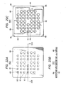
- Fig. 22 shows a terminal-fixing plate TEF.
- Fig. 22A is a plan view thereof.
- Fig. 22B is a sectional view taken on the line 22B -22B.
- Fig. 22C is a rear elevation thereof.
- the terminal-fixing plate TEF is made of electrically insulating mateirqls, for as a glass epoxy system resin plate 60 and is formed to have such length arid breadth as to freely put in or out of said packaging case PKG. And, on the surface of this resin plate 60 except its peripheral portion, a plurality of through holes 61 are provided in matrix arrangement with a predetermined interval in the breadth and length direction.
- a non-through hole 62 which is rotationally symmetric and has a concave in section is provided. There is attached a mark 63 such as a white coat for indicating direction or distinction in this non-through hole 62.
- a plurality of through holes 61 provided in this resin plate 60 provide openings 64 with a large diameter axially connected with through holes at the rear side of the resin plate as shown in Fig. 22B. These openings 64 all have depth of about 60% of the plate thickness and are respectively connected with the through holes 61 as having steps on the way of connection.
- this resin plate 60 there is formed along the peripheral portion a groove 65 which has the almost same depth with the depth of said openings, different width in- the horizontal direction therefrom and a concave state in section.
- the inside of this groove 65 serves as the passage section and the connection section of the coil COI windings and the bias coil BIC windings stated above,
- the corner portions of this resin plate 60 are not formed as concave forms. They have a predetermined plate thickness and serve as contact surfaces to the inner side surfaces of the above-stated packaging case PKG.
- the rear side of the resin plate 60 is formed to have a two-stepped structure which, namely, has two thicknesses.
- Fig. 23 shows a contact pad CNP.
- Fig. 23A is a plan view thereof.
- Fig. 23B is a sectional view thereof.
- the contact pad CNP is formed by means of accomplishing pressing work of good conducting materials, for example, a copper plate whose thickness is about 0.5 mm to punch out a piece member 70 and then forming a nickel-planting layer 71 and a gold-planting layer 72 on the surface of the piece member 70.
- the shield case assembly described in Fig. 20 is inserted to the packaging case PKG stated above.
- respec tive connecting sections, 3a, 3b, 3c, 3d of said substrate assembly BND (refer to Fig. 4A) are projected from the four corners of this packaging case PKG as bent at about 90 degrees on the basis of respective sections to be bent 2a, 2b, 2c, 2d.
- respective components are fixedly disposed in this packaging case PKG by accomplishing a resin-molding to the four corners of this packaging case PKG by means of a potting method.
- these connecting sections 3a, 3b, 3c, 3d are respectively bent about 90 degrees by the corresponding sections to be bent 2a, 2b, 2c, 2b and then are engaged on the outer surface of the inner shield case SHlb shrough an adhesive agent as shown in Fig. 4B. Then, the contact pads CNP are loaded in respective openings provided on the rear side of said terminal-fixing plate TEF or the sides of the contact pad CNP are made solid by means of an adhesive agent and then the treated contact pads CNP are inserted in the packaging case PKG so as to be disposed in contact with respective connecting sections 3a, 3b, 3c, 3d.
- the arrangement pitch of respective external terminals 9b provided on respective connecting sections, 3a, 3b, 3c, 3d corresponds with the arrangement pitch for respective contact pads CNP.
- resepctive external terminals 9b are electrically in contact with the contact pads CNP.
- a heated thing whose tip is slender or something like that is inserted to each through holes 61 from the rear side of the disposed terminal-fixing plate TEF so as to attach the contact pads CNP with the external terminals by pressure welding. Consequently, respective external terminals 9b are electricaly connected with the corresponding contact pads CNP and at once the terminal-fixing plate TEF is mechanically fixed to the contact pads so as to complete the magnetic bubble memory module as shown in Fig. 2.
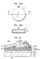
- Fig. 24 is a sectional view showing the portion around the bonding pad PAD of the magnetic bubble chip CHI stated above.
- GGG - (gadolinium -gallium -gamet) denotes a substrate.
- LPE denotes a bubble magnetic film formed by means of a liquid phase epitaxial growth method.
- Table 1 One example of its composite is referred in the following Table 1.
- INO denotes an ion-implanted layer formed on a LPE film surface for restraining hard bubbles.
- SP1 denotes a first spacer which serves to form, for exampie, SiO 2 whose thickness is 3000A by means of a gaseous phase chemical reaction.
- CON 1 and CON 2 denote two conducting layers and has a function of controlling generation of bubbles, duplication (division) thereof and exchanging thereof as stated above.
- a lower first conducting layer CON 1 and an upper second conducting layer CON 2 are respectively made of materials such as Mo and those such as Au.
- SP2 and SP3 respectively denote layer-insulating films (a second and a third spacers) made of polyimide resin or the like for performing electrical insulation between the conducting layers CON and a transfer pattern layer P made of Permalloy or the like formed thereon.
- PAS denotes a passivatopn film formed out of a Sio,-film or the like formed by means of a gaseous phase reaction method.
- PAD denotes a bonding pad of the chip CHI, where a fine connector wire such as a At-wire or the like is bonded by means of a pressure welding method or a supersonic method.
- a lower first layer PAD 1, a middle second layer PAD 2 and an upper third layer PAD 3 are respectively formed out of materials such as Cr, those such as Au and those such as an Au-planting layer. It is possible to form the second and the third layers PAD 2 and PAD 3 out of the materials such as Cr, Cu or the like.
- P denotes the layer utilized as a transfer path of bubbles, a dividing, a generating, an exchanging and a seraching sections of bubbles and a guardrail section. In the description stated after, it is described as a transfer pattern layer for convenience' sake.
- this transfer pattern layer P employs Fe -Ni as a lower layer P1 and an upper layer P2, but it is possible to exchange both materials with each other as stated before.
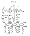
- Fig. 25 shows a D section of a bubble detector.
- MEM denotes a main magnetic resistance element for detecing the existence of bubbles by means of variation of a resistance value provided in case of passing the bubbles extended like a band in the lateral direction through the element.
- MED denotes a dummy magnetic resistance element having the same pattern form with those of the main magnetic resistance element and is utilized for detecting noise components brought about by the influence of a revolving magnetic field and the like.
- MEM main magnetic resistance element
- PR denotes the transfer direction of bubbles.
- ER denotes a bubble eraser and serves to erase bubbles when they attain to the conducting layer CND.
- the guardrail GR consisting of pattern blocks lining up in three files is provided around this detector D and between the dummy and the main detections and serves to get the unnecessary bubbles generated in the inside of the guardrail GR out of the guardrail and to prevent entering the unnecessary bubbles generated in the outside of the guardrail GR into the inside thereof.
- the patterns except the conducting layer CND pattern show the transfer pattern layer P described in Fig. 24.
- a signal-to-noise ratio (S/N ratio) is ameliorated by means of forming the magnetic resistance elements MEM and MED by a multilayered magnetic layer.
- the efficiency of the guardrail GR can be improved because of heightening a discharging factor for unnecessary bubbles by means of reducing retentiveness Hc.
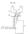
- Fig. 26 shows a magnetic bubble-generator GEN.
- the current generated in the magnetic bubbles can be made smaller by making the transfer pattern layer P multilayered and thus it is made possible to lengthen the life of the conducting layer CND of the magnetic bubble-generator. Accordingly, the driving circuit for the conducting layer CND can employ a semiconductor element with a small current capacity value and thus its cost can be made lower.
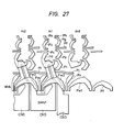
- Fig. 27 shows a minor loop m composed of transfer patterns such as Pa -Ph and the like, a write major line WML composed of the transfer patterns such as Pw, to Pw 3 and the like and a swap gate section composed of a hairpin conducting layer CND.
- P7 is the same with the transfer pattern P7 in the bubble-generator GEN shown in Fig. 26.
- the bubbles generated in the bubble-generator GEN are transferred to the write major line WML through the P1 to P7 transfer pathes.
- the magnetic bubbles in the transfer pattern Pd of the minor loops ml are transferred through the transfer patterns Pt and Pm to the transfer pattern Pw3 of the major line WML and the magnetic bubbles from the major line PW1 are transferred through the transfer patterns Pk, Pj and Pi to the transfer pattern Pe of the minor loop in order to accomplish an exchange of bubbles, that is, informations with each other.
- the swap gate is not provided in the minor loop md at the right end, because it is a dummy loop where magnetic bubbles are not injected for reducing a peripheral effect. As described above, it is possible to accomplish an exchange of magnetic bubbles with a small current value by means of making the transfer pattern layers Pi to Pm at the exchange location multilayered.
- the magnetic bubbles are usually transferred on the route of Pn to Pg and Ps to Px.
- the conducting layer CND is energized, the bubbles is divided at the location of the transfer pattern Pg and one divided magnetic bubble is transferred to a read major line RML by way of Py and P8 to P10.
- the magnet body MAG is disposed as about 2 degrees tilted in relation to the chip CHI. This is designed to apply a bias magnetic field Hb to the chip CHI in the direction a little shifted from the vertical. Thus, it is possible to generate a holding magnetic field Hdc for ameliorating a atart and a stop margins of the bubble transfer to raise about 6(Oe)(Fig. 29A).
- the series magnetic field Hz is made to have a component Hdc on the xy plane.
- the direction of this in-plane component Hdc is slanted to coincide with the start and stop (St/Sp) direction in the revolving magnetic field Hr(+ x-axis direction).
- This component Hdc on this xy plane is a well-known magnetic field effectively served as the start and stop (St/Sp) operation of the revolving magnetic field Hr and called as a holding field. Further, magnitude of the bias magnetic field Hb vertically functioned on the chip CHI plane is made to be Hz•cos ⁇ .
- Hr denotes a revolving magnetic field applied from the external.
- Hr' denotes a revolving magnetic field functioning to the chip CHI.
- the revolving magnetic field Hr' functioning to the chip CHI is made to be a synthesis of the revolving magnetic field Hr applied from the external and the in-plane component Hdc and the center O' of the revolving magnetic field Hr' is shifted in parallel by the in-plane component Hdc in the start and stop (St/Sp) direction, that is, + x-axis direction.
- the intensity of the revolving magnetic field Hr applied from the external is
- of the revolving magnetic field effectively functioning to the chip CHI is variable in accordance with the phase of the revolving magnetic field Hr.
- in the St/Sp direction is made to be
- Hr' in the opposite direction to the St/Sp direction is made to be
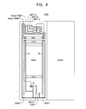
- RF denotes a circuit for generating a revolving magnetic field Hr by flowing the current whose phase difference is 90 degrees through the X-and Y-coils of the chip CHI.
- SA denotes a sense amplifier for sampling a minute bubble-detecting signal from the magnetic resistance element of the chip CHI in accordance with a timing of the revolving magnetic field, sensing and amplifying it.
- DR denotes a driving circuit for generating the bubbles in relation to the write in the magnetic bubble memory device MBM, flowing current through respective replicate functioning conductors in relation to swapping and reading in accordance with a predstermined timing and driving a bias coil BIC.
- the above-stated circuits are synchronized by means of a timing-generator TG so as to be operated in synchronization with a cycle and a phase angle of the revolving magnetic field Hr.
- Fig. 32 shows the embodiment wherein two rectangular connecting sections 3a, 3b are extended from the upper side of a chip-loading section 1 in the right and the left directions and bent by the sections 2a, 2b.
- Fig. 33 shows the embodiment wherein two Y-like connecting sections 3a, 3b are extended in the diagonal line direction and are bent by the sections 2a, 2b.
- Fig. 34 shows the embodiment wherein there is employed a wholly rectangular substrate FPC providing connecting sections 3a, 3b on the right side and the left side and these sections are bent by the sections 2a, 2b.
- Fig. 35 shows the embodiment wherein four chips are loaded on a wholly cross- shaped substrate FPC and of four connecting sections 3a, 3b, 3c, 3d provided at respective tips of the substrate, two pairs of opposits connecting sections are respectively bent on the upper surface and the lower surface of the module.
- the connecting sections 3a, 3b are bent to the upper surface of the module by the sections 2a, 2b and the connecting sections 3c, 3d are bent to the lower surface of the module by the sections 2c, 2d and thus the substrate FPC has a three-layered structure as a whole. Further, in the embodiments shown in Figs.
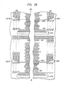
- the present invention is designed to dispose the magnetic bubble memory chip loaded with the flexible substrate in the space section of the revolving magnetic circuit consisting of a picture frame core and to lay the overall body for confining a revolving magnetic field within the case, the body being made of good conducting materials, and to electrically connect the peripheral portion of the overall body with the case.
- a highly uniform revolving magnetic field can be obtained by a small Vl product because of reducing the space for generating a leakage magnetic field and the magnetic ' bubble memory module which is designed to lower power consumption, miniaturize and thin the overall form and ameliorate assembling efficiency can be obtained because of miniaturizing the case for confining a revolving magnetic field.
- Fig. 32 shows a modified embodiment of a flexible substrate.
- the flexible substrate FPC2 differs from that shown in Fig. 4 in such points as follows:
- the substrate FPC2 has a copper foundation lead wire pattern which is formed by means of patterning with etching technique the copper film which is lined with epoxy system adhesive onto the base film composed of a polyimide resin film having the thickness of approsimately 50nm.
- a Ni-plating layer and an Au-plating layer are formed successively by the electroplating method, etc.
- This Au-plating layer is provided for the purpose of preventing from the electrical migration of the copper layer or making the thermocompression bonding of the magnetic bubble memory chip CHI with the bonding pad easy.
- the Ni layer is used for the purpose of improving adherence between the copper layer and the Au- layer.
- the lead wire patten 100 of each frame is connected at this stage by the frame-shaped pat- tem provided along the periphery shown in the drawing and the estended portion 100e, but it is for electroplating.
- the external connection parts 100c of lead wire 100 are concentrated in two directions as previously described.
- One of the reasons for the concentration in the left and right directions instead of upward and downward directions is to obtain compatibility with the 35mm film described above.
- Another reason is as follows.
- the memory chip CHI is face-up bonded underneath the film substrate FPC2, but the substrate FPC2 and the chip CHI are inclined in left and right directions in the drawing as described later. (Under the same bias condition as Fig. 2B, inclination toward the right is arranged such that the left side is high and the right side is low with the magnet body as the reference.)
- the substrate FPC2 is not inclined in upward and downward directions. Therefore, when the film substrate and the chip CHI is electrically connected after bonding.
- Fig. 33 shows the inner case flFS2b.
- Fig. 33A is a plan view
- Fig. 33B is a sectional view taken on the line 33B -33B of Fig. 33A.
- This case RFS2b is different from that shown in Fig. 10 in such points that the drawing section is omitted and the bottom plate thickness gets thicker as getting closer to the righthand side.
- the lower surface of the bottom plate is tapered lowering toward the right at an angle of 1.7 degree against the upper surface.
- a plate HOM for homogenizing a magnetic field and the magnetic body of a permanent magnet are provided on the upper surface and the chip CHI is arranged on the lower surface.
- the inclination of thickness is provided for the purpose of giving to the chip CHI a holding magnetic field Hdc due to the inclination between the magnetic body and the chip CHI.
- the inclined surface of the conductor case described above is formed by means of press work with about 300 tons (inclined padding process). As other forming method, such inclined surface may be formed either by cutting or by tilting a roller during rolling process.
- Fig. 34 shows the outer case RFS2a.
- Fig. 34A is a plan view and Fig. 34B is a sectional view on the line 34B - 34B.
- the difference of the outer case RFS2a from the inner case RFS2b exists in that it has a drawing section 133 for containing or fitting the magnetic core PFC.
- a tapered surface lowering to the right which is similar to the lower surface of the bottom plate or the inner case RFS2b is provided.
- Fig. 35 shows the status of only the outer and inner cases RFS2a and RFS2b assembled together (The chip CHI, the film substrate FPC2 and the magnetic core PFC are omitted in the drawing in the same way as Fig. 12).
- Fig. 12A is a plan view and Fig. 12B is a sectional view taken on the line 35B -35B.
- Fig. 36 shows the status of the chip CHI, the flexible substrate FPC2, and the magnetic circuit PFC accommodated in the outer case RFS2a (the status before covering up with the inner case RFS2b).
- Fig. 36A is a plan view and Fig. 36B is a sectional view taken on the line 36B -36B.
- the chip CHI is mounted on the substrate before being accommodated in the case RFS2a.
- the chip CHI is mounted on the back of the flexible substrate FPC2 keeping the main surface up (face up), on which bonding pads, lead wires and the transport path are located. It is needless to say that connection is made at the lead wire part 100a of the substrate FPC2 and the pad area of the chip CHI, but both are bonded by means of thermocompression of the lead wire part 100a on the pad with toolings such as a capillary.
- the film substrate 101 consisting of plurality of substrates FPC2 is separated into individual substrate FPC2, and unnecessary lead wire parts and reinforced area which were used in plating the periphery are cut off as shown in Fig. 36A.
- the conductor case RFS2a is applied with adhesives such as epoxy system resin by a stamping method, where the back of the chip CHI which was bonded on the film substrate FPC2 is adhered.
- the relation at this time between the locations of the chip CHI and the case RFS2a can be determined precisely by means of the cut-away section 135 of the case RFS2a and external connecting sections 102a thru 102d. If necessary, more fine positioning adjustment is feasible by using jigs, etc.
- the magnetic circuit PFC is housed in the groove formed by the drawing section 133 of the case RFS2a and the outside wall 134.
- potting with silicone resin REG2 is performed around the chip CHI.
- the selicon resin REG2 increases its fluidity by heating treatment and gets into between the back of the flexible substrate FPC2 and the main surface of the chip CHI by means of the capillary action, thereby protecting the chip CHI against adhesion of dust and permeation of moisture.
- the height of the case RFS2a at the drawing section 133 is determined so that the flexible substrate FPC2 will be flat all over the inside of the case as shown in Fig. 36B taking the thickness of the magnetic circuit FPC and the thickness of the chip CHI into consideration. Thereafter, the case RFS2b is welded by the ultrasonic welding method at its surface contact part with the case RFS2a.
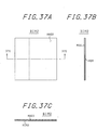
- Fig. 37 shows the magnet body BIM2.
- Fig. 37A is a plan vies
- Fig. 37B is a side view
- Fig. 37C is a sectional view taken on the line 37C -37C.
- the magnet body BIM 2 shown differs from that (BIM) shown in Fig. 14 in such a point that inclined plates INM and INN are omitted.
- Fig. 38 shows the status of the magnet body BIM2 shown in Fig. 37 and the bias coil BIC shown in Fig. 15 accommodated in the case assembly RFS2 described with reference to Fig. 36.
- Fig. 38A is a plan view and Fig. 38B is a sectional view taken on the line 38B -38B.
- the upper magnet body BIM2a and the bias coil BIC are mounted on the plate-shape inner case RFS2b, and the lower magnet body BIM2b is mounted on a flat part surrounded by the drawing section 38 of the outer case RFS2a.
- the chip CHI and the magnetic circuit PFC are inclined in left and right directions with reference to a parallel surface formed by upper and lower magnet bodies BIM2a and BIM2b.
- the condition for arranging the magnetic circuit PFC and the chip CHI in parallel remains unchanged from those embodiments shown in Fig. 13 and Fig. 16, but the thickness of the chip CHI, the thickness of the magnetic circuit PFC and the height of the drawing section 38 of the outer case RFS2a are designed so that the uppermost end surface of the magnetic circuit PFC and the upper surface of the chip CHI are almost even with each other, thereby preventing from application of the stress to the flexible substrate FPC2.
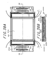
- Fig. 39 shows the upper shield case SHI2a
- Fig. 39A is a plan view
- Fig. 39B is the right side view
- Fig. 39C is the bottom side view.
- the plane figure of the upper shield case SHl2a is square in shape and is symmetrical for any axis of four center lines passing the same point (not shown), horizontal, vertical, and going up and down at 45° toward the right.
- the cut-away sections 154 at four cormers making a right angle with the 45° center lines are provided for the purpose of having lead wire portions 102a thru 102d pass through at the four comers of the film substrate FPC shown in Fig. 32.
- 151 denotes the plane section of the case
- 152 denotes the upright wall section.
- Protruded sections 152a thru 152d are provided at the center part of each side of the walls 152.
- the height of protruded sections 152a and 152c on left and right sides is to be h 2
- the height of protrusion itself (h 2 -h,) is to be the same as the thickness to of the lower shield case SHI2b shown in Fig. 40.
- the height of the protruded sections 152b and 152d on upper and lower sides is to be h 3
- the height of protrusion itself (h 3 -h,) is to be slightly bigger than the thickness to of the lower shield case SHI 2 b.
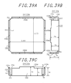
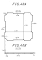
- Fig. 40 shows the lower shield case SHI2b.
- Fig. 40A is a plan view
- Fig. 40B is a lower side view.
- the plate-shaped lower shield case SHI2b has concave portions corresponding to the thickness t 0 of the wall 152 of the upper shield case SHl2a on four side, left and right, and upper and lower, where protruded sections 152a thru 152d of the upper case are fitted.
- the length in longitudinal and horizontal directions L103 and L104 of each case shown in Fig. 39 and Fig. 40, respectively, are designed same, for example, at 22.4mm.
- the lower shield case SHI2b does not require bending process comparing with that (SHlb) shown in Fig. 18. This results in not only cost reduction but also small thickness of the finished device.
- Fig. 41 shows the magnetic shield cases SH12a and SH12b shown in Fig. 39 and Fig. 40 packaged therein with the intermediate assembly shown in Fig. 38.
- Fig. 41A is a plan view and Fig. 41B is a sectional view taken on the line 41 B -41 B.
- the assembly shown in Fig. 41 still includes terminals 109a, 109b, and extended portion of lead wires for plating that are not required for the final assembly, however, it is possible to perform the operation test and selection of acceptable products for the intermediate assembly at this stage, thereby reducing the average assembly cost per device.
- the continuity test and the short-circuit test between the film substrate FPC2 and the chip CHI are performed after face-up bonding previously described and at the stage when the conductor case RFS2, etc. has been assembled, respectively.
- the upper and lower shield cases RFS2a and RFS2b are welded together by the spot welding method or the laser welding method.
- Fig. 42 shows a substrate for electrically connecting the shield case assembly shown in Fig. 41 to the pin grid external connection terminal.
- Fig. 42A is a plan view
- Fig. 42B is a sectional view taken on the line 42B -42B
- Fig. 42C is a bottom view.
- the ceramic substrate 201 provided with lead wires 205 thereon includes the upper thruhole connection terminals 206, the thruholes 207 and the lower thruhole connection terminals 208.
- the other end 205a of the lead wires 205 shows the portion where the outer lead portion 100c of the flexible substrate FPC2 is connected.
- the external connection pins 204 arranged in grid shape are connected electrically with the upper terminals 206 through conductive layers formed in the thruholes 207.
- the lead wires 205 those that are a little thicker than others are for connecting X coil, Y coil and bias coil (2 terminals each of lx,ly and Ib).
- the ceramic plate 202 denotes a ceramic plate, on which the lower shield case SH12b is adhered with epoxy resin, etc. That is, this ceramic plate 202 fulfils the duties of an insulation plate which prevents from short-circuit of the lead wire portion 205b by the lower shield case SH12b which is to be positioned thereon. Furthermore, the ceramic plate 202 includes the concave portions 202b, 202d, where abovesaid protruded sections 152b, 152d of the upper shield case SH12a are fitted in, thus also serving to the positioning in case of adherence of the shield case assembly. The ceramic substrate 201 and the ceramic plate 202 are put in layers under the condition of green ceramics and are sintered thereafter.
- 203 denotes a frame-shaped sealing ring, which is adhered to the edge of the ceramic substrate 201 by silver brazing alloy material, etc., and it is arranged such that the packaging cap PKG2 described later is welded to the portion protruding outside from the substrate 201.
- Fe•Ni•Co alloy popular name: KOVAR which has the coefficient of thermal expansion close to ceramics is selected.
- double metalized layers are formed on the portion of the ceramic substrate 201 where lead wires 205, terminals 206, 208, thruholes 207 and frames 203 are brazed.
- the grid pins 204 and the frame 203 are brazed to the ceramic substrate 201 with silver brazing alloy material.
- the double metalized layers have such function as to increase the adhesive strength.
- Ni and Au layers are electroplated successively on the pin grid substrate TEF2, i.e., on the exposed double metalized layers and KOVAR material.
- the Ni layer is provided for the purpose of increasing the adhesive strength between the doubled layer and the Au layer.
- the pins 204 are composed of KOVAR material, but since they are Au plated, the solderability related to packaging on the printed substrate, etc. by users is improved.
- the Au plated layer at the end portion 205a of the lead wire 205 makes the thermocompression bonding with Au plated outer lead 100c of the film substrate FPC2 possible.
- the Au plated layer of the frame 203 is useful for hermetic encapsulation of the packaging cap PKG2 described later.
- a double metalized layer i.e. an Au. plated layer is formed a little wider than the adhered surface between the frame 203 and the pin 203 as shown with contour lines 209, 208 and no gap is arranged to exist on the adhered boundary surface by silver brazing alloy, etc., which achieves hermetic encapsulation along with the use of ceramics material and the packaging cap PKG2 described later.
- Au plating layer is not formed at the area 205b of the lead wire 205 located underneath the ceramic plate 202.
- the pitch between the lead wires is wider than the film substrate FPC2 described previously, there is no problem of electric migration.
- Fig. 43 shows the status when the shield case assembly shown in Fig. 41 is packaged on the pin grid substrate TEF2 shown in Fig. 42.
- Fig. 43A is a plan view and Fig. 43B is a sectional view taken on the line 43B -43B.
- Fig. 44 shows an encapsulation cap.
- Fig. 44A is a plan view
- Fig. 44B is a sectional view taken on the line 44B -44B.
- the cap PKG2 made of KOVAR has two wall sections 221, 222, and the bending between two wall portions 221 and 222 is made so that the wall 222 almost contacts the upper shield case SHI2a as shown in Fig. 45 for the purpose of improving heat radiation capacity.
- the bottom part 223 is welded to a portion exposed from the ceramic substrate 201 of the frame 223 made of KOVAR by the resistance welding method, etc. Accordingly, the step difference between the exposed portion of the frame 223 and the side of the ceramic substrate 201 is useful for positioning in fitting the cap PKG2.
- Fig. 44 shows an encapsulation cap.
- Fig. 44A is a plan view
- Fig. 44B is a sectional view taken on the line 44B -44B.
- the cap PKG2 made of KOVAR has two wall sections 221, 222, and the bending between two wall portions 221 and 222 is made so that the wall 222 almost contacts the upper shield case SH12a as shown in Fig. 45 for the purpose of improving heat radiation capacity.
- the bottom part 223 is welded to a portion exposed from the ceramic substrate 201 of the frame 223 made of KOVAR by the resistance welding method, etc. Accordingly, the step difference between the exposed portion of the frame 223 and the side of the ceramic substrate 201 is useful for positioning in fitting the cap PKG2.
- Fig. 45 shows the finished structure of a series of modified embodiments described with reference to Fig. 32 thru Fig. 44, that is, the structure of the intermediate assembly shown in Fig. 43 encapsulated with the cap PKG2 shown in Fig. 44.
- Fig. 45A is a plan view
- Fig. 45B is a sectional view taken on the line 45B -45B
- Fig. 45C is a right side view.
- the modified embodiment 1 is superior in the function of protecting the substrate FPC in the conductive shield case RFS, compared with the first embodiment. This is true because the conductive shield case RFS of the modified embodiment 1 is flat at its surface abutting the substrate FPC so that no stress is exerted on the substrate FPC. In the first embodiment, since the conductive shield case RFS has a step at its peripheral edge portion for receiving the magnetic circuit FPC, the substrate FPC is mounted along the step and is hence normally subjected to a deforming force.
- This deformation of the substrate FPC of the first embodiment can be eliminated by making flat one of the outer and inner conductive shield cases RFSa, RFSb on which the substrate FPC is to be mounted.
- This is a modified embodiment illustrated in Fig. 46 in which the outer case RFSa is flat.
- like reference numerals designate similar parts.
- the modified embodiment 2 is different from the first embodiment of Fig. 13 in that the outer case RFSa, on which the substrate FPC is to be mounted, is flat at its substantially entire surface except bent sections 34 at four sides of the case RFSa. With the thus flat inner surface of the outer shield case RFSa which surface abuts the substrate FPC loading the chips CHI, it is possible to reduce a strain which is produced on the substrate FPC, especially at a lead bonding portion thereof.
- the flat section is provided on the outer case RFSa, it should be noted that the inner surface, of the inner caser RFSb may be flat if the substrate FPC is to be mounted on the inner case RFSb.
- the holding magnetic field Hde to the chip CHI resulting from the inclination between the magnetic body BIM and the chip CHI is provided by the change in plate thickness of the shield case RFS.
- the holding magnetic field Hdc according to the first embodiment is given by inserting the inclined plate INN between the flat case RFS and the magnet MAG.
- Fig. 47 and 48 show modified embodiments 3 and 4, illustrating alternative ways of mutually inclining the chip CHI and the magnet MAG when providing the holding magnetic field Hde to the chip CHI.
- Figs. 47 and 48 are cross-sectional views corresponding to Fig. 20 of the first embodiment, showing the parts upside down. Since the primary subject of the invention illustrated in Figs. 47 and 48 is the structures of the case RFS and the magnetic body BIM with respect to the chip CHI, the bias coil BIC and the substrate FPC, which are impertinent to the subject, are not illustrated in Figs. 47 and 48 for clarity. In Figs. 47, 48 and 20, like reference numerals designate similar parts.
- RFSa and RFSb designate the outer case and the inner case, respectively, within which assembly the core COR and the coil COI which constitute the magnetic circuit PFC, and the chip CHI loading the above described substrate FPC (not shown here) are mounted.
- SHla and SHlb designate the outer shield case and the inner shield case, respectively.
- the magnetic body BIM which is composed of the inclined plate INM, the magnetic plate MAG and the magnetic field homo- nizing plate HOM, is inserted betwee ⁇ the shield case RFS and the shield case SHI.
- the case RFS according to the modified embodiments 3 and 4 is different from that of Fig. 20 in that inclination establishing portions 200a, 200b are formed such as by squeezing the case plate to provide projections in Fig. 47 or by giving the case plate a varying thickness in Fig. 48.
- the angle of this inclination corresponds to the angle at which the magnetic plate MAG is disposed with respect to the chip CHI, being equal to the angle of the inclined plates INM, INN of Fig. 2B.
- the inclination establishing portions formed by squeezing in Fig. 47 and preferably a small number of small projections rather than elongated projections extending perpendicularly to the sheet of drawing.
- the modified embodiment 4 is similar to the modified embodiment 1 of Fig. 38B in that the case RFS is processed so as to have a varying plate thickness, and is different therefrom as to which is inclined, the chip CHI or the magnetic MAG. This difference causes another difference as to whether the inclined plate INM is necessary to the magnetic body BIM.
- the air gap created between the shield case SHI and the magnetic plate MAG due to the inclination between the chip CHI and magnetic plate MAG is filled by sqieezing the revolvingmagnetic-field confining case RFS, or by giving the same a varying plate thickness, it is unnecessary to use the inclined plate INN of Fig. 1 B, thus not only minimizing the number of parts, but causing improved assembling.
Landscapes
- Shielding Devices Or Components To Electric Or Magnetic Fields (AREA)
- Coils Or Transformers For Communication (AREA)
Applications Claiming Priority (6)
| Application Number | Priority Date | Filing Date | Title |
|---|---|---|---|
| JP88689/86 | 1985-04-26 | ||
| JP8868785 | 1985-04-26 | ||
| JP8859385 | 1985-04-26 | ||
| JP88687/85 | 1985-04-26 | ||
| JP88593/85 | 1985-04-26 | ||
| JP8868985 | 1985-04-26 |
Publications (3)
| Publication Number | Publication Date |
|---|---|
| EP0200173A2 true EP0200173A2 (de) | 1986-11-05 |
| EP0200173A3 EP0200173A3 (en) | 1989-03-15 |
| EP0200173B1 EP0200173B1 (de) | 1992-04-08 |
Family
ID=27305855
Family Applications (1)
| Application Number | Title | Priority Date | Filing Date |
|---|---|---|---|
| EP86105732A Expired - Lifetime EP0200173B1 (de) | 1985-04-26 | 1986-04-25 | Magnetischer Blasenspeichermodul |
Country Status (4)
| Country | Link |
|---|---|
| US (1) | US4730271A (de) |
| EP (1) | EP0200173B1 (de) |
| JP (1) | JP2667813B2 (de) |
| DE (1) | DE3684721D1 (de) |
Citations (7)
| Publication number | Priority date | Publication date | Assignee | Title |
|---|---|---|---|---|
| US4165535A (en) | 1977-09-30 | 1979-08-21 | International Business Machines Corporation | Bubble memory drive system using a picture frame core and a reflection box |
| JPS6015341A (ja) | 1983-07-07 | 1985-01-26 | Koyo Jidoki | 複数ロ−ルの連続供給装置 |
| JPS6016540A (ja) | 1983-07-07 | 1985-01-28 | Meiji Seika Kaisha Ltd | 乾葡萄の処理方法 |
| JPS6066456A (ja) | 1983-09-22 | 1985-04-16 | Matsushita Electric Ind Co Ltd | 集積回路パッケ−ジの製造方法 |
| US4592015A (en) | 1983-07-06 | 1986-05-27 | Hitachi, Ltd. | Magnetic bubble memory module |
| EP0189926A2 (de) | 1985-01-31 | 1986-08-06 | Hitachi, Ltd. | Magnetischer Blasenspeichermodul |
| US4663737A (en) | 1983-04-04 | 1987-05-05 | Hitachi, Ltd. | Magnetic bubble memory unit |
Family Cites Families (4)
| Publication number | Priority date | Publication date | Assignee | Title |
|---|---|---|---|---|
| US4150440A (en) * | 1978-03-13 | 1979-04-17 | Control Data Corporation | Bubble memory package |
| US4209848A (en) * | 1978-06-16 | 1980-06-24 | International Business Machines Corporation | Magnetic domain device shield |
| JPS57130283A (en) * | 1981-02-04 | 1982-08-12 | Nec Corp | Magnetic bubble storage device |
| JPS59193594A (ja) * | 1983-04-15 | 1984-11-02 | Nec Corp | ブロツホラインメモリモジユ−ル |
-
1986
- 1986-04-24 US US06/855,392 patent/US4730271A/en not_active Expired - Lifetime
- 1986-04-25 EP EP86105732A patent/EP0200173B1/de not_active Expired - Lifetime
- 1986-04-25 DE DE8686105732T patent/DE3684721D1/de not_active Expired - Lifetime
- 1986-04-25 JP JP61094496A patent/JP2667813B2/ja not_active Expired - Lifetime
Patent Citations (8)
| Publication number | Priority date | Publication date | Assignee | Title |
|---|---|---|---|---|
| US4165535A (en) | 1977-09-30 | 1979-08-21 | International Business Machines Corporation | Bubble memory drive system using a picture frame core and a reflection box |
| US4663737A (en) | 1983-04-04 | 1987-05-05 | Hitachi, Ltd. | Magnetic bubble memory unit |
| US4592015A (en) | 1983-07-06 | 1986-05-27 | Hitachi, Ltd. | Magnetic bubble memory module |
| JPS6015341A (ja) | 1983-07-07 | 1985-01-26 | Koyo Jidoki | 複数ロ−ルの連続供給装置 |
| JPS6016540A (ja) | 1983-07-07 | 1985-01-28 | Meiji Seika Kaisha Ltd | 乾葡萄の処理方法 |
| JPS6066456A (ja) | 1983-09-22 | 1985-04-16 | Matsushita Electric Ind Co Ltd | 集積回路パッケ−ジの製造方法 |
| EP0189926A2 (de) | 1985-01-31 | 1986-08-06 | Hitachi, Ltd. | Magnetischer Blasenspeichermodul |
| EP0190642A2 (de) | 1985-01-31 | 1986-08-13 | Hitachi, Ltd. | Magnetischer Blasenspeichermodul |
Also Published As
| Publication number | Publication date |
|---|---|
| EP0200173B1 (de) | 1992-04-08 |
| JPS6231088A (ja) | 1987-02-10 |
| EP0200173A3 (en) | 1989-03-15 |
| US4730271A (en) | 1988-03-08 |
| JP2667813B2 (ja) | 1997-10-27 |
| DE3684721D1 (de) | 1992-05-14 |
Similar Documents
| Publication | Publication Date | Title |
|---|---|---|
| EP0201781B1 (de) | Magnetischer Blasenspeichermodul | |
| EP0190642B1 (de) | Magnetischer Blasenspeichermodul | |
| EP0200173B1 (de) | Magnetischer Blasenspeichermodul | |
| EP0201007A2 (de) | Messverfahren für das Haltefeld eines magnetischen Blasenspeichermoduls mit einem Bildrahmenkern | |
| EP0201009A2 (de) | Magnetischer Blasenspeichermodul | |
| JPS61271685A (ja) | 磁気バブルメモリ | |
| JPS6254890A (ja) | 磁気バブルメモリ | |
| JPS61248282A (ja) | 磁気バブルメモリ装置の組立方法 | |
| JPH0638314B2 (ja) | 磁気バブルメモリの特性評価方法 | |
| JPS61227286A (ja) | 磁気バブルメモリ | |
| JPS61248283A (ja) | 磁気バブルメモリ装置 | |
| JPH0646508B2 (ja) | 磁気バブルメモリ | |
| JPS61250888A (ja) | 磁気バブルメモリ | |
| JPH0697556B2 (ja) | 磁気バブルメモリ | |
| KR980011052A (ko) | 기입/판독 매트릭스 자기 헤드 및 그의 제조 방법 | |
| JPS61250892A (ja) | 磁気バブルメモリの特性評価方法 | |
| JPH0646511B2 (ja) | 磁気バブルメモリ | |
| JPH0646507B2 (ja) | 磁気バブルメモリ | |
| JPS61248292A (ja) | 磁気バブルメモリ装置 | |
| JPS61248291A (ja) | 磁気バブルメモリ装置 | |
| JPS622390B2 (de) | ||
| JPS5921115B2 (ja) | 磁気バブルドメインパッケ−ジおよびその組立方法 | |
| JPS61248290A (ja) | 磁気バブルメモリ装置 | |
| JPS61248286A (ja) | 磁気バブルメモリ装置 | |
| JPS61248289A (ja) | 磁気バブルメモリ装置 |
Legal Events
| Date | Code | Title | Description |
|---|---|---|---|
| PUAI | Public reference made under article 153(3) epc to a published international application that has entered the european phase |
Free format text: ORIGINAL CODE: 0009012 |
|
| 17P | Request for examination filed |
Effective date: 19860425 |
|
| AK | Designated contracting states |
Kind code of ref document: A2 Designated state(s): DE FR GB |
|
| PUAB | Information related to the publication of an a document modified or deleted |
Free format text: ORIGINAL CODE: 0009199EPPU |
|
| RA1 | Application published (corrected) |
Date of ref document: 19861210 Kind code of ref document: A2 |
|
| PUAL | Search report despatched |
Free format text: ORIGINAL CODE: 0009013 |
|
| AK | Designated contracting states |
Kind code of ref document: A3 Designated state(s): DE FR GB |
|
| 17Q | First examination report despatched |
Effective date: 19900907 |
|
| GRAA | (expected) grant |
Free format text: ORIGINAL CODE: 0009210 |
|
| AK | Designated contracting states |
Kind code of ref document: B1 Designated state(s): DE FR GB |
|
| REF | Corresponds to: |
Ref document number: 3684721 Country of ref document: DE Date of ref document: 19920514 |
|
| ET | Fr: translation filed | ||
| PLBE | No opposition filed within time limit |
Free format text: ORIGINAL CODE: 0009261 |
|
| STAA | Information on the status of an ep patent application or granted ep patent |
Free format text: STATUS: NO OPPOSITION FILED WITHIN TIME LIMIT |
|
| 26N | No opposition filed | ||
| PGFP | Annual fee paid to national office [announced via postgrant information from national office to epo] |
Ref country code: DE Payment date: 20010529 Year of fee payment: 16 |
|
| REG | Reference to a national code |
Ref country code: GB Ref legal event code: IF02 |
|
| PG25 | Lapsed in a contracting state [announced via postgrant information from national office to epo] |
Ref country code: DE Free format text: LAPSE BECAUSE OF NON-PAYMENT OF DUE FEES Effective date: 20021101 |
|
| PGFP | Annual fee paid to national office [announced via postgrant information from national office to epo] |
Ref country code: FR Payment date: 20030320 Year of fee payment: 18 |
|
| PGFP | Annual fee paid to national office [announced via postgrant information from national office to epo] |
Ref country code: GB Payment date: 20030326 Year of fee payment: 18 |
|
| PG25 | Lapsed in a contracting state [announced via postgrant information from national office to epo] |
Ref country code: GB Free format text: LAPSE BECAUSE OF NON-PAYMENT OF DUE FEES Effective date: 20040425 |
|
| GBPC | Gb: european patent ceased through non-payment of renewal fee |
Effective date: 20040425 |
|
| PG25 | Lapsed in a contracting state [announced via postgrant information from national office to epo] |
Ref country code: FR Free format text: LAPSE BECAUSE OF NON-PAYMENT OF DUE FEES Effective date: 20041231 |
|
| REG | Reference to a national code |
Ref country code: FR Ref legal event code: ST |