EP0194216B1 - Substrat monolithique pour composant électronique de puissance, et procédé pour sa fabrication - Google Patents
Substrat monolithique pour composant électronique de puissance, et procédé pour sa fabrication Download PDFInfo
- Publication number
- EP0194216B1 EP0194216B1 EP86420059A EP86420059A EP0194216B1 EP 0194216 B1 EP0194216 B1 EP 0194216B1 EP 86420059 A EP86420059 A EP 86420059A EP 86420059 A EP86420059 A EP 86420059A EP 0194216 B1 EP0194216 B1 EP 0194216B1
- Authority
- EP
- European Patent Office
- Prior art keywords
- ducts
- layers
- monolithic substrate
- substrate according
- substrate
- Prior art date
- Legal status (The legal status is an assumption and is not a legal conclusion. Google has not performed a legal analysis and makes no representation as to the accuracy of the status listed.)
- Expired
Links
Images

Classifications
-
- H—ELECTRICITY
- H05—ELECTRIC TECHNIQUES NOT OTHERWISE PROVIDED FOR
- H05K—PRINTED CIRCUITS; CASINGS OR CONSTRUCTIONAL DETAILS OF ELECTRIC APPARATUS; MANUFACTURE OF ASSEMBLAGES OF ELECTRICAL COMPONENTS
- H05K1/00—Printed circuits
- H05K1/02—Details
- H05K1/0272—Adaptations for fluid transport, e.g. channels, holes
-
- H—ELECTRICITY
- H10—SEMICONDUCTOR DEVICES; ELECTRIC SOLID-STATE DEVICES NOT OTHERWISE PROVIDED FOR
- H10W—GENERIC PACKAGES, INTERCONNECTIONS, CONNECTORS OR OTHER CONSTRUCTIONAL DETAILS OF DEVICES COVERED BY CLASS H10
- H10W40/00—Arrangements for thermal protection or thermal control
- H10W40/40—Arrangements for thermal protection or thermal control involving heat exchange by flowing fluids
- H10W40/43—Arrangements for thermal protection or thermal control involving heat exchange by flowing fluids by flowing gases, e.g. forced air cooling
-
- H—ELECTRICITY
- H10—SEMICONDUCTOR DEVICES; ELECTRIC SOLID-STATE DEVICES NOT OTHERWISE PROVIDED FOR
- H10W—GENERIC PACKAGES, INTERCONNECTIONS, CONNECTORS OR OTHER CONSTRUCTIONAL DETAILS OF DEVICES COVERED BY CLASS H10
- H10W40/00—Arrangements for thermal protection or thermal control
- H10W40/40—Arrangements for thermal protection or thermal control involving heat exchange by flowing fluids
- H10W40/47—Arrangements for thermal protection or thermal control involving heat exchange by flowing fluids by flowing liquids, e.g. forced water cooling
-
- H—ELECTRICITY
- H05—ELECTRIC TECHNIQUES NOT OTHERWISE PROVIDED FOR
- H05K—PRINTED CIRCUITS; CASINGS OR CONSTRUCTIONAL DETAILS OF ELECTRIC APPARATUS; MANUFACTURE OF ASSEMBLAGES OF ELECTRICAL COMPONENTS
- H05K1/00—Printed circuits
- H05K1/02—Details
- H05K1/03—Use of materials for the substrate
- H05K1/0306—Inorganic insulating substrates, e.g. ceramic, glass
-
- H—ELECTRICITY
- H05—ELECTRIC TECHNIQUES NOT OTHERWISE PROVIDED FOR
- H05K—PRINTED CIRCUITS; CASINGS OR CONSTRUCTIONAL DETAILS OF ELECTRIC APPARATUS; MANUFACTURE OF ASSEMBLAGES OF ELECTRICAL COMPONENTS
- H05K2201/00—Indexing scheme relating to printed circuits covered by H05K1/00
- H05K2201/06—Thermal details
- H05K2201/064—Fluid cooling, e.g. by integral pipes
-
- Y—GENERAL TAGGING OF NEW TECHNOLOGICAL DEVELOPMENTS; GENERAL TAGGING OF CROSS-SECTIONAL TECHNOLOGIES SPANNING OVER SEVERAL SECTIONS OF THE IPC; TECHNICAL SUBJECTS COVERED BY FORMER USPC CROSS-REFERENCE ART COLLECTIONS [XRACs] AND DIGESTS
- Y10—TECHNICAL SUBJECTS COVERED BY FORMER USPC
- Y10S—TECHNICAL SUBJECTS COVERED BY FORMER USPC CROSS-REFERENCE ART COLLECTIONS [XRACs] AND DIGESTS
- Y10S428/00—Stock material or miscellaneous articles
- Y10S428/901—Printed circuit
-
- Y—GENERAL TAGGING OF NEW TECHNOLOGICAL DEVELOPMENTS; GENERAL TAGGING OF CROSS-SECTIONAL TECHNOLOGIES SPANNING OVER SEVERAL SECTIONS OF THE IPC; TECHNICAL SUBJECTS COVERED BY FORMER USPC CROSS-REFERENCE ART COLLECTIONS [XRACs] AND DIGESTS
- Y10—TECHNICAL SUBJECTS COVERED BY FORMER USPC
- Y10T—TECHNICAL SUBJECTS COVERED BY FORMER US CLASSIFICATION
- Y10T428/00—Stock material or miscellaneous articles
- Y10T428/24—Structurally defined web or sheet [e.g., overall dimension, etc.]
- Y10T428/24273—Structurally defined web or sheet [e.g., overall dimension, etc.] including aperture
- Y10T428/24322—Composite web or sheet
-
- Y—GENERAL TAGGING OF NEW TECHNOLOGICAL DEVELOPMENTS; GENERAL TAGGING OF CROSS-SECTIONAL TECHNOLOGIES SPANNING OVER SEVERAL SECTIONS OF THE IPC; TECHNICAL SUBJECTS COVERED BY FORMER USPC CROSS-REFERENCE ART COLLECTIONS [XRACs] AND DIGESTS
- Y10—TECHNICAL SUBJECTS COVERED BY FORMER USPC
- Y10T—TECHNICAL SUBJECTS COVERED BY FORMER US CLASSIFICATION
- Y10T428/00—Stock material or miscellaneous articles
- Y10T428/24—Structurally defined web or sheet [e.g., overall dimension, etc.]
- Y10T428/24479—Structurally defined web or sheet [e.g., overall dimension, etc.] including variation in thickness
- Y10T428/24562—Interlaminar spaces
-
- Y—GENERAL TAGGING OF NEW TECHNOLOGICAL DEVELOPMENTS; GENERAL TAGGING OF CROSS-SECTIONAL TECHNOLOGIES SPANNING OVER SEVERAL SECTIONS OF THE IPC; TECHNICAL SUBJECTS COVERED BY FORMER USPC CROSS-REFERENCE ART COLLECTIONS [XRACs] AND DIGESTS
- Y10—TECHNICAL SUBJECTS COVERED BY FORMER USPC
- Y10T—TECHNICAL SUBJECTS COVERED BY FORMER US CLASSIFICATION
- Y10T428/00—Stock material or miscellaneous articles
- Y10T428/24—Structurally defined web or sheet [e.g., overall dimension, etc.]
- Y10T428/24744—Longitudinal or transverse tubular cavity or cell
Definitions
- the present invention relates to monolithic substrates for electronic power components; these substrates are formed from a sintered stack of layers of dielectric material, generally a ceramic, or an alumina in microwave applications.
- Such substrates can be used both to support high density semiconductor chips (they are then known as "chip carrier"), or as substrates intended for the production of hybrid circuits, according to a conventional technology in itself. Even.
- these substrates are often interconnection substrates, that is to say that they have integrated conductive connections (buried in the substrate or formed on its surface) which will be by the continued connected to the terminals of the component.
- interconnections are often distributed over several layers, interconnections from layer to layer and with the surface of the substrate being incorporated according to a predetermined scheme.
- a material that is a good heat conductor such as alumina, which generally has excellent dielectric and mechanical properties, is generally chosen for the substrate. This choice is important especially when intense currents flow through the buried interconnections, to drain the calories from the core of the substrate to its surface.
- a first method consists in using metal radiators glued to the back of the substrate, the heat being evacuated by conduction through the mass of this radiator, then by natural or forced convection to the ambient atmosphere.
- Another technique which can be used in combination with the previous one, consists in providing metallizations at the heart of the substrate acting as thermal drains and opening onto one face of the substrate by studs which will then be welded to a metal frame, for example by copper or duralumin.
- the invention proposes a new substrate structure making it possible to remedy these drawbacks.
- the substrate of the invention comprises an internal network of channels for the circulation of a cooling fluid, this network being a closed network opening at the surface of the substrate by two orifices allowing respectively the admission of the pressurized fluid into the internal network of channels and its removal from this network.
- the network is formed by channel segments distributed over several levels, these segments being interconnected from one level to the next.
- the interconnection of channels is carried out by wells formed by removal of material in the layers to be crossed.
- the interconnection of the channels can also be carried out by regions opposite the channel segments belonging to two adjacent layers.
- the channels are defined between two adjacent layers by a residual volume formed at the interface of these along a predetermined pattern.
- the channels are defined by removing material in certain layers of the stack according to a predetermined pattern.
- the invention also relates to a method of manufacturing the substrate according to the aforementioned first embodiment, in which the residual volume is obtained by depositing an evanescent ink according to the predetermined pattern on at least one of the sheets of raw dielectric material before stacking, this evanescent ink being an ink devoid of mineral pigment, capable of preventing, at the time of cooking, the co-sintering of the two adjacent layers along said pattern.
- the network of channels for the circulation of the cooling fluid is inseparably integrated into the substrate, the levels of electrical interconnections and the levels of interconnections of the channels being nested.
- the invention also applies to substrates in which the network of electrical interconnections and the network of channels are two stepped networks, not nested: this is in particular the case when the final substrate is produced from two superposed substrates and united in a single element monolithic (by sintering, bonding, etc.), one of the starting substrates being a conventional electrical interconnection substrate, and the other starting substrate being a specific cooling substrate attached to the previous one.
- the preferred material used for these substrates is alumina, because of its excellent thermal (very good conductor), dielectric (allowing use in microwave) and mechanical properties.
- a preferred composition is that described in detail in French Patent Application No. 83-19689 of 8 December 1983, in the name of the Applicant, entitled "Substrate interconnection alumina for electronic component” means that composition comprises 92-98% of II 2 Os (preferably 96%), the remainder consisting of magnesia titanate whose formula is between (Ti0 2 , 0.5 MgO) and (Ti0 2 , 6 MgO), preferably (Ti0 2 , MgO), the conductive patterns being made of palladium or a silver-palladium alloy.
- This composition has the advantage of retaining all the properties of ultra-pure alumina, while lowering the maximum baking temperature to a value of the order of 1400 °, baking which, moreover, can be carried out in an oxidizing atmosphere.
- this composition is preferential, it is not thereby limiting, and other materials can be used, such as ultra-pure alumina or the ceramics of conventional types used for this type of substrate.
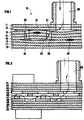
- FIG. 1 illustrates a first embodiment, in which the substrate 10 is formed from a sintered stack of layers 11, 12, ... 18 of dielectric material.
- the internal network of channels is formed by a series of channel segments 21, 22, 23 defined between two adjacent layers (for example layers 12 and 13, or 15 and 16, respectively) by a residual volume formed at the interface of these along a predetermined pattern.
- the interconnections are made by wells 24, 25 formed by removal of material in the layers to be crossed.
- the figure shows the pressure fluid inlet 26 communicating with the internal network of channels.
- This orifice is connected to a primary fluid circuit, generally a closed circuit which recycles the fluid withdrawn from the internal network of the substrate by another orifice (not shown) via a heat exchanger and a pump, according to a classic scheme in itself.
- the cooling fluid can be water, or preferably a suitable inert fluid, such as FLUORINERT (registered trademark of the Company 3M) or GALDEN (registered trademark of the Company MONSANTO), which are fluorinated liquids commonly used for cooling of chassis or radiators of electronic circuits.
- the fluid used can also be a gaseous fluid; the choice is in fact conditioned by the quantity of calories released and by the capacity of the heat exchanger to evacuate the calories taken up in situ.
- the pump and the heat exchanger can be common to the whole apparatus and supply a plurality of substrates designed on the same principle; this centralization, which was not possible with radiators of conventional types (necessarily individual), provides a considerable gain in volume and weight for equipment grouping together a large number of circuits distributed on separate substrates.
- the fluid circulation network can be optimized according to the circuit that is intended to support the substrate: once the hot spots are located (for example by infrared thermography), we seek to reduce the thickness of alumina to be crossed by the calories between the hot spot and the nearest channel ensuring the primary heat exchange, that is to say the absorption of calories in situ.
- high-power circuits that can operate at high ambient temperatures: a maximum operating temperature of 80-85 ° C and a maximum junction temperature of 110-120 ° C indeed limit the maximum temperature difference at around 30 ° .
- Such performances can be achieved, in the range of powers and the format indicated above, thanks to the structure of the invention.
- channels having a maximum thickness of 20 ⁇ m (typically 12-15 gm) and having a width of the order of 1 to 1.5 mm.
- the total thickness of the substrate is of the order of 1 to 1.5 mm, and the use of the particular type of alumina mentioned above makes it possible to circulate the raw fluid directly on the alumina, the latter having practically no porosity ( porosity always less than 1 ⁇ m).
- FIG. 2 illustrates a second embodiment, in which the channel segments are no longer defined at the interface of two adjacent layers, but by removing material in certain layers of the stack, according to a predetermined pattern: in the figure 2, for example, the layers designated 45 to 48 have been perforated in the manner illustrated in FIGS. 3a to 3d, respectively; in FIGS. 3b to 3d, the dotted line shows the pattern of the immediately lower layer, so as to show more clearly the regions through which the fluid can pass from one layer level to the next.
- each of the layers thus perforated can vary between 50 and 250 ⁇ m. If it is expected that there is always a surface common to at least two layers, the passage thickness can thus be 0.1 to 0.5 mm, for a width of the order of 1 mm to 2 mm .
Landscapes
- Engineering & Computer Science (AREA)
- Microelectronics & Electronic Packaging (AREA)
- Cooling Or The Like Of Semiconductors Or Solid State Devices (AREA)
- Production Of Multi-Layered Print Wiring Board (AREA)
- Compositions Of Oxide Ceramics (AREA)
Description
- La présente invention concerne les substrats monolithiques pour composants électroniques de puissance; ces substrats sont formés d'un empilement fritté de couches de matériau diélectrique, généralement une céramique, ou une alumine dans les applications hyperfréquences.
- De tels substrats sont utilisables aussi bien pour supporter des puces semi-conductrices à forte densité (ils sont alors connus sous le nom de "chip carrier"), ou comme substrats destinés à la réalisation de circuits hybrides, selon une technologie classique en elle-même. Dans l'un ou l'autre cas, ces substrats sont souvent des substrats d'interconnexion, c'est-à-dire qu'ils comportent des liaisons conductrices intégrées (enterrées dans le substrat ou formées à sa surface) qui seront par la suite reliées aux bornes du composant. Ces interconnexions sont souvent réparties sur plusieurs couches, des interconnexions de couche à couche et avec la surface du substrat étant incorporées selon un schéma préétabli.
- En raison de la forte densité de composants, ou lorsqu'on souhaite utiliser des composants de puissance (amplificateurs en technologie hybride, par exemple), il devient nécessaire d'absorber et de dissiper un nombre important de calories dégagées par les composants. A titre d'exemple, il est courant d'avoir à dissiper une puissance de l'ordre de 35 watts par un substrat de dimensions normalisées 152,4 x 86,36 mm.
- A cet effet, on choisit généralement pour le substrat un matériau bon conducteur de la chaleur, tel que l'alumine qui présent, en outre, d'excellentes propriétés diélectriques et mécaniques. Ce choix est important surtout lorsque des courants intenses parcourent les interconnexions enterrées, pour drainer les calories depuis le coeur du substrat vers sa surface.
- Pour dissiper les calories ainsi drainées, une première méthode consiste à utiliser des radiateurs métalliques collés au dos du substrat, la chaleur étant évacuée par conduction à travers la masse de ce radiateur, puis par convection naturelle ou forcée vers l'atmosphère ambiante.
- Une autre technique, qui peut être utilisée en combinaison avec la précédente, consiste à prévoir au coeur du substrat des métallisations faisant office de drains thermiques et débouchant sur une face du substrat par des plots qui seront ensuite soudés à un châssis métallique, par exemple en cuivre ou en duralumin.
- Ces deux techniques ont cependant l'inconvénient d'occuper une face entière du substrat qui n'est donc plus disponible pour le report de composants, de nécessiter des masses métalliques importantes pour évacuer les calories par conduction puis convection, et enfin de limiter, pour cette raison, les possibilités de dispositions physiques du substrat et des composants à l'intérieur de l'appareillage.
- En tout état de cause, la possibilité d'absorber in situ les calories dégagées est limitée du fait de l'interposition d'un organe intermédiaire, drain thermique ou radiateur.
- L'invention propose une nouvelle structure de substrat permettant de remédier à ces inconvénients.
- Le substrat de l'invention comporte à cet effet un réseau interne de canaux pour la circulation d'un fluide de refroidissement, ce réseau étant un réseau fermé débouchant en surface du substrat par deux orifices permettant respectivement l'admission du fluide sous pression dans le réseau interne de canaux et son prélèvement hors de ce réseau.
- De préférence, le réseau est formé de segments de canaux répartis sur plusieurs niveaux, ces segments étant interconnectés d'un niveau au suivant.
- De préférence, l'interconnexion de canaux est réalisée par des puits formés par enlèvement de matière dans les couches à traverser.
- En variante ou en complément, l'interconnexion des canaux peut également être réalisée par des régions en regard des segments de canaux appartenant à deux couches adjacentes.
- Dans un premier mode de réalisation, les canaux sont définis entre deux couches adjacentes par un volume résiduel formé à l'interface de celles-ci le long d'un motif prédéterminé.
- Dans un second mode de réalisation, les canaux sont définis par enlèvement de matière dans certaines couches de l'empilement selon un motif prédéterminé.
- L'invention concerne également un procédé de fabrication du substrat selon le premier mode de réalisation précité, dans lequel le volume résiduel est obtenu par dépôt d'une encre évanescente selon le motif prédéterminé sur au moins l'une des feuilles de matériau diélectrique cru avant empilement, cette encre évanescente étant une encre dépourvue de pigment minéral, propre à empêcher au moment de la cuisson le co-frittage des deux couches adjacentes le long dudit motif.
- D'autres caractéristiques et avantages de l'invention apparaîtront plus clairement à la lecture de la description détaillée qui va suivre, faite en référence aux dessins annexés, sur lesquels :
- . la figure 1 est une vue en coupe d'un substrat selon le premier mode de réalisation précité,
- . la figure 2 est homologue de la figure 1, pour le second mode de réalisation précité,
- . les figures 3a à 3d montrent le dessin des ouvertures poinçonnées dans chacune des couches du substrat pour former le réseau de circulation de fluide du second mode de réalisation précité.
- On notera, tout d'abord, que, dans les descriptions qui vont suivre, le réseau de canaux pour la circulation du fluide de refroidissement est intégré au substrat de façon indissociable, les niveaux d'interconnexions électriques et les niveaux d'interconnexions des canaux étant imbriqués. L'invention s'applique cependant également à des substrats dans lesquels le réseau des interconnexions électriques et le réseau des canaux sont deux réseaux étagés, non imbriqués : tel est en particulier le cas lorsque le substrat final est réalisé à partir de deux substrats superposés et solidarisés en un seul élément monolithique (par frittage, collage ...) l'un des substrats de départ étant un substrat d'interconnexion électrique classique, et l'autre substrat de départ étant un substrat spécifique de refroidissement accolé au précédent.
- D'autre part, le matériau préférentiel utilisé pour ces substrats est l'alumine, en raison de ses excellentes propriétés thermiques (très bon conducteur), diélectriques (permettant un emploi en hyperfréquences) et mécaniques. Une composition préférentielle est celle décrite en détail dans la demande de brevet français n° 83-19689 du 8 décembre 1983, au nom de la Demanderesse, intitulée "Substrat d'interconnexion en alumine pour composant électronique": cette composition comprend 92 à 98% d'lI2Os (de préférence 96%), le restant étant constitué de titanate de magnésie dont la formule est comprise entre (Ti02, 0,5 MgO) et (Ti02, 6 MgO), de préférence (Ti02, MgO), les motifs conducteurs étant réalisés en palladium ou en un alliage argent-palladium.
- Cette composition présente l'avantage de conserver toutes les propriétés de l'alumine ultra-pure, en abaissant toutefois la température maximale de cuisson à une valeur de l'ordre de 1400°, cuisson qui au surplus peut être réalisée en atmosphère oxydante.
- Si cette composition est préférentielle, elle n'en est pas pour autant limitative, et d'autres matériaux peuvent être utilisés, tels que l'alumine ultra-pure ou les céramiques de types classiques employées pour ce type de substrat.
- La figure 1 illustre un premier mode de réalisation, dans lequel le substrat 10 est formé d'un empilement fritté de couches 11, 12, ... 18 de matériau diélectrique. Le réseau interne de canaux est formé d'une série de segments de canaux 21, 22, 23 définis entre deux couches adjacentes (par exemple les couches 12 et 13, ou 15 et 16, respectivement) par un volume résiduel formé à l'interface de celles-ci le long d'un motif prédéterminé. Les interconnexions sont réalisées par des puits 24, 25 formés par enlèvement de matière dans les couches à traverser. Sur la figure a été représenté l'orifice d'admission de fluide sous pression 26 communiquant avec le réseau interne de canaux.
- Cet orifice est relié à un circuit primaire de fluide, généralement un circuit fermé qui recycle le fluide prélevé hors du réseau interne du substrat par un autre orifice (non représenté) par l'intermédiaire d'un échangeur thermique et d'une pompe, selon un schéma classique en lui-même. Le fluide de refroidissement peut être l'eau, ou de préférence un fluide inerte approprié, tel que le FLUORINERT (marque déposée de la Société 3M) ou le GALDEN (marque déposée de la Société MONSANTO), qui sont des liquides fluorés couramment utilisés pour le refroidissement des châssis ou des radiateurs de circuits électroniques.
- Le fluide utilisé peut être également un fluide gazeux; le choix est en fait conditionné par la quantité de calories dégagées et par la capacité de l'échangeur thermique à évacuer les calories prélevées in situ.
- La pompe et l'échangeur thermique peuvent être communs à l'ensemble de l'appareillage et alimenter une pluralité de substrats conçus sur le même principe; cette centralisation, qui n'était pas possible avec les radiateurs de types classiques (nécessairement individuels), assure un gain de volume et de poids considérable pour les appareillages regroupant un nombre élevé de circuits répartis sur des substrats distincts.
- Le réseau de circulation de fluide peut être optimisé en fonction du circuit qu'est destiné à supporter le substrat: une fois les points chauds localisés (par exemple par thermographie infrarouge), on cherche à réduire l'épaisseur d'alumine à traverser par les calories entre le point chaud et le canal le plus proche assurant l'échange thermique primaire, c'est-à-dire l'absorption des calories in situ. De la sorte, il est possible de concevoir des circuits de forte puissance pouvant fonctionner à des températures ambiantes élevées: une température maximale de fonctionnement de 80-85°C et une température maximale de jonction de 110-120°C limitent en effet l'écart maximal de température à 30° environ. De telles performances peuvent être atteintes, dans la gamme de puissances et le format indiqués plus haut, grâce à la structure de l'invention.
- Pour réaliser le substrat de la figure 1, le procédé comprend les étapes suivantes:
- -Dépôt sur un certain nombre de couches d'une pâte évanescente (c'est-à-dire une pâte qui disparaîtra totalement lors de la cuisson, donc une encre sans pigment minéral), selon un motif correspondant aux différents segments de canaux à former au niveau correspondant.
- La substance évanescente peut être un liant classique, tel qu'un polyvinylbutyral non chargé, dès lors qu'il est adapté au liant de la céramique, c'est-à-dire qu'il ne réagit pas avec celui-ci.
- ·De la même façon, dépôt d'une encre chargée d'un pigment minéral pour former la réseau d'interconnexions électriques (ces interconnexions sont désignées 31 et 32, par exemple, sur la figure 1).
- 'Perçage des trous d'interconnexions de couche à couche et d'un couche à la surface : il peut s'agir soit d'interconnecter les segments de canaux du réseau de refroidissement (les trous ne sont alors pas métallisés), soit d'interconnecter les pistes conductrices (les trous sont alors métallisés, de façon classique).
- 'Empilement des différentes couche
- -Empilement et compression des différentes couches.
- -Cuisson et frittage du bloc ainsi obtenu: la sur- épaisseur formée à l'endroit où la pâte évanescente a été déposée va empêcher le frittage des deux couches adjacentes; lors de la cuisson, cette pâte va peu à peu disparaître, laissant subsister un volume résiduel à l'interface des deux couches; ce sont ces volumes résiduels qui constitueront ensemble les segments de canaux du réseau de refroidissement.
- Il est possible de réaliser par cette méthode des canaux ayant une épaisseur maximale de 20 µm (typiquement 12-15 gm) et ayant une largeur de l'ordre de 1 à 1,5 mm. L'épaisseur totale du substrat est de l'ordre de 1 à 1,5 mm, et l'utilisation du type particulier d'alumine cité plus haut permet de faire circuler directement le fluide a cru sur l'alumine, celle-ci n'ayant pratiquement pas de porosité (porosité toujours inférieure à 1 µm).
- La figure 2 illustre un second mode de réalisation, dans lequel les segments de canaux ne sont plus définis à l'interface de deux couches adjacentes, mais par enlèvement de matière dans certaines couches de l'empilement, selon un motif prédéterminé: sur la figure 2, on a par exemple perforé les couches désignées 45 à 48 de la manière illustrée figures 3a à 3d, respectivement; sur les figures 3b à 3d, on a illustrée en tireté le motif de la couche immédiatement inférieure, de manière à faire apparaître plus clairement les régions par lesquelles le fluide peut passer d'un niveau de couche au suivant.
- Si l'on considère la figure 3c, on peut observer que deux niveaux de couches pourvus de motifs appropriés sont suffisants pour assurer la circulation du fluide; on préfère cependant ajouter les motifs des couches 45 et 48 pour faciliter la circulation du fluide aux endroits où pourrait se créer une perte de charge.
- L'épaisseur de chacune des couches ainsi perforées peut varier entre 50 et 250 !lm. Si l'on prévoit qu'il existe toujours une surface commune à au moins deux couches, l'épaisseur de passage peut ainsi être de 0,1 à 0,5 mm, pour une largeur de l'ordre de 1 mm à 2 mm.
Claims (7)
Applications Claiming Priority (2)
| Application Number | Priority Date | Filing Date | Title |
|---|---|---|---|
| FR8502749A FR2578099B1 (fr) | 1985-02-26 | 1985-02-26 | Substrat monolithique pour composant electronique de puissance, et procede pour sa fabrication |
| FR8502749 | 1985-02-26 |
Publications (2)
| Publication Number | Publication Date |
|---|---|
| EP0194216A1 EP0194216A1 (fr) | 1986-09-10 |
| EP0194216B1 true EP0194216B1 (fr) | 1989-01-11 |
Family
ID=9316624
Family Applications (1)
| Application Number | Title | Priority Date | Filing Date |
|---|---|---|---|
| EP86420059A Expired EP0194216B1 (fr) | 1985-02-26 | 1986-02-24 | Substrat monolithique pour composant électronique de puissance, et procédé pour sa fabrication |
Country Status (5)
| Country | Link |
|---|---|
| US (2) | US4814030A (fr) |
| EP (1) | EP0194216B1 (fr) |
| JP (1) | JPH063829B2 (fr) |
| DE (1) | DE3661787D1 (fr) |
| FR (1) | FR2578099B1 (fr) |
Families Citing this family (48)
| Publication number | Priority date | Publication date | Assignee | Title |
|---|---|---|---|---|
| US4734315A (en) * | 1985-06-05 | 1988-03-29 | Joyce Florence Space-Bate | Low power circuitry components |
| JPH0746714B2 (ja) * | 1986-09-04 | 1995-05-17 | 日本電信電話株式会社 | 集積回路パツケ−ジ |
| US5077601A (en) * | 1988-09-09 | 1991-12-31 | Hitachi, Ltd. | Cooling system for cooling an electronic device and heat radiation fin for use in the cooling system |
| DE69017095T2 (de) * | 1989-05-19 | 1995-06-14 | Fujitsu Ltd | Anordnung von Strahlaustastungsblenden, Verfahren zur Herstellung derselben, Gerät und Verfahren zur Belichtung von mit einem Strahl geladenen Teilchen. |
| JPH03257953A (ja) * | 1990-03-08 | 1991-11-18 | Nobuo Mikoshiba | 半導体素子 |
| US5239200A (en) * | 1991-08-21 | 1993-08-24 | International Business Machines Corporation | Apparatus for cooling integrated circuit chips |
| IT1252950B (it) * | 1991-09-30 | 1995-07-06 | Gisulfo Baccini | Procedimento di bloccaggio fogli per circuiti green-tape |
| US5177667A (en) * | 1991-10-25 | 1993-01-05 | International Business Machines Corporation | Thermal conduction module with integral impingement cooling |
| US5199165A (en) * | 1991-12-13 | 1993-04-06 | Hewlett-Packard Company | Heat pipe-electrical interconnect integration method for chip modules |
| FR2701554B1 (fr) * | 1993-02-12 | 1995-05-12 | Transcal | Echangeur de chaleur pour composants électroniques et appareillages électro-techniques. |
| JPH07142822A (ja) * | 1993-09-20 | 1995-06-02 | Fujitsu Ltd | 回路基板及びその製造方法 |
| JP3094780B2 (ja) * | 1994-04-05 | 2000-10-03 | 株式会社日立製作所 | 電子装置 |
| US5601673A (en) * | 1995-01-03 | 1997-02-11 | Ferro Corporation | Method of making ceramic article with cavity using LTCC tape |
| US5577657A (en) * | 1995-09-01 | 1996-11-26 | Ford Motor Company | Method of improved oven reflow soldering |
| DE19710716C2 (de) * | 1997-03-14 | 2001-05-10 | Fraunhofer Ges Forschung | Vorrichtung zum Kühlen von elektronischen Bauelementen |
| DE19710783C2 (de) * | 1997-03-17 | 2003-08-21 | Curamik Electronics Gmbh | Kühler zur Verwendung als Wärmesenke für elektrische Bauelemente oder Schaltkreise |
| DE19733455B4 (de) * | 1997-08-02 | 2012-03-29 | Curamik Electronics Gmbh | Wärmetauscheranordnung sowie Kühlsystem mit wenigstens einer derartigen Wärmetauscheranordnung |
| DE19925510A1 (de) * | 1999-06-04 | 2000-12-14 | Schulz Harder Juergen | Kühler zur Verwendung als Wärmesenke für elektrische oder elektronische Komponenten |
| US6242075B1 (en) | 1998-11-20 | 2001-06-05 | Hewlett-Packard Company | Planar multilayer ceramic structures with near surface channels |
| CA2380093A1 (fr) * | 1999-07-27 | 2001-02-01 | North Carolina State University | Film a motifs detachable entre deux surfaces laminees |
| US6473963B1 (en) * | 2000-09-06 | 2002-11-05 | Visteon Global Tech., Inc. | Method of making electrical circuit board |
| JP2002162187A (ja) * | 2000-11-24 | 2002-06-07 | Denso Corp | 積層冷却器 |
| US20020163781A1 (en) * | 2001-05-01 | 2002-11-07 | Ericsson Inc. | Integrated cooling of a printed circuit board structure |
| US6665185B1 (en) * | 2002-10-09 | 2003-12-16 | Ltx Corporation | Apparatus and method for embedded fluid cooling in printed circuit boards |
| US20060016551A1 (en) * | 2004-07-23 | 2006-01-26 | Christensen Donald J | Phenolic lamination process for hot gas components |
| ATE513312T1 (de) † | 2004-12-20 | 2011-07-15 | Iq Evolution Gmbh | Mikrokühlkörper |
| JP4721412B2 (ja) * | 2005-06-28 | 2011-07-13 | 本田技研工業株式会社 | 冷却器およびその製造方法 |
| TW200735308A (en) * | 2005-12-23 | 2007-09-16 | Koninkl Philips Electronics Nv | On-chip interconnect-stack cooling using sacrificial interconnect segments |
| JP2007184479A (ja) * | 2006-01-10 | 2007-07-19 | Toyota Central Res & Dev Lab Inc | 冷却器と、その冷却器上に半導体素子が実装されている半導体装置 |
| WO2007124776A1 (fr) * | 2006-05-03 | 2007-11-08 | Iq Evolution Gmbh | Corps micro-réfrigérant |
| EP2565920A4 (fr) * | 2010-04-28 | 2016-12-21 | Toyota Jidoshokki Kk | Dispositif de dissipation de chaleur et dispositif à semiconducteur |
| US9448014B2 (en) | 2011-10-28 | 2016-09-20 | Kyocera Corporation | Channel member, and heat exchanger, semiconductor unit, and semiconductor manufacturing apparatus including the same |
| DE102012106244B4 (de) * | 2012-07-11 | 2020-02-20 | Rogers Germany Gmbh | Metall-Keramik-Substrat |
| EP2876678A4 (fr) * | 2012-07-18 | 2016-04-13 | Toyota Jidoshokki Kk | Dispositif de dissipation de chaleur et dispositif semi-conducteur |
| JP6138603B2 (ja) * | 2013-06-24 | 2017-05-31 | 新光電気工業株式会社 | 冷却装置、冷却装置の製造方法及び半導体装置 |
| DE102013109246B4 (de) * | 2013-08-27 | 2019-01-31 | Rogers Germany Gmbh | Kühlanordnung und Anordnung damit |
| US9468131B2 (en) * | 2014-04-16 | 2016-10-11 | Raytheon Company | Monolithic multi-module electronics chassis with multi-planar embedded fluid cooling channels |
| WO2016017697A1 (fr) * | 2014-07-29 | 2016-02-04 | 京セラ株式会社 | Échangeur de chaleur |
| CN107924897B (zh) * | 2015-09-18 | 2020-10-23 | 株式会社T.Rad | 层叠芯体型散热器 |
| DE102015118146B4 (de) * | 2015-10-23 | 2017-06-08 | Schweizer Electronic Ag | Kühlmittelanschlusselement und Leiterplatte mit Kühlkanal |
| CN107613652A (zh) * | 2017-09-20 | 2018-01-19 | 四川海英电子科技有限公司 | 高密度互联印刷电路板的制造方法 |
| CN107613653A (zh) * | 2017-09-20 | 2018-01-19 | 四川海英电子科技有限公司 | 高多阶hdi印刷电路板的制作方法 |
| CN111418055B (zh) * | 2017-11-28 | 2024-03-12 | 京瓷株式会社 | 电子元件安装用基板、电子装置以及电子模块 |
| US11848177B2 (en) | 2018-02-23 | 2023-12-19 | Lam Research Corporation | Multi-plate electrostatic chucks with ceramic baseplates |
| US11133211B2 (en) * | 2018-08-22 | 2021-09-28 | Lam Research Corporation | Ceramic baseplate with channels having non-square corners |
| FR3091141B1 (fr) * | 2018-12-21 | 2021-06-25 | Valeo Siemens Eautomotive France Sas | Ensemble électrique d’une barre de connexion électrique et d’un module de refroidissement |
| JP2022520784A (ja) | 2019-02-12 | 2022-04-01 | ラム リサーチ コーポレーション | セラミックモノリシック本体を備えた静電チャック |
| WO2021241643A1 (fr) * | 2020-05-29 | 2021-12-02 | 株式会社巴川製紙所 | Unité de réglage de température |
Family Cites Families (9)
| Publication number | Priority date | Publication date | Assignee | Title |
|---|---|---|---|---|
| US3361195A (en) * | 1966-09-23 | 1968-01-02 | Westinghouse Electric Corp | Heat sink member for a semiconductor device |
| US3852877A (en) * | 1969-08-06 | 1974-12-10 | Ibm | Multilayer circuits |
| US4026746A (en) * | 1976-09-13 | 1977-05-31 | Caterpillar Tractor Co. | Method of manufacturing an open-celled ceramic article |
| JPS542209A (en) * | 1977-06-09 | 1979-01-09 | Nippon Kokan Kk <Nkk> | Dehumidifying method for blast to blast furnace |
| DE3133485A1 (de) * | 1980-09-15 | 1982-05-06 | Peter 2563 Ipsach Herren | Fluessigkeitsgekuehlte elektrische baugruppe |
| US4488920A (en) * | 1982-05-18 | 1984-12-18 | Williams International Corporation | Process of making a ceramic heat exchanger element |
| DE3329325A1 (de) * | 1982-09-03 | 1984-03-08 | Peter 2563 Ipsach Herren | Kuehlkoerper zur fluessigkeitskuehlung wenigstens eines elektrischen leistungselementes |
| JPS59202654A (ja) * | 1983-05-02 | 1984-11-16 | Nippon Telegr & Teleph Corp <Ntt> | 集積回路パツケ−ジ |
| DE3435569A1 (de) * | 1984-09-27 | 1986-04-10 | Siemens AG, 1000 Berlin und 8000 München | Verfahren zur herstellung einer array-ultraschall-antenne |
-
1985
- 1985-02-26 FR FR8502749A patent/FR2578099B1/fr not_active Expired
-
1986
- 1986-02-24 DE DE8686420059T patent/DE3661787D1/de not_active Expired
- 1986-02-24 JP JP61038959A patent/JPH063829B2/ja not_active Expired - Lifetime
- 1986-02-24 EP EP86420059A patent/EP0194216B1/fr not_active Expired
-
1987
- 1987-11-09 US US07/124,544 patent/US4814030A/en not_active Expired - Fee Related
-
1988
- 1988-03-09 US US07/169,125 patent/US4859520A/en not_active Expired - Fee Related
Also Published As
| Publication number | Publication date |
|---|---|
| DE3661787D1 (en) | 1989-02-16 |
| FR2578099B1 (fr) | 1987-12-04 |
| JPH063829B2 (ja) | 1994-01-12 |
| EP0194216A1 (fr) | 1986-09-10 |
| US4814030A (en) | 1989-03-21 |
| FR2578099A1 (fr) | 1986-08-29 |
| US4859520A (en) | 1989-08-22 |
| JPS61196558A (ja) | 1986-08-30 |
Similar Documents
| Publication | Publication Date | Title |
|---|---|---|
| EP0194216A1 (fr) | Substrat monolithique pour composant électronique de puissance, et procédé pour sa fabrication | |
| EP0145599B1 (fr) | Substrat d'interconnexion en alumine pour composant électronique, et procédé pour sa fabrication | |
| EP1636130B1 (fr) | Circuit integre sur puce de hautes performances | |
| EP0133125B1 (fr) | Boîtier de composant électronique muni d'un condensateur | |
| US20060027934A1 (en) | Silicon chip carrier with conductive through-vias and method for fabricating same | |
| FR2606206A1 (fr) | Condensateur de decouplage pour module a reseau d'ergots en grille | |
| EP0920036A1 (fr) | Transformateur en circuit intégré | |
| EP0325068B1 (fr) | Structure microélectronique hybride modulaire à haute densité d'intégration | |
| EP0296997A1 (fr) | Structure de transistors MOS de puissance | |
| FR2760593A1 (fr) | Ensemble electrique a forte dissipation de chaleur | |
| WO2003019668A1 (fr) | Capteur d'image couleur a colorimetrie amelioree et procede de fabrication | |
| EP0149932B1 (fr) | Support pour composant rapide, notamment composant hyperfréquence, à éléments de découplage incorpores | |
| FR2741197A1 (fr) | Procede de fabrication d'un module de conversion thermoelectrique | |
| FR2767223A1 (fr) | Procede d'interconnexion a travers un materiau semi-conducteur, et dispositif obtenu | |
| US20190159294A1 (en) | Integrated heater and method of manufacture | |
| CA2357317A1 (fr) | Substrat pour circuit electronique et module electronique utilisant un tel substrat | |
| EP0951067B1 (fr) | Circuit intégré avec couche d'arrêt et procédé de fabrication associé | |
| EP0091075B1 (fr) | Procédé d'élaboration de circuits d'interconnexion multicouches | |
| KR20210013106A (ko) | 일체형 히터와 제조 방법 | |
| FR2667443A1 (fr) | Procede de realisation d'un module hybride. | |
| FR2976720A1 (fr) | Procede de connexion electrique entre des elements d'une structure integree tridimensionnelle, et dispositif correspondant | |
| FR2819100A1 (fr) | Procede d'empilage de circuits integres | |
| FR2864342A1 (fr) | Procede d'interconnexion de composants electroniques sans apport de brasure et dispositif electronique obtenu par un tel procede | |
| WO2000008900A1 (fr) | Carte de circuits imprimes | |
| EP3855483B1 (fr) | Connexions traversant un interposeur utilisant des trous d'interconnexion borgnes |
Legal Events
| Date | Code | Title | Description |
|---|---|---|---|
| PUAI | Public reference made under article 153(3) epc to a published international application that has entered the european phase |
Free format text: ORIGINAL CODE: 0009012 |
|
| AK | Designated contracting states |
Kind code of ref document: A1 Designated state(s): DE FR GB IT NL |
|
| 17P | Request for examination filed |
Effective date: 19860929 |
|
| 17Q | First examination report despatched |
Effective date: 19880322 |
|
| RAP3 | Party data changed (applicant data changed or rights of an application transferred) |
Owner name: XERAM |
|
| GRAA | (expected) grant |
Free format text: ORIGINAL CODE: 0009210 |
|
| AK | Designated contracting states |
Kind code of ref document: B1 Designated state(s): DE FR GB IT NL |
|
| ITF | It: translation for a ep patent filed | ||
| GBT | Gb: translation of ep patent filed (gb section 77(6)(a)/1977) | ||
| REF | Corresponds to: |
Ref document number: 3661787 Country of ref document: DE Date of ref document: 19890216 |
|
| PLBE | No opposition filed within time limit |
Free format text: ORIGINAL CODE: 0009261 |
|
| STAA | Information on the status of an ep patent application or granted ep patent |
Free format text: STATUS: NO OPPOSITION FILED WITHIN TIME LIMIT |
|
| 26N | No opposition filed | ||
| ITTA | It: last paid annual fee | ||
| PGFP | Annual fee paid to national office [announced via postgrant information from national office to epo] |
Ref country code: FR Payment date: 19940110 Year of fee payment: 9 |
|
| PGFP | Annual fee paid to national office [announced via postgrant information from national office to epo] |
Ref country code: GB Payment date: 19940223 Year of fee payment: 9 |
|
| PGFP | Annual fee paid to national office [announced via postgrant information from national office to epo] |
Ref country code: NL Payment date: 19940228 Year of fee payment: 9 |
|
| PGFP | Annual fee paid to national office [announced via postgrant information from national office to epo] |
Ref country code: DE Payment date: 19940428 Year of fee payment: 9 |
|
| PG25 | Lapsed in a contracting state [announced via postgrant information from national office to epo] |
Ref country code: GB Effective date: 19950224 |
|
| PG25 | Lapsed in a contracting state [announced via postgrant information from national office to epo] |
Ref country code: NL Effective date: 19950901 |
|
| GBPC | Gb: european patent ceased through non-payment of renewal fee |
Effective date: 19950224 |
|
| PG25 | Lapsed in a contracting state [announced via postgrant information from national office to epo] |
Ref country code: FR Effective date: 19951031 |
|
| NLV4 | Nl: lapsed or anulled due to non-payment of the annual fee |
Effective date: 19950901 |
|
| PG25 | Lapsed in a contracting state [announced via postgrant information from national office to epo] |
Ref country code: DE Effective date: 19951101 |
|
| REG | Reference to a national code |
Ref country code: FR Ref legal event code: ST |
|
| PG25 | Lapsed in a contracting state [announced via postgrant information from national office to epo] |
Ref country code: IT Free format text: LAPSE BECAUSE OF NON-PAYMENT OF DUE FEES;WARNING: LAPSES OF ITALIAN PATENTS WITH EFFECTIVE DATE BEFORE 2007 MAY HAVE OCCURRED AT ANY TIME BEFORE 2007. THE CORRECT EFFECTIVE DATE MAY BE DIFFERENT FROM THE ONE RECORDED. Effective date: 20050224 |