EP0192233B1 - Molded metallized articles and processes for making the same - Google Patents
Molded metallized articles and processes for making the same Download PDFInfo
- Publication number
- EP0192233B1 EP0192233B1 EP86102055A EP86102055A EP0192233B1 EP 0192233 B1 EP0192233 B1 EP 0192233B1 EP 86102055 A EP86102055 A EP 86102055A EP 86102055 A EP86102055 A EP 86102055A EP 0192233 B1 EP0192233 B1 EP 0192233B1
- Authority
- EP
- European Patent Office
- Prior art keywords
- article
- catalyst
- circuit pattern
- molded
- insulating material
- Prior art date
- Legal status (The legal status is an assumption and is not a legal conclusion. Google has not performed a legal analysis and makes no representation as to the accuracy of the status listed.)
- Expired - Lifetime
Links
Images


Classifications
-
- H—ELECTRICITY
- H05—ELECTRIC TECHNIQUES NOT OTHERWISE PROVIDED FOR
- H05K—PRINTED CIRCUITS; CASINGS OR CONSTRUCTIONAL DETAILS OF ELECTRIC APPARATUS; MANUFACTURE OF ASSEMBLAGES OF ELECTRICAL COMPONENTS
- H05K3/00—Apparatus or processes for manufacturing printed circuits
- H05K3/10—Apparatus or processes for manufacturing printed circuits in which conductive material is applied to the insulating support in such a manner as to form the desired conductive pattern
- H05K3/18—Apparatus or processes for manufacturing printed circuits in which conductive material is applied to the insulating support in such a manner as to form the desired conductive pattern using precipitation techniques to apply the conductive material
- H05K3/181—Apparatus or processes for manufacturing printed circuits in which conductive material is applied to the insulating support in such a manner as to form the desired conductive pattern using precipitation techniques to apply the conductive material by electroless plating
- H05K3/182—Apparatus or processes for manufacturing printed circuits in which conductive material is applied to the insulating support in such a manner as to form the desired conductive pattern using precipitation techniques to apply the conductive material by electroless plating characterised by the patterning method
-
- C—CHEMISTRY; METALLURGY
- C23—COATING METALLIC MATERIAL; COATING MATERIAL WITH METALLIC MATERIAL; CHEMICAL SURFACE TREATMENT; DIFFUSION TREATMENT OF METALLIC MATERIAL; COATING BY VACUUM EVAPORATION, BY SPUTTERING, BY ION IMPLANTATION OR BY CHEMICAL VAPOUR DEPOSITION, IN GENERAL; INHIBITING CORROSION OF METALLIC MATERIAL OR INCRUSTATION IN GENERAL
- C23C—COATING METALLIC MATERIAL; COATING MATERIAL WITH METALLIC MATERIAL; SURFACE TREATMENT OF METALLIC MATERIAL BY DIFFUSION INTO THE SURFACE, BY CHEMICAL CONVERSION OR SUBSTITUTION; COATING BY VACUUM EVAPORATION, BY SPUTTERING, BY ION IMPLANTATION OR BY CHEMICAL VAPOUR DEPOSITION, IN GENERAL
- C23C18/00—Chemical coating by decomposition of either liquid compounds or solutions of the coating forming compounds, without leaving reaction products of surface material in the coating; Contact plating
- C23C18/16—Chemical coating by decomposition of either liquid compounds or solutions of the coating forming compounds, without leaving reaction products of surface material in the coating; Contact plating by reduction or substitution, e.g. electroless plating
- C23C18/1601—Process or apparatus
- C23C18/1603—Process or apparatus coating on selected surface areas
- C23C18/1607—Process or apparatus coating on selected surface areas by direct patterning
- C23C18/1608—Process or apparatus coating on selected surface areas by direct patterning from pretreatment step, i.e. selective pre-treatment
-
- C—CHEMISTRY; METALLURGY
- C23—COATING METALLIC MATERIAL; COATING MATERIAL WITH METALLIC MATERIAL; CHEMICAL SURFACE TREATMENT; DIFFUSION TREATMENT OF METALLIC MATERIAL; COATING BY VACUUM EVAPORATION, BY SPUTTERING, BY ION IMPLANTATION OR BY CHEMICAL VAPOUR DEPOSITION, IN GENERAL; INHIBITING CORROSION OF METALLIC MATERIAL OR INCRUSTATION IN GENERAL
- C23C—COATING METALLIC MATERIAL; COATING MATERIAL WITH METALLIC MATERIAL; SURFACE TREATMENT OF METALLIC MATERIAL BY DIFFUSION INTO THE SURFACE, BY CHEMICAL CONVERSION OR SUBSTITUTION; COATING BY VACUUM EVAPORATION, BY SPUTTERING, BY ION IMPLANTATION OR BY CHEMICAL VAPOUR DEPOSITION, IN GENERAL
- C23C18/00—Chemical coating by decomposition of either liquid compounds or solutions of the coating forming compounds, without leaving reaction products of surface material in the coating; Contact plating
- C23C18/16—Chemical coating by decomposition of either liquid compounds or solutions of the coating forming compounds, without leaving reaction products of surface material in the coating; Contact plating by reduction or substitution, e.g. electroless plating
- C23C18/1601—Process or apparatus
- C23C18/1603—Process or apparatus coating on selected surface areas
- C23C18/1607—Process or apparatus coating on selected surface areas by direct patterning
- C23C18/1612—Process or apparatus coating on selected surface areas by direct patterning through irradiation means
-
- C—CHEMISTRY; METALLURGY
- C23—COATING METALLIC MATERIAL; COATING MATERIAL WITH METALLIC MATERIAL; CHEMICAL SURFACE TREATMENT; DIFFUSION TREATMENT OF METALLIC MATERIAL; COATING BY VACUUM EVAPORATION, BY SPUTTERING, BY ION IMPLANTATION OR BY CHEMICAL VAPOUR DEPOSITION, IN GENERAL; INHIBITING CORROSION OF METALLIC MATERIAL OR INCRUSTATION IN GENERAL
- C23C—COATING METALLIC MATERIAL; COATING MATERIAL WITH METALLIC MATERIAL; SURFACE TREATMENT OF METALLIC MATERIAL BY DIFFUSION INTO THE SURFACE, BY CHEMICAL CONVERSION OR SUBSTITUTION; COATING BY VACUUM EVAPORATION, BY SPUTTERING, BY ION IMPLANTATION OR BY CHEMICAL VAPOUR DEPOSITION, IN GENERAL
- C23C18/00—Chemical coating by decomposition of either liquid compounds or solutions of the coating forming compounds, without leaving reaction products of surface material in the coating; Contact plating
- C23C18/16—Chemical coating by decomposition of either liquid compounds or solutions of the coating forming compounds, without leaving reaction products of surface material in the coating; Contact plating by reduction or substitution, e.g. electroless plating
- C23C18/1601—Process or apparatus
- C23C18/1633—Process of electroless plating
- C23C18/1635—Composition of the substrate
- C23C18/1639—Substrates other than metallic, e.g. inorganic or organic or non-conductive
- C23C18/1641—Organic substrates, e.g. resin, plastic
-
- C—CHEMISTRY; METALLURGY
- C23—COATING METALLIC MATERIAL; COATING MATERIAL WITH METALLIC MATERIAL; CHEMICAL SURFACE TREATMENT; DIFFUSION TREATMENT OF METALLIC MATERIAL; COATING BY VACUUM EVAPORATION, BY SPUTTERING, BY ION IMPLANTATION OR BY CHEMICAL VAPOUR DEPOSITION, IN GENERAL; INHIBITING CORROSION OF METALLIC MATERIAL OR INCRUSTATION IN GENERAL
- C23C—COATING METALLIC MATERIAL; COATING MATERIAL WITH METALLIC MATERIAL; SURFACE TREATMENT OF METALLIC MATERIAL BY DIFFUSION INTO THE SURFACE, BY CHEMICAL CONVERSION OR SUBSTITUTION; COATING BY VACUUM EVAPORATION, BY SPUTTERING, BY ION IMPLANTATION OR BY CHEMICAL VAPOUR DEPOSITION, IN GENERAL
- C23C18/00—Chemical coating by decomposition of either liquid compounds or solutions of the coating forming compounds, without leaving reaction products of surface material in the coating; Contact plating
- C23C18/16—Chemical coating by decomposition of either liquid compounds or solutions of the coating forming compounds, without leaving reaction products of surface material in the coating; Contact plating by reduction or substitution, e.g. electroless plating
- C23C18/18—Pretreatment of the material to be coated
- C23C18/20—Pretreatment of the material to be coated of organic surfaces, e.g. resins
- C23C18/2006—Pretreatment of the material to be coated of organic surfaces, e.g. resins by other methods than those of C23C18/22 - C23C18/30
- C23C18/2026—Pretreatment of the material to be coated of organic surfaces, e.g. resins by other methods than those of C23C18/22 - C23C18/30 by radiant energy
- C23C18/204—Radiation, e.g. UV, laser
-
- C—CHEMISTRY; METALLURGY
- C23—COATING METALLIC MATERIAL; COATING MATERIAL WITH METALLIC MATERIAL; CHEMICAL SURFACE TREATMENT; DIFFUSION TREATMENT OF METALLIC MATERIAL; COATING BY VACUUM EVAPORATION, BY SPUTTERING, BY ION IMPLANTATION OR BY CHEMICAL VAPOUR DEPOSITION, IN GENERAL; INHIBITING CORROSION OF METALLIC MATERIAL OR INCRUSTATION IN GENERAL
- C23C—COATING METALLIC MATERIAL; COATING MATERIAL WITH METALLIC MATERIAL; SURFACE TREATMENT OF METALLIC MATERIAL BY DIFFUSION INTO THE SURFACE, BY CHEMICAL CONVERSION OR SUBSTITUTION; COATING BY VACUUM EVAPORATION, BY SPUTTERING, BY ION IMPLANTATION OR BY CHEMICAL VAPOUR DEPOSITION, IN GENERAL
- C23C18/00—Chemical coating by decomposition of either liquid compounds or solutions of the coating forming compounds, without leaving reaction products of surface material in the coating; Contact plating
- C23C18/16—Chemical coating by decomposition of either liquid compounds or solutions of the coating forming compounds, without leaving reaction products of surface material in the coating; Contact plating by reduction or substitution, e.g. electroless plating
- C23C18/18—Pretreatment of the material to be coated
- C23C18/20—Pretreatment of the material to be coated of organic surfaces, e.g. resins
- C23C18/2006—Pretreatment of the material to be coated of organic surfaces, e.g. resins by other methods than those of C23C18/22 - C23C18/30
- C23C18/2046—Pretreatment of the material to be coated of organic surfaces, e.g. resins by other methods than those of C23C18/22 - C23C18/30 by chemical pretreatment
- C23C18/2073—Multistep pretreatment
- C23C18/208—Multistep pretreatment with use of metal first
-
- C—CHEMISTRY; METALLURGY
- C23—COATING METALLIC MATERIAL; COATING MATERIAL WITH METALLIC MATERIAL; CHEMICAL SURFACE TREATMENT; DIFFUSION TREATMENT OF METALLIC MATERIAL; COATING BY VACUUM EVAPORATION, BY SPUTTERING, BY ION IMPLANTATION OR BY CHEMICAL VAPOUR DEPOSITION, IN GENERAL; INHIBITING CORROSION OF METALLIC MATERIAL OR INCRUSTATION IN GENERAL
- C23C—COATING METALLIC MATERIAL; COATING MATERIAL WITH METALLIC MATERIAL; SURFACE TREATMENT OF METALLIC MATERIAL BY DIFFUSION INTO THE SURFACE, BY CHEMICAL CONVERSION OR SUBSTITUTION; COATING BY VACUUM EVAPORATION, BY SPUTTERING, BY ION IMPLANTATION OR BY CHEMICAL VAPOUR DEPOSITION, IN GENERAL
- C23C18/00—Chemical coating by decomposition of either liquid compounds or solutions of the coating forming compounds, without leaving reaction products of surface material in the coating; Contact plating
- C23C18/16—Chemical coating by decomposition of either liquid compounds or solutions of the coating forming compounds, without leaving reaction products of surface material in the coating; Contact plating by reduction or substitution, e.g. electroless plating
- C23C18/18—Pretreatment of the material to be coated
- C23C18/20—Pretreatment of the material to be coated of organic surfaces, e.g. resins
- C23C18/22—Roughening, e.g. by etching
- C23C18/24—Roughening, e.g. by etching using acid aqueous solutions
-
- C—CHEMISTRY; METALLURGY
- C23—COATING METALLIC MATERIAL; COATING MATERIAL WITH METALLIC MATERIAL; CHEMICAL SURFACE TREATMENT; DIFFUSION TREATMENT OF METALLIC MATERIAL; COATING BY VACUUM EVAPORATION, BY SPUTTERING, BY ION IMPLANTATION OR BY CHEMICAL VAPOUR DEPOSITION, IN GENERAL; INHIBITING CORROSION OF METALLIC MATERIAL OR INCRUSTATION IN GENERAL
- C23C—COATING METALLIC MATERIAL; COATING MATERIAL WITH METALLIC MATERIAL; SURFACE TREATMENT OF METALLIC MATERIAL BY DIFFUSION INTO THE SURFACE, BY CHEMICAL CONVERSION OR SUBSTITUTION; COATING BY VACUUM EVAPORATION, BY SPUTTERING, BY ION IMPLANTATION OR BY CHEMICAL VAPOUR DEPOSITION, IN GENERAL
- C23C18/00—Chemical coating by decomposition of either liquid compounds or solutions of the coating forming compounds, without leaving reaction products of surface material in the coating; Contact plating
- C23C18/16—Chemical coating by decomposition of either liquid compounds or solutions of the coating forming compounds, without leaving reaction products of surface material in the coating; Contact plating by reduction or substitution, e.g. electroless plating
- C23C18/18—Pretreatment of the material to be coated
- C23C18/20—Pretreatment of the material to be coated of organic surfaces, e.g. resins
- C23C18/28—Sensitising or activating
- C23C18/30—Activating or accelerating or sensitising with palladium or other noble metal
-
- C—CHEMISTRY; METALLURGY
- C23—COATING METALLIC MATERIAL; COATING MATERIAL WITH METALLIC MATERIAL; CHEMICAL SURFACE TREATMENT; DIFFUSION TREATMENT OF METALLIC MATERIAL; COATING BY VACUUM EVAPORATION, BY SPUTTERING, BY ION IMPLANTATION OR BY CHEMICAL VAPOUR DEPOSITION, IN GENERAL; INHIBITING CORROSION OF METALLIC MATERIAL OR INCRUSTATION IN GENERAL
- C23C—COATING METALLIC MATERIAL; COATING MATERIAL WITH METALLIC MATERIAL; SURFACE TREATMENT OF METALLIC MATERIAL BY DIFFUSION INTO THE SURFACE, BY CHEMICAL CONVERSION OR SUBSTITUTION; COATING BY VACUUM EVAPORATION, BY SPUTTERING, BY ION IMPLANTATION OR BY CHEMICAL VAPOUR DEPOSITION, IN GENERAL
- C23C18/00—Chemical coating by decomposition of either liquid compounds or solutions of the coating forming compounds, without leaving reaction products of surface material in the coating; Contact plating
- C23C18/16—Chemical coating by decomposition of either liquid compounds or solutions of the coating forming compounds, without leaving reaction products of surface material in the coating; Contact plating by reduction or substitution, e.g. electroless plating
- C23C18/31—Coating with metals
- C23C18/38—Coating with copper
-
- H—ELECTRICITY
- H05—ELECTRIC TECHNIQUES NOT OTHERWISE PROVIDED FOR
- H05K—PRINTED CIRCUITS; CASINGS OR CONSTRUCTIONAL DETAILS OF ELECTRIC APPARATUS; MANUFACTURE OF ASSEMBLAGES OF ELECTRICAL COMPONENTS
- H05K3/00—Apparatus or processes for manufacturing printed circuits
- H05K3/0011—Working of insulating substrates or insulating layers
- H05K3/0014—Shaping of the substrate, e.g. by moulding
-
- H—ELECTRICITY
- H05—ELECTRIC TECHNIQUES NOT OTHERWISE PROVIDED FOR
- H05K—PRINTED CIRCUITS; CASINGS OR CONSTRUCTIONAL DETAILS OF ELECTRIC APPARATUS; MANUFACTURE OF ASSEMBLAGES OF ELECTRICAL COMPONENTS
- H05K1/00—Printed circuits
- H05K1/02—Details
- H05K1/0284—Details of three-dimensional rigid printed circuit boards
-
- H—ELECTRICITY
- H05—ELECTRIC TECHNIQUES NOT OTHERWISE PROVIDED FOR
- H05K—PRINTED CIRCUITS; CASINGS OR CONSTRUCTIONAL DETAILS OF ELECTRIC APPARATUS; MANUFACTURE OF ASSEMBLAGES OF ELECTRICAL COMPONENTS
- H05K1/00—Printed circuits
- H05K1/02—Details
- H05K1/03—Use of materials for the substrate
- H05K1/0313—Organic insulating material
- H05K1/0353—Organic insulating material consisting of two or more materials, e.g. two or more polymers, polymer + filler, + reinforcement
- H05K1/0373—Organic insulating material consisting of two or more materials, e.g. two or more polymers, polymer + filler, + reinforcement containing additives, e.g. fillers
-
- H—ELECTRICITY
- H05—ELECTRIC TECHNIQUES NOT OTHERWISE PROVIDED FOR
- H05K—PRINTED CIRCUITS; CASINGS OR CONSTRUCTIONAL DETAILS OF ELECTRIC APPARATUS; MANUFACTURE OF ASSEMBLAGES OF ELECTRICAL COMPONENTS
- H05K2201/00—Indexing scheme relating to printed circuits covered by H05K1/00
- H05K2201/01—Dielectrics
- H05K2201/0104—Properties and characteristics in general
- H05K2201/0129—Thermoplastic polymer, e.g. auto-adhesive layer; Shaping of thermoplastic polymer
-
- H—ELECTRICITY
- H05—ELECTRIC TECHNIQUES NOT OTHERWISE PROVIDED FOR
- H05K—PRINTED CIRCUITS; CASINGS OR CONSTRUCTIONAL DETAILS OF ELECTRIC APPARATUS; MANUFACTURE OF ASSEMBLAGES OF ELECTRICAL COMPONENTS
- H05K2201/00—Indexing scheme relating to printed circuits covered by H05K1/00
- H05K2201/01—Dielectrics
- H05K2201/0183—Dielectric layers
- H05K2201/0187—Dielectric layers with regions of different dielectrics in the same layer, e.g. in a printed capacitor for locally changing the dielectric properties
-
- H—ELECTRICITY
- H05—ELECTRIC TECHNIQUES NOT OTHERWISE PROVIDED FOR
- H05K—PRINTED CIRCUITS; CASINGS OR CONSTRUCTIONAL DETAILS OF ELECTRIC APPARATUS; MANUFACTURE OF ASSEMBLAGES OF ELECTRICAL COMPONENTS
- H05K2201/00—Indexing scheme relating to printed circuits covered by H05K1/00
- H05K2201/02—Fillers; Particles; Fibers; Reinforcement materials
- H05K2201/0203—Fillers and particles
- H05K2201/0206—Materials
- H05K2201/0236—Plating catalyst as filler in insulating material
-
- H—ELECTRICITY
- H05—ELECTRIC TECHNIQUES NOT OTHERWISE PROVIDED FOR
- H05K—PRINTED CIRCUITS; CASINGS OR CONSTRUCTIONAL DETAILS OF ELECTRIC APPARATUS; MANUFACTURE OF ASSEMBLAGES OF ELECTRICAL COMPONENTS
- H05K2201/00—Indexing scheme relating to printed circuits covered by H05K1/00
- H05K2201/09—Shape and layout
- H05K2201/09009—Substrate related
- H05K2201/09118—Moulded substrate
-
- H—ELECTRICITY
- H05—ELECTRIC TECHNIQUES NOT OTHERWISE PROVIDED FOR
- H05K—PRINTED CIRCUITS; CASINGS OR CONSTRUCTIONAL DETAILS OF ELECTRIC APPARATUS; MANUFACTURE OF ASSEMBLAGES OF ELECTRICAL COMPONENTS
- H05K2203/00—Indexing scheme relating to apparatus or processes for manufacturing printed circuits covered by H05K3/00
- H05K2203/14—Related to the order of processing steps
- H05K2203/1476—Same or similar kind of process performed in phases, e.g. coarse patterning followed by fine patterning
Definitions
- This invention relates to molded one-piece articles having selected surface areas suitable for adherent metallization or molded metallized articles and processes for forming the articles. More particularly, this invention relates to molded, one-piece articles comprising an electric circuit pattern and processes for forming the said articles.
- US 3 629 185 there is described a process for forming a metallized article, such as a printed circuit board, having an insulating substrate as a base material.
- the process uses a plastic substrate filled with a powder catalyst which promotes metal deposition in a subsequent electroless metal plating step.
- the process also includes using a direct or reverse printing technique for preparing specific surface areas of the substrate to form the printed circuit for metallization. When high quantity production is needed, the printing step becomes costly.
- US 4 402 135 describes a process for forming printed circuit boards which employs two separate injection molding steps to form a circuit pattern on a support board.
- an electrically insulating plastic material for the substrate is injection molded.
- an electrically conductive plastic material is injection molded.
- the electrically conductive plastic material is electroplated with metal to form electrically conductive paths.
- a disadvantage of this method is that an excessive number of gates are required in the second cavity mold to fill several channels on the upper and lower surfaces, of the support member to provide a circuit pattern with several electrically conductive paths.
- Another disadvantage of this method is that the electrically conductive plastic strips may separate or peel off from the support member due to a lack of rigid connecting structure between the several plastic strips, particularly between the plastic strips on the upper and lower surfaces of the support member.
- the plateable plastics material is not catalytic for metal deposition per se, but is rendered catalytic by exposure of the molded article to a catalyzing solution.
- a further object of this invention is to form a molded article comprising an electric circuit pattern, by forming a first electrically insulating material into a first predetermined shape and by molding a second electrically insulating material into a second predetermined shape which includes interconnecting the second predetermined shape with the first predetermined shape to produce a one-piece article.
- Another object of the invention is to form a molded article comprising an electric circuit pattern by an additive process using a minimum of steps.
- a still further object of the invention is to form a molded article comprising an electric circuit pattern which has an additional integral molded structure.
- a further object of this invention is to mold an article by an alternate two-shot injection molding press.
- the first shot of this alternate process forms a first predetermined shape of the article using a first electrically insulating material selected to avoid metal adherence.
- the second shot of this alternate process forms a second predetermined shape of the article using a second electrically insulating material catalyzed for metal adherence.
- a process for producing a unitary non-conductive article comprising an electric circuit pattern, said process comprising the steps of molding a first insulating material into at least one first predetermined shape, said first material being catalytic for adherent metallization and capable to be catalyst-activated by an adhesion promotion catalyst activation process; molding a second electrically insulating material into at least one second predetermined shape, said second material being non-catalytic for adherent metallization and incapable to be catalyst-activated by the said adhesion promotion catalyst activation process; interconnecting said first and second shape to produce the unitary, one-piece, non-conductive article wherein selected surface areas of said article defined by exposed portions of the said first material are suitable for adherent metallization; exposing the surface of said article to the adhesion promotion catalyst activation process; and forming an adherent metal deposit on said exposed portions of said first insulating material.
- a process for producing a unitary non-conductive article comprising an electric circuit pattern, said process comprising the steps of molding a first insulating material into at least one first predetermined shape, said first material being non-catalytic for adherent metallization and incapable to be catalyst-activated by an adhesion promotion catalyst activation process; molding a second electrically insulating material into at least one second predetermined shape, said second material being catalytic for adherent metallization and capable to be catalyst-activated by the said adhesion promotion catalyst activation process; interconnecting said first and second shape to produce the unitary, one-piece, non-conductive article wherein selected surface areas of said article defined by exposed portions of the said second material are suitable for adherent metallization; exposing the surface of said article to the adhesion promotion catalyst activation process; and forming an adherent metal deposit on said exposed portions of said second material.
- a molded unitary article comprising an electric circuit pattern, said article comprising at least a first predetermined shape comprised of a first electrically insulating material comprising a filler catalyst and capable to be catalyst activated by an adhesion promotion process causing catalyst activation; at least a second predetermined shape comprised of a second electrically insulating material, said material being free of a filler catalyst; said first and said second materials defining first and second patterns on a surface of the molded article, said first pattern being suitable for adherent metallization and said second pattern being resistant to adherent metallization; and a metal layer adhered to said first pattern with the second pattern completely free of metal deposit.
- a method for forming a molded article for adherent metallization such as a printed circuit board, using a two-shot injection molding process.
- the process includes a first step of forming at least one first predetermined shape, such as a circuit pattern for a printed circuit board, by injection molding a first shot of electrically insulating material into a first mold cavity.
- the metal can be copper to form electrically conductive paths on a printed circuit board.
- a second step is to remove the first predetermined shape from the first mold cavity and to insert it into a second mold cavity.
- a third step is to form at least one second predetermined shape of the article, such as a support substrate for a printed circuit board, by injection molding a second shot of electrically insulating material into the second mold cavity.
- the second predetermined shape interconnects with the first predetermined shape to produce a molded one-piece article.
- the electrically insulating material selected for the second shot avoids metal adherence and performs as an electrically insulating material for a printed circuit board.
- the article is then removed from the second mold cavity and processed by an additive process through a minimal series of steps to add metal only on exposed and thus selected surface areas of the first predetermined shape of the first shot injection molding.
- a circuit pattern 30 is formed by a first shot injection molding process in a first mold cavity 32.
- a preferred first electrically insulating material 34 selected for this circuit pattern is polyethersulfone with a catalyst.
- a suitable polyethersulfone is Victrex® 4100 G, one suitable filler catalyst is a palladium catalyst dispersed on a powdered aluminum silicate clay as is disclosed in US Patent 3 600 330 by Examples 6 and 9.
- the catalyst mixed into the first electrically insulating material 34 catalyzes the material for electroless metal deposition in subsequent steps in the process.
- the electrically insulating material 34 can be treated by a minimal series of steps to add metal for forming electrically conductive paths 36 in a printed circuit board.
- Adhesion promotion of insulating materials containing the catalyst activates the material for electroless metal deposition.
- Approximately 20% glass filler can be added to the electrically insulating material 34.
- the metal surfaces formed on the base material are smoother when using polyethersulfone without glass filler.
- circuit pattern 30 Other suitable electrically insulating materials for the circuit pattern 30 are ceramics, thermoset polymers and high temperature thermoplastic materials selected from a group consisting of polysulfone, polyethermimide, polyethersulfone, polyphenylene sulfide and polyetheretherketone.
- the circuit pattern 30 has serveral full surface sections 38 on a first or component side 40.
- the circuit pattern 30 has a web portion 46 for connecting the full surface sections 38 to each other and for spacing the full surface sections 38 relative to each other. The web portion 46 is recessed below the full surface sections 38.
- a second or solder side 48 of the circuit pattern 30 has several full surface sections 50 (only one shown).
- the web portion 46 connects the full surface sections 50 to each other and spaces the full surface sections 50 relative to each other.
- the circuit pattern 30 having the full surface sections 38, the full surface sections 50 and the web portion 46 fabricated by the first shot injection molding process forms a one-piece integral unit.
- a feature of this invention is that the web portion 46 provides a rigid connecting structure between the full surface sections 38 on the component side 40 and the full surface sections 50 on the solder side 48 as well as between the several full surface sections 38 and 50 on each side of the circuit pattern.
- circuit pattern 30 with the web portion 46 can be used as both the circuit pattern and an insulating substrate by selective treatment of the circuit pattern 30 to form electrically conductive paths 36.
- the circuit pattern 30 has been removed from the first mold cavity 32 and inserted into a second mold cavity 52.
- a support structure 54 is formed by a second shot injection molding Process in the second mold cavity 52 and onto the molded circuit pattern 30.
- a preferred second electrically insulating material 56 selected for the support structure 54 is polyethersulfone (Victrex® 200P without catalyst).
- the electrically insulating material 56 may be with glass, mineral or other fillers. It is believed that it is preferable to use reinforcing fillers in this material to provide rigidity to the support structure 54.
- Other suitable materials for the second insulating material include ceramics, thermoset resins, and high temperature thermoplastic materials including polyesters.
- the electrically insulating material 56 of the support structure 54 covers the web portion 46 on the component side 40 and on the solder side 48 of the circuit pattern 30 while leaving the full surface sections 38 and 50 exposed.
- the electrically insulating material 56 of the support structure 54 is prevented from entering the holes 42 of the circuit pattern 30 by the second cavity mold 52.
- the electrically insulating material 56 also forms a border 58 around the periphery of the circuit pattern 30.
- the support structure 54 with the circuit pattern 30 is removed from the second cavity mold 52 and is ready for further processing ( Figure 4).
- the support structure 54 is rigidly connected to the circuit pattern 30 by covering the web portion 46 on the component side 40 and the solder side 48 and by forming a border 58 around the periphery of the circuit pattern 30.
- an alternate method of the invention is forming the support structure 54 by a first shot injection molding process in a first mold cavity and forming the circuit pattern 30 by a second shot injection molding process in a second mold cavity while maintaining the rigid connection structure between the circuit pattern 30 and the support structure 54.
- the second shot would comprise more than one molded shape.
- the metal 59 adheres only to the circuit pattern 30 formed from the first material 34.
- FIG 6 another embodiment of the invention is a support structure 60.
- the support structure 54 of Figure 4 has a rigid flat structure which is typical for printed circuit boards.
- the support structure 60 has three-dimensional additional integrally molded structure 62 for mounting non-electrical components such as shafts, brackets, and the like, or for use as spacers, stand-offs, and the like.
- the structure 62 is molded from the electrically insulating plastic material 56.
- the molded structure 62 avoids costly secondary operations such as attaching independently made brackets, frames, and the like, to provide the same result.
- the structure 62 has a first upstanding wall 64 with a circular recess 66 therein for supporting a non-electrical component such as a cylindrical shaft.
- a second upstanding wall 68 has varying sized notches 70 for supporting rectangularly shaped components.
- a third upstanding wall 72 is similar to the first upstanding wall 64.
- Several legs 74 extend downward from the circuit pattern 30. The legs 74 can be used as spacers for spacing the circuit pattern 30 from other structures in any machine or apparatus.
- the upstanding walls 64, 68 and 72 and the legs 74 are examples of varying structures which can be integrally molded with the second shot injection molding process to reduce or avoid the cost of secondary operations such as adding independently made support brackets, frames, and the like.
- the support structure 60 can be treated by the same process as the support structure 54 to form the electrically conductive paths 36.
- the circuit pattern 30, the support structure 54, the first shape 82 and the second shape 104 can also be formed by compression, casting and other molding processes.
- the selected first plastic material 43 and the second plastic material 56 are thermoplastics. Other materials could be used by this invention such as thermoset resins, ceramics, glass, and the like.
- the circuit pattern 30 was molded with polyethersulfone resin (Victrex® P200) containing 15% of a palladium treated clay filler.
- the clay filler contains 0.1% palladium by weight.
- the support structure 54 was molded with clear polyethersulfone resin without filler.
- the molded article was stress relieved by placing it in an oven; raising the oven temperature to 205°C; holding the article at that temperature for four hours; and then cooling the article in the oven.
- the adhesion promotion process made the surface of the article microporous and hydrophilic, and exposed the catalyst on the surface sections 38 and 50 and the hole walls 44 of the circuit pattern 30. All the surfaces of the article, which were smooth and shiny before adhesion promotion, assumed a matte appearance. The surfaces 38, 50 and 44 were activated for electroless metal deposition.
- the molded article was immersed in an electroless copper plating solution for 1 hour to deposit a layer of copper 3 »m thick on the surface sections 38 and 50 and hole walls 44.
- the article was then rinsed; dried at 65°C for 30 minutes; immersed in dichloromethane vapors over boiling dichloromethane liquid; and dried again at 60°C for 30 minutes.
- the matte, hydrophilic surface of support structure 54 is made smooth, hydrophobic and resistant to extraneous metal deposition.
- the molded article was then cleaned in a hot alkaline soak cleaner, rinsed, deoxidized in dilute sulfuric acid and returned to the electroless copper plating solution to deposit 25 »m of metal 59, such as copper, on the surface sections 38 and 50 and on the hole walls 44 thus completing the adherent metallization step to form the electrically conductive paths 36.
- metal 59 such as copper
- Example 1 The procedures of Example 1 are repeated using electroless nickel plating instead of electroless copper plating.
- This simplified method is further advantageous by being capable of integrally molding additional structures with the second shot injection molding process for mounting or attaching to non-electrical components.
Landscapes
- Chemical & Material Sciences (AREA)
- Engineering & Computer Science (AREA)
- Metallurgy (AREA)
- Organic Chemistry (AREA)
- General Chemical & Material Sciences (AREA)
- Chemical Kinetics & Catalysis (AREA)
- Materials Engineering (AREA)
- Mechanical Engineering (AREA)
- Health & Medical Sciences (AREA)
- Manufacturing & Machinery (AREA)
- Toxicology (AREA)
- Microelectronics & Electronic Packaging (AREA)
- Inorganic Chemistry (AREA)
- Physics & Mathematics (AREA)
- Optics & Photonics (AREA)
- Manufacturing Of Printed Wiring (AREA)
- Injection Moulding Of Plastics Or The Like (AREA)
- Chemically Coating (AREA)
- Structure Of Printed Boards (AREA)
- Laminated Bodies (AREA)
- Glass Compositions (AREA)
- Processing And Handling Of Plastics And Other Materials For Molding In General (AREA)
- Moulds For Moulding Plastics Or The Like (AREA)
Abstract
Description
- This invention relates to molded one-piece articles having selected surface areas suitable for adherent metallization or molded metallized articles and processes for forming the articles. More particularly, this invention relates to molded, one-piece articles comprising an electric circuit pattern and processes for forming the said articles.
- In US 3 629 185 there is described a process for forming a metallized article, such as a printed circuit board, having an insulating substrate as a base material. The process uses a plastic substrate filled with a powder catalyst which promotes metal deposition in a subsequent electroless metal plating step. The process also includes using a direct or reverse printing technique for preparing specific surface areas of the substrate to form the printed circuit for metallization. When high quantity production is needed, the printing step becomes costly.
- US 4 402 135 describes a process for forming printed circuit boards which employs two separate injection molding steps to form a circuit pattern on a support board. In the first step, an electrically insulating plastic material for the substrate is injection molded. In the second step, an electrically conductive plastic material is injection molded. The electrically conductive plastic material is electroplated with metal to form electrically conductive paths.
- A disadvantage of this method is that an excessive number of gates are required in the second cavity mold to fill several channels on the upper and lower surfaces, of the support member to provide a circuit pattern with several electrically conductive paths. Another disadvantage of this method is that the electrically conductive plastic strips may separate or peel off from the support member due to a lack of rigid connecting structure between the several plastic strips, particularly between the plastic strips on the upper and lower surfaces of the support member. When using a conductive plastic as in the cited prior art method, the circuit pattern cannot be molded with a web between conductors in the first molding step, or first shot, because all conductors would short circuit together.
- In GB-A-1254308 it has been suggested to manufacture selectively metal-plated plastic parts by a two-shot injection or compression molding using a plateable and an unplateable plastics material. The arrangement of the mold and the order of the shots are such that those portions of the composite article which are to be plated are formed of the plateable plastics material. Subsequently, the article is subjected to the plating process.
- The plateable plastics material is not catalytic for metal deposition per se, but is rendered catalytic by exposure of the molded article to a catalyzing solution.
- It is an object of this invention to form a molded article for adherent metallization comprising an electric circuit pattern, such as a printed circuit network, by a process which eliminates the costly steps necessary to select surfaces for metallizing such as direct or reverse printing technique, litho-graphing, silk screening, and the like.
- A further object of this invention is to form a molded article comprising an electric circuit pattern, by forming a first electrically insulating material into a first predetermined shape and by molding a second electrically insulating material into a second predetermined shape which includes interconnecting the second predetermined shape with the first predetermined shape to produce a one-piece article.
- Another object of the invention is to form a molded article comprising an electric circuit pattern by an additive process using a minimum of steps.
- A still further object of the invention is to form a molded article comprising an electric circuit pattern which has an additional integral molded structure.
- A further object of this invention is to mold an article by an alternate two-shot injection molding press. The first shot of this alternate process forms a first predetermined shape of the article using a first electrically insulating material selected to avoid metal adherence. The second shot of this alternate process forms a second predetermined shape of the article using a second electrically insulating material catalyzed for metal adherence.
- According to the invention, there is provided a process for producing a unitary non-conductive article comprising an electric circuit pattern, said process comprising the steps of molding a first insulating material into at least one first predetermined shape, said first material being catalytic for adherent metallization and capable to be catalyst-activated by an adhesion promotion catalyst activation process; molding a second electrically insulating material into at least one second predetermined shape, said second material being non-catalytic for adherent metallization and incapable to be catalyst-activated by the said adhesion promotion catalyst activation process; interconnecting said first and second shape to produce the unitary, one-piece, non-conductive article wherein selected surface areas of said article defined by exposed portions of the said first material are suitable for adherent metallization; exposing the surface of said article to the adhesion promotion catalyst activation process; and forming an adherent metal deposit on said exposed portions of said first insulating material.
- Further according to the invention, there is provided a process for producing a unitary non-conductive article comprising an electric circuit pattern, said process comprising the steps of molding a first insulating material into at least one first predetermined shape, said first material being non-catalytic for adherent metallization and incapable to be catalyst-activated by an adhesion promotion catalyst activation process; molding a second electrically insulating material into at least one second predetermined shape, said second material being catalytic for adherent metallization and capable to be catalyst-activated by the said adhesion promotion catalyst activation process; interconnecting said first and second shape to produce the unitary, one-piece, non-conductive article wherein selected surface areas of said article defined by exposed portions of the said second material are suitable for adherent metallization; exposing the surface of said article to the adhesion promotion catalyst activation process; and forming an adherent metal deposit on said exposed portions of said second material.
- According to the present invention there is further provided a molded unitary article comprising an electric circuit pattern, said article comprising at least a first predetermined shape comprised of a first electrically insulating material comprising a filler catalyst and capable to be catalyst activated by an adhesion promotion process causing catalyst activation; at least a second predetermined shape comprised of a second electrically insulating material, said material being free of a filler catalyst; said first and said second materials defining first and second patterns on a surface of the molded article, said first pattern being suitable for adherent metallization and said second pattern being resistant to adherent metallization; and a metal layer adhered to said first pattern with the second pattern completely free of metal deposit.
- In the illustrated embodiment of this invention, there is shown a method for forming a molded article for adherent metallization, such as a printed circuit board, using a two-shot injection molding process. The process includes a first step of forming at least one first predetermined shape, such as a circuit pattern for a printed circuit board, by injection molding a first shot of electrically insulating material into a first mold cavity. The metal can be copper to form electrically conductive paths on a printed circuit board.
- A second step is to remove the first predetermined shape from the first mold cavity and to insert it into a second mold cavity.
- A third step is to form at least one second predetermined shape of the article, such as a support substrate for a printed circuit board, by injection molding a second shot of electrically insulating material into the second mold cavity. The second predetermined shape interconnects with the first predetermined shape to produce a molded one-piece article. The electrically insulating material selected for the second shot avoids metal adherence and performs as an electrically insulating material for a printed circuit board.
- The article is then removed from the second mold cavity and processed by an additive process through a minimal series of steps to add metal only on exposed and thus selected surface areas of the first predetermined shape of the first shot injection molding.
- Specific embodiments of the invention are described by way of examples with reference to the accompanying drawings in which: -
- Figure 1 shows in perspective a portion of a first cavity mold forming a first Predetermined shape of an article, such as a circuit pattern, by a first shot injection molding process in accordance with the invention;
- Figure 2 shows in perspective the circuit pattern removed from the first cavity mold;
- Figure 3 shows in perspective a portion of a second cavity mold forming a second predetermined shape of an article, such as a support structure, by a second shot injection molding process onto the circuit pattern of Figure 2;
- Figure 4 shows in perspective the support structure including the circuit pattern removed from the second cavity mold;
- Figure 5 shows, similar to Figure 4, the step of adding a layer of copper to the exposed surfaces and holes formed by the first shot injection molding thereby forming the electrically conductive paths on the printed circuit board;
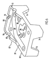
- Figure 6 shows an alternative embodiment of Figure 4 with an additional structure integrally molded with the support structure of the second shot injection molding process.
- In Figure 1, a
circuit pattern 30 is formed by a first shot injection molding process in afirst mold cavity 32. A preferred first electrically insulatingmaterial 34 selected for this circuit pattern is polyethersulfone with a catalyst. A suitable polyethersulfone is Victrex® 4100 G, one suitable filler catalyst is a palladium catalyst dispersed on a powdered aluminum silicate clay as is disclosed in US Patent 3 600 330 by Examples 6 and 9. The catalyst mixed into the first electrically insulatingmaterial 34 catalyzes the material for electroless metal deposition in subsequent steps in the process. The electrically insulatingmaterial 34 can be treated by a minimal series of steps to add metal for forming electricallyconductive paths 36 in a printed circuit board. Adhesion promotion of insulating materials containing the catalyst, herein also referred to as adhesion promotion catalyst activation process, activates the material for electroless metal deposition. Approximately 20% glass filler can be added to the electrically insulatingmaterial 34. However, the metal surfaces formed on the base material are smoother when using polyethersulfone without glass filler. - Other suitable electrically insulating materials for the
circuit pattern 30 are ceramics, thermoset polymers and high temperature thermoplastic materials selected from a group consisting of polysulfone, polyethermimide, polyethersulfone, polyphenylene sulfide and polyetheretherketone. - Referring to Figure 2, the
circuit pattern 30 has serveralfull surface sections 38 on a first orcomponent side 40. - Some of the
full surface sections 38 haveholes 42 which typically extend all the way through the thickness of thecircuit pattern 30. Theholes 42, formed by pins 43 (Fig. 1) haveinterior walls 44 for treatment to form electricallyconductive paths 36 through the thickness of thecircuit pattern 30. Thecircuit pattern 30 has aweb portion 46 for connecting thefull surface sections 38 to each other and for spacing thefull surface sections 38 relative to each other. Theweb portion 46 is recessed below thefull surface sections 38. - A second or
solder side 48 of thecircuit pattern 30 has several full surface sections 50 (only one shown). Theweb portion 46 connects thefull surface sections 50 to each other and spaces thefull surface sections 50 relative to each other. Thecircuit pattern 30 having thefull surface sections 38, thefull surface sections 50 and theweb portion 46 fabricated by the first shot injection molding process forms a one-piece integral unit. - A feature of this invention is that the
web portion 46 provides a rigid connecting structure between thefull surface sections 38 on thecomponent side 40 and thefull surface sections 50 on thesolder side 48 as well as between the severalfull surface sections - Another feature of this invention is that the
circuit pattern 30 with theweb portion 46 can be used as both the circuit pattern and an insulating substrate by selective treatment of thecircuit pattern 30 to form electricallyconductive paths 36. - In Figure 3, the
circuit pattern 30 has been removed from thefirst mold cavity 32 and inserted into asecond mold cavity 52. Asupport structure 54 is formed by a second shot injection molding Process in thesecond mold cavity 52 and onto themolded circuit pattern 30. A preferred second electrically insulatingmaterial 56 selected for thesupport structure 54 is polyethersulfone (Victrex® 200P without catalyst). The electrically insulatingmaterial 56 may be with glass, mineral or other fillers. It is believed that it is preferable to use reinforcing fillers in this material to provide rigidity to thesupport structure 54. Other suitable materials for the second insulating material include ceramics, thermoset resins, and high temperature thermoplastic materials including polyesters. - The electrically insulating
material 56 of thesupport structure 54 covers theweb portion 46 on thecomponent side 40 and on thesolder side 48 of thecircuit pattern 30 while leaving thefull surface sections - The electrically insulating
material 56 of thesupport structure 54 is prevented from entering theholes 42 of thecircuit pattern 30 by thesecond cavity mold 52. The electrically insulatingmaterial 56 also forms aborder 58 around the periphery of thecircuit pattern 30. Thesupport structure 54 with thecircuit pattern 30 is removed from thesecond cavity mold 52 and is ready for further processing (Figure 4). - Another feature of the invention is that the
support structure 54 is rigidly connected to thecircuit pattern 30 by covering theweb portion 46 on thecomponent side 40 and thesolder side 48 and by forming aborder 58 around the periphery of thecircuit pattern 30. - In Figure 4, an alternate method of the invention is forming the
support structure 54 by a first shot injection molding process in a first mold cavity and forming thecircuit pattern 30 by a second shot injection molding process in a second mold cavity while maintaining the rigid connection structure between thecircuit pattern 30 and thesupport structure 54. Preferably, the second shot would comprise more than one molded shape. - A layer of
metal 59, such as copper, is adhered to thecircuit pattern 30 as shown in Figure 5 to form electricallyconductive paths 36 by subsequent steps in the process. - Since the
first material 34 is capable of adherent metallization and thesecond material 56 is incapable of being adherently metallized, themetal 59 adheres only to thecircuit pattern 30 formed from thefirst material 34. - In Figure 6, another embodiment of the invention is a
support structure 60. Thesupport structure 54 of Figure 4 has a rigid flat structure which is typical for printed circuit boards. Thesupport structure 60 has three-dimensional additional integrally moldedstructure 62 for mounting non-electrical components such as shafts, brackets, and the like, or for use as spacers, stand-offs, and the like. Thestructure 62 is molded from the electrically insulatingplastic material 56. The moldedstructure 62 avoids costly secondary operations such as attaching independently made brackets, frames, and the like, to provide the same result. Thestructure 62 has a firstupstanding wall 64 with a circular recess 66 therein for supporting a non-electrical component such as a cylindrical shaft. A secondupstanding wall 68 has varyingsized notches 70 for supporting rectangularly shaped components. A thirdupstanding wall 72 is similar to the firstupstanding wall 64.Several legs 74 extend downward from thecircuit pattern 30. Thelegs 74 can be used as spacers for spacing thecircuit pattern 30 from other structures in any machine or apparatus. Theupstanding walls legs 74 are examples of varying structures which can be integrally molded with the second shot injection molding process to reduce or avoid the cost of secondary operations such as adding independently made support brackets, frames, and the like. - The
support structure 60 can be treated by the same process as thesupport structure 54 to form the electricallyconductive paths 36. - Even though the molding process described is injection molding, the
circuit pattern 30, thesupport structure 54, the first shape 82 and the second shape 104 can also be formed by compression, casting and other molding processes. - The selected first
plastic material 43 and the secondplastic material 56 are thermoplastics. Other materials could be used by this invention such as thermoset resins, ceramics, glass, and the like. - To add the
metal 59 to the circuit pattern 30 (Fig. 5) for forming electricallyconductive paths 36, a few process steps are taken, as described in the following examples. - The
circuit pattern 30 was molded with polyethersulfone resin (Victrex® P200) containing 15% of a palladium treated clay filler. The clay filler contains 0.1% palladium by weight. Thesupport structure 54 was molded with clear polyethersulfone resin without filler. - The molded article was stress relieved by placing it in an oven; raising the oven temperature to 205°C; holding the article at that temperature for four hours; and then cooling the article in the oven.
- After the article was stress relieved, it was adhesion promoted by the following procedure:
-
1. Immerse for 1 minute in a solution of 90% dimethylformamide and 10% water.
2. Immerse for 1 minute in an aqueous 0.4 g/l solution of Gafac® RE610 at 60°C.
3. Immerse for 1 minute in an aqueous solution of 48% sulfuric acid at 60°C.
4. Etch for 2 minutes at 60°C in an aqueous solution containingchromium trioxide 400 g/l sulfuric acid 450 g/l Perfluoroalkysulfonate 0.5 g/l
5. Rinse in a dragout rinse.
6. Neutralize the residual chromium by immersion for 5 minutes in a solution of 1.8% sulfuric acid and 1.4% hydrogen peroxide.
7. Repeat step 6 in another neutralizing solution of the same composition.
8. Rinse in water for 2 minutes. - The adhesion promotion process made the surface of the article microporous and hydrophilic, and exposed the catalyst on the
surface sections hole walls 44 of thecircuit pattern 30. All the surfaces of the article, which were smooth and shiny before adhesion promotion, assumed a matte appearance. Thesurfaces - The molded article was immersed in an electroless copper plating solution for 1 hour to deposit a layer of copper 3 »m thick on the
surface sections hole walls 44. The article was then rinsed; dried at 65°C for 30 minutes; immersed in dichloromethane vapors over boiling dichloromethane liquid; and dried again at 60°C for 30 minutes. In this process, the matte, hydrophilic surface ofsupport structure 54 is made smooth, hydrophobic and resistant to extraneous metal deposition. - The molded article was then cleaned in a hot alkaline soak cleaner, rinsed, deoxidized in dilute sulfuric acid and returned to the electroless copper plating solution to deposit 25 »m of
metal 59, such as copper, on thesurface sections hole walls 44 thus completing the adherent metallization step to form the electricallyconductive paths 36. - The procedures of Example 1 are repeated using electroless nickel plating instead of electroless copper plating.
- It can now be easily understood that the method for molding an article for adherent metallization formed from electrically insulating materials, such as a printed circuit board, has been significantly simplified by the present invention. Forming a
circuit pattern 30 by a first shot injection molding process and interconnecting asupport structure 54 or substrate to thecircuit pattern 30 by using a second shot injection molding process to electrically insulate thecircuit pattern 30, except for selectedsurface areas conductive paths 36. This simplified method is particularly advantageous when producing these articles in high quantities. - This simplified method is further advantageous by being capable of integrally molding additional structures with the second shot injection molding process for mounting or attaching to non-electrical components.
Claims (14)
- A process for producing a unitary non-conductive article comprising an electric circuit pattern, said process comprising the steps of molding a first insulating material into at least one first predetermined shape, said first material comprising a filler catalyst for adherent metallization and capable to be catalyst-activated by an adhesion promotion catalyst activation process; molding a second electrically insulating material into at least one second predetermined shape, said second material being non-catalytic for adherent metallization and incapable to be catalyst-activated by the said adhesion promotion catalyst activation process; interconnecting said first and second shape to produce the unitary, one-piece, non-conductive article wherein selected surface areas of said article defined by exposed portions of the said first material are suitable for adherent metallization; exposing the surface of said article to the adhesion promotion catalyst activation process; and forming an adherent metal deposit on said exposed portions of said first insulating material.
- A process for producing a unitary non-conductive article comprising an electric circuit pattern, said process comprising the steps of molding a first insulating material into at least one first predetermined shape, said first material being non-catalytic for adherent metallization and incapable to be catalyst-activated by an adhesion promotion catalyst activation process; molding a second electrically insulating material into at least one second predetermined shape, said second material comprising a filler catalyst for adherent metallization and capable to be catalyst-activated by the said adhesion promotion catalyst activation process; interconnecting said first and second shape to produce the unitary, one-piece, non-conductive article wherein selected surface areas of said article defined by exposed portions of the said second material are suitable for adherent metallization; exposing the surface of said article to the adhesion promotion catalyst activation process; and forming an adherent metal deposit on said exposed portions of said second material.
- The process of claim 1 or 2 wherein the molding process is injection molding.
- The process of claims 1 to 3 wherein said first and second materials are selected form the group consisting of thermoplastic polymers, thermoset plastics, and ceramic materials.
- The process of claim 4 wherein the thermoplastic polymers are selected from polyesters, polyetheretherketones, polyetherimides, polyethersulfones, polyphenylene sulfides and polysulfones.
- The process of claims 1 to 5 wherein said catalytic material comprises a palladium catalyst.
- The process of claim 6 wherein said palladium catalyst is dispersed in a filler consisting of powdered aluminum silicate clay.
- A molded unitary article comprising an electric circuit pattern, said article comprising at least a first predetermined shape comprised of a first electrically insulating material comprising a filler catalyst and capable to be catalyst activated by an adhesion promotion process causing catalyst activation; at least a second predetermined shape comprised of a second electrically insulating material, said material being free of a filler catalyst; said first and said second materials defining first and second patterns on a surface of the molded article, said first pattern being suitable for adherent metallization and said second pattern being resistant to adherent metallization; and a metal layer adhered to said first pattern with the second pattern completely free of metal deposit.
- The article of claim 8 wherein said filler catalyst comprises powdered aluminum silicate clay having dispersed in it a palladium catalyst.
- The article of claim 8 or 9 wherein said first and second material comprise high temperature thermoplastic polymers.
- The article of claim 10 wherein the high temperature thermoplastic polymers are selected from polyesters, polysulfones, polyetherimides, polyethersulfones, polyphenylene sulfides, and polyetheretherketones.
- The article of one or more of claims 8 to 11 wherein said second material has been molded onto said first material.
- The article of one or more of claims 8 to 11 wherein said first material has been molded onto said second material.
- The article of claim 8 wherein the second shape molded onto the first shape is defining on the surface of the molded article the preselected insulating pattern outlining the conductive circuit pattern of an electric conductor network.
Applications Claiming Priority (2)
| Application Number | Priority Date | Filing Date | Title |
|---|---|---|---|
| US70444085A | 1985-02-22 | 1985-02-22 | |
| US704440 | 1985-02-22 |
Publications (3)
| Publication Number | Publication Date |
|---|---|
| EP0192233A2 EP0192233A2 (en) | 1986-08-27 |
| EP0192233A3 EP0192233A3 (en) | 1988-11-02 |
| EP0192233B1 true EP0192233B1 (en) | 1995-04-19 |
Family
ID=24829491
Family Applications (1)
| Application Number | Title | Priority Date | Filing Date |
|---|---|---|---|
| EP86102055A Expired - Lifetime EP0192233B1 (en) | 1985-02-22 | 1986-02-18 | Molded metallized articles and processes for making the same |
Country Status (6)
| Country | Link |
|---|---|
| EP (1) | EP0192233B1 (en) |
| JP (1) | JP2668112B2 (en) |
| AT (1) | ATE121463T1 (en) |
| CA (1) | CA1255810A (en) |
| DE (1) | DE3605342A1 (en) |
| GB (1) | GB2171355B (en) |
Families Citing this family (31)
| Publication number | Priority date | Publication date | Assignee | Title |
|---|---|---|---|---|
| JPH0665756B2 (en) * | 1986-06-24 | 1994-08-24 | 三共化成株式会社 | Partial plastic molded article and its manufacturing method |
| IN167760B (en) * | 1986-08-15 | 1990-12-15 | Kollmorgen Tech Corp | |
| JPH0660416B2 (en) * | 1986-11-18 | 1994-08-10 | 三共化成株式会社 | Manufacturing method of plastic molded products |
| JPS63130778A (en) * | 1986-11-21 | 1988-06-02 | Sankyo Kasei Kk | Production of plastic molding |
| JP2603828B2 (en) * | 1986-12-27 | 1997-04-23 | 三共化成 株式会社 | Manufacturing method of molded products such as circuit boards |
| US4812353A (en) * | 1986-12-27 | 1989-03-14 | Sankyo Kasei Kabushiki Kaisha | Process for the production of circuit board and the like |
| US4906802A (en) * | 1988-02-18 | 1990-03-06 | Neal Castleman | Molded chip carrier |
| US4872844A (en) * | 1988-07-08 | 1989-10-10 | Amp Incorporated | Component-carrying adapter for chip carrier socket |
| US4871319A (en) * | 1988-12-21 | 1989-10-03 | Amp Incorporated | Molded circuit board for ribbon cable connector |
| JP2726884B2 (en) * | 1989-04-07 | 1998-03-11 | 矢崎総業株式会社 | Method for manufacturing high-density wiring board |
| JP2816445B2 (en) * | 1989-05-18 | 1998-10-27 | 株式会社村田製作所 | Pyroelectric infrared detector |
| US5002493A (en) * | 1989-09-19 | 1991-03-26 | Amp Incorporated | Panel mounted electronic assembly |
| US5105055A (en) * | 1990-10-17 | 1992-04-14 | Digital Equipment Corporation | Tunnelled multiconductor system and method |
| FR2669576B1 (en) * | 1990-11-27 | 1994-11-18 | Eumail Sa | MOLDED PART HAVING A PARTIALLY METALLIZED FREE SURFACE AND PROCESS FOR OBTAINING SAME. |
| JPH0773155B2 (en) * | 1992-04-20 | 1995-08-02 | 大宏電機株式会社 | Method of manufacturing circuit parts |
| US5543725A (en) * | 1993-08-25 | 1996-08-06 | Sunright Limited | Reusable carrier for burn-in/testing on non packaged die |
| DE4416986A1 (en) * | 1993-10-29 | 1995-05-04 | Albert Schmidbauer | Process for producing from thermoplastic material a component having at least one integrated, electrically conducting section, and a component produced by this process |
| DE19544733A1 (en) * | 1995-11-30 | 1997-06-05 | Thomson Brandt Gmbh | Pressure injection moulding of mechanically complex circuit modules |
| JPH1012994A (en) * | 1996-06-24 | 1998-01-16 | Yazaki Corp | Method for producing molded article having conductive circuit |
| DE19704921C2 (en) * | 1997-02-10 | 1999-06-02 | Inotech Kunststofftechnik Gmbh | Electronic component |
| DE19707177A1 (en) * | 1997-02-22 | 1998-09-03 | Inotech Kunststofftechnik Gmbh | Choke coil inductance for electric circuit |
| EP1020947A3 (en) | 1998-12-22 | 2000-10-04 | Nokia Mobile Phones Ltd. | Method for manufacturing an antenna body for a phone and phone or handset having an internal antenna |
| GB2345022B (en) * | 1998-12-23 | 2003-06-11 | Nokia Mobile Phones Ltd | Method for manufacturing an antenna body for a phone |
| GB2349598A (en) * | 1999-01-22 | 2000-11-08 | Finglas Technologies Ltd | Moulded electrical components |
| DE10005029A1 (en) * | 2000-02-04 | 2001-08-09 | Abb Patent Gmbh | throttle |
| DE10234125A1 (en) * | 2002-07-26 | 2004-02-12 | Siemens Ag | Illuminatable plastic injection molding, comprises a display function with a visible surface region, an electroluminescent film, and a second surface region |
| WO2005086548A1 (en) | 2004-03-04 | 2005-09-15 | Sankyo Kasei Co., Ltd. | Three-dimensional circuit board |
| EP2033756A1 (en) * | 2007-09-05 | 2009-03-11 | Nederlandse Organisatie voor toegepast- natuurwetenschappelijk onderzoek TNO | A process for preparing a moulded product |
| DE102009035843A1 (en) * | 2009-07-31 | 2011-02-03 | Behr Gmbh & Co. Kg | Kühlerzargensystem |
| CN105092662B (en) * | 2014-05-20 | 2019-01-22 | 光宏精密股份有限公司 | electrochemical sensing test piece and manufacturing method thereof |
| DE102017124732B4 (en) | 2017-10-23 | 2025-03-06 | Richard Fritz Holding Gmbh | Window unit with decorative part and method for its production |
Family Cites Families (15)
| Publication number | Priority date | Publication date | Assignee | Title |
|---|---|---|---|---|
| DD11731A (en) * | ||||
| GB1254308A (en) * | 1968-12-19 | 1971-11-17 | Bakelite Xylonite Ltd | Selective plating of plastics mouldings |
| US3640789A (en) * | 1969-04-01 | 1972-02-08 | Furniture City Mfg Corp | Method of making metal-plated plastic articles |
| DE2207511A1 (en) * | 1972-02-17 | 1973-09-06 | Plated Plastic Developments Lt | Metal plating of non-conductors - by depositing catalyst on certain parts, followed by non-electrolytic plating |
| US3865623A (en) * | 1973-02-02 | 1975-02-11 | Litton Systems Inc | Fully additive process for manufacturing printed circuit boards |
| DE2305883A1 (en) * | 1973-02-07 | 1974-08-15 | Finsterhoelzl Rafi Elekt | CIRCUIT BOARD |
| JPS5141226A (en) * | 1974-10-02 | 1976-04-07 | Nippon Kokan Kk | ASHIBAKASETSUTETSUKYOSOCHI |
| US3982045A (en) * | 1974-10-11 | 1976-09-21 | Macdermid Incorporated | Method of manufacture of additive printed circuitboards using permanent resist mask |
| JPS51145866A (en) * | 1975-06-11 | 1976-12-15 | Tokyo Shibaura Electric Co | Circuit substrate manufacturing method |
| GB1499381A (en) * | 1975-07-29 | 1978-02-01 | Plessey Co Ltd | Printed circuit board switches |
| JPS5479474A (en) * | 1977-12-07 | 1979-06-25 | Citizen Watch Co Ltd | Circuit base for electronic watch |
| JPS5685894A (en) * | 1979-12-17 | 1981-07-13 | Tokyo Shibaura Electric Co | Method of forming printed circuit |
| DE3014041C2 (en) * | 1980-04-11 | 1982-04-08 | Braun Ag, 6000 Frankfurt | Method for applying electrically conductive tracks to a carrier made of insulating material |
| JPS587897A (en) * | 1981-07-06 | 1983-01-17 | シャープ株式会社 | Method of producing circuit wiring board |
| EP0132485A1 (en) * | 1983-07-21 | 1985-02-13 | Celluloid I Gislaved Ab | A method of producing chromium-plated plastics materials or plastics details, and an apparatus for carrying the method into effect |
-
1986
- 1986-02-14 GB GB8603699A patent/GB2171355B/en not_active Expired
- 1986-02-17 JP JP61033677A patent/JP2668112B2/en not_active Expired - Lifetime
- 1986-02-17 DE DE19863605342 patent/DE3605342A1/en not_active Withdrawn
- 1986-02-18 AT AT86102055T patent/ATE121463T1/en not_active IP Right Cessation
- 1986-02-18 EP EP86102055A patent/EP0192233B1/en not_active Expired - Lifetime
- 1986-02-21 CA CA000502428A patent/CA1255810A/en not_active Expired
Also Published As
| Publication number | Publication date |
|---|---|
| ATE121463T1 (en) | 1995-05-15 |
| JP2668112B2 (en) | 1997-10-27 |
| EP0192233A3 (en) | 1988-11-02 |
| JPS61239694A (en) | 1986-10-24 |
| EP0192233A2 (en) | 1986-08-27 |
| GB2171355A (en) | 1986-08-28 |
| CA1255810A (en) | 1989-06-13 |
| GB2171355B (en) | 1989-11-22 |
| DE3605342A1 (en) | 1986-09-04 |
| GB8603699D0 (en) | 1986-03-19 |
Similar Documents
| Publication | Publication Date | Title |
|---|---|---|
| EP0192233A2 (en) | Molded metallized articles and processes for making the same | |
| US5407622A (en) | Process for making metallized plastic articles | |
| KR960008311B1 (en) | Manufacturing method of plastic molding | |
| US4339303A (en) | Radiation stress relieving of sulfone polymer articles | |
| US4424095A (en) | Radiation stress relieving of polymer articles | |
| US5015519A (en) | Molded article with partial metal plating and a process for producing such article | |
| US4830880A (en) | Formation of catalytic metal nuclei for electroless plating | |
| US5233753A (en) | Method of making injection-moulded printed circuit boards | |
| US3854973A (en) | Method of making additive printed circuit boards | |
| US4602318A (en) | Substrates to interconnect electronic components | |
| CA1157622A (en) | Polysulfone surfaced laminated blanks | |
| GB2037488A (en) | Thermoplastics printed circuit board material | |
| US3799816A (en) | Metallizing insulating bases | |
| US4541882A (en) | Process for the manufacture of substrates to interconnect electronic components and articles made by said process | |
| US4374868A (en) | Method for producing printed circuit boards with punched holes having metallized walls | |
| US5863405A (en) | Process for forming conductive circuit on the surface of molded article | |
| JPH03204992A (en) | Swelling agent for pretreatment of syntheticresin before electroless metal, manufacture of wholly metallized substrate, wholly metallized substrate, and manufacture of printed wiring board, chip supporter, hybrid circuit, multilyered laminate semi-finished product, and electromagnetic shield semi-finished product | |
| JPS61288489A (en) | Manufacturing method of molded circuit board | |
| US4908259A (en) | Molded article with partial metal plating and a process for producing such article | |
| EP0397412A2 (en) | Electroless plating process | |
| JPH0570961A (en) | Catalyst for electroless plating, production of the same and its utilization method | |
| US3451131A (en) | Method for making an encapsulated electrical circuit module assembly | |
| JPH0779191B2 (en) | Manufacturing method of three-dimensional wiring board | |
| EP0732040B1 (en) | Method of making a printed circuit board | |
| JPH01207989A (en) | Plastic molded item |
Legal Events
| Date | Code | Title | Description |
|---|---|---|---|
| PUAI | Public reference made under article 153(3) epc to a published international application that has entered the european phase |
Free format text: ORIGINAL CODE: 0009012 |
|
| AK | Designated contracting states |
Kind code of ref document: A2 Designated state(s): AT CH FR IT LI NL SE |
|
| 17P | Request for examination filed |
Effective date: 19870211 |
|
| PUAL | Search report despatched |
Free format text: ORIGINAL CODE: 0009013 |
|
| AK | Designated contracting states |
Kind code of ref document: A3 Designated state(s): AT CH FR IT LI NL SE |
|
| RAP1 | Party data changed (applicant data changed or rights of an application transferred) |
Owner name: KOLLMORGEN CORPORATION Owner name: SMITH CORONA CORPORATION |
|
| 17Q | First examination report despatched |
Effective date: 19911024 |
|
| RAP1 | Party data changed (applicant data changed or rights of an application transferred) |
Owner name: AMP-AKZO CORPORATION (A DELAWARE CORP.) Owner name: SMITH CORONA CORPORATION |
|
| RAP1 | Party data changed (applicant data changed or rights of an application transferred) |
Owner name: AMP-AKZO CORPORATION (A DELAWARE CORP.) Owner name: SMITH CORONA CORPORATION |
|
| GRAA | (expected) grant |
Free format text: ORIGINAL CODE: 0009210 |
|
| AK | Designated contracting states |
Kind code of ref document: B1 Designated state(s): AT CH FR IT LI NL SE |
|
| PG25 | Lapsed in a contracting state [announced via postgrant information from national office to epo] |
Ref country code: IT Free format text: LAPSE BECAUSE OF FAILURE TO SUBMIT A TRANSLATION OF THE DESCRIPTION OR TO PAY THE FEE WITHIN THE PRE;WARNING: LAPSES OF ITALIAN PATENTS WITH EFFECTIVE DATE BEFORE 2007 MAY HAVE OCCURRED AT ANY TIME BEFORE 2007. THE CORRECT EFFECTIVE DATE MAY BE DIFFERENT FROM THE ONE RECORDED.SCRIBED TIME-LIMIT Effective date: 19950419 |
|
| REF | Corresponds to: |
Ref document number: 121463 Country of ref document: AT Date of ref document: 19950515 Kind code of ref document: T |
|
| PG25 | Lapsed in a contracting state [announced via postgrant information from national office to epo] |
Ref country code: SE Effective date: 19950719 |
|
| ET | Fr: translation filed | ||
| PLBE | No opposition filed within time limit |
Free format text: ORIGINAL CODE: 0009261 |
|
| STAA | Information on the status of an ep patent application or granted ep patent |
Free format text: STATUS: NO OPPOSITION FILED WITHIN TIME LIMIT |
|
| 26N | No opposition filed | ||
| PGFP | Annual fee paid to national office [announced via postgrant information from national office to epo] |
Ref country code: CH Payment date: 19960506 Year of fee payment: 15 |
|
| PGFP | Annual fee paid to national office [announced via postgrant information from national office to epo] |
Ref country code: FR Payment date: 19970224 Year of fee payment: 12 |
|
| PGFP | Annual fee paid to national office [announced via postgrant information from national office to epo] |
Ref country code: NL Payment date: 19970227 Year of fee payment: 12 |
|
| PG25 | Lapsed in a contracting state [announced via postgrant information from national office to epo] |
Ref country code: FR Free format text: THE PATENT HAS BEEN ANNULLED BY A DECISION OF A NATIONAL AUTHORITY Effective date: 19980228 |
|
| PG25 | Lapsed in a contracting state [announced via postgrant information from national office to epo] |
Ref country code: NL Free format text: LAPSE BECAUSE OF NON-PAYMENT OF DUE FEES Effective date: 19980901 |
|
| NLV4 | Nl: lapsed or anulled due to non-payment of the annual fee |
Effective date: 19980901 |
|
| REG | Reference to a national code |
Ref country code: FR Ref legal event code: ST |
|
| PGFP | Annual fee paid to national office [announced via postgrant information from national office to epo] |
Ref country code: AT Payment date: 19990107 Year of fee payment: 14 |
|
| PG25 | Lapsed in a contracting state [announced via postgrant information from national office to epo] |
Ref country code: AT Free format text: LAPSE BECAUSE OF NON-PAYMENT OF DUE FEES Effective date: 20000218 |
|
| PG25 | Lapsed in a contracting state [announced via postgrant information from national office to epo] |
Ref country code: CH Free format text: LAPSE BECAUSE OF NON-PAYMENT OF DUE FEES Effective date: 20010228 Ref country code: LI Free format text: LAPSE BECAUSE OF NON-PAYMENT OF DUE FEES Effective date: 20010228 |
|
| REG | Reference to a national code |
Ref country code: CH Ref legal event code: PL |