EP0189340B1 - Kommutierungskreis mit einer schnellen Diode und Mitteln zur Dämpfung der Schwingungen beim Öffnen des Kreises - Google Patents
Kommutierungskreis mit einer schnellen Diode und Mitteln zur Dämpfung der Schwingungen beim Öffnen des Kreises Download PDFInfo
- Publication number
- EP0189340B1 EP0189340B1 EP86400054A EP86400054A EP0189340B1 EP 0189340 B1 EP0189340 B1 EP 0189340B1 EP 86400054 A EP86400054 A EP 86400054A EP 86400054 A EP86400054 A EP 86400054A EP 0189340 B1 EP0189340 B1 EP 0189340B1
- Authority
- EP
- European Patent Office
- Prior art keywords
- diode
- fast
- supplementary
- current
- oscillations
- Prior art date
- Legal status (The legal status is an assumption and is not a legal conclusion. Google has not performed a legal analysis and makes no representation as to the accuracy of the status listed.)
- Expired
Links
- 230000010355 oscillation Effects 0.000 title claims description 8
- 238000013016 damping Methods 0.000 title description 3
- BASFCYQUMIYNBI-UHFFFAOYSA-N platinum Chemical compound [Pt] BASFCYQUMIYNBI-UHFFFAOYSA-N 0.000 claims description 6
- 239000004065 semiconductor Substances 0.000 claims description 6
- PCHJSUWPFVWCPO-UHFFFAOYSA-N gold Chemical compound [Au] PCHJSUWPFVWCPO-UHFFFAOYSA-N 0.000 claims description 3
- 239000010931 gold Substances 0.000 claims description 3
- 229910052737 gold Inorganic materials 0.000 claims description 3
- 229910052697 platinum Inorganic materials 0.000 claims description 3
- 238000005215 recombination Methods 0.000 claims description 3
- 230000006798 recombination Effects 0.000 claims description 3
- 238000011084 recovery Methods 0.000 description 5
- 238000009792 diffusion process Methods 0.000 description 3
- 230000002093 peripheral effect Effects 0.000 description 3
- 230000007704 transition Effects 0.000 description 3
- 238000004804 winding Methods 0.000 description 3
- 230000000903 blocking effect Effects 0.000 description 2
- 239000003990 capacitor Substances 0.000 description 2
- 239000000969 carrier Substances 0.000 description 2
- 239000012535 impurity Substances 0.000 description 2
- 230000001939 inductive effect Effects 0.000 description 2
- 230000002159 abnormal effect Effects 0.000 description 1
- 230000003416 augmentation Effects 0.000 description 1
- 239000004020 conductor Substances 0.000 description 1
- 230000007423 decrease Effects 0.000 description 1
- 238000010586 diagram Methods 0.000 description 1
- 230000000694 effects Effects 0.000 description 1
- 238000001465 metallisation Methods 0.000 description 1
- 238000000034 method Methods 0.000 description 1
- 230000003071 parasitic effect Effects 0.000 description 1
- 230000001681 protective effect Effects 0.000 description 1
- 239000000758 substrate Substances 0.000 description 1
- DPJRMOMPQZCRJU-UHFFFAOYSA-M thiamine hydrochloride Chemical compound Cl.[Cl-].CC1=C(CCO)SC=[N+]1CC1=CN=C(C)N=C1N DPJRMOMPQZCRJU-UHFFFAOYSA-M 0.000 description 1
Images
Classifications
-
- H—ELECTRICITY
- H02—GENERATION; CONVERSION OR DISTRIBUTION OF ELECTRIC POWER
- H02H—EMERGENCY PROTECTIVE CIRCUIT ARRANGEMENTS
- H02H9/00—Emergency protective circuit arrangements for limiting excess current or voltage without disconnection
- H02H9/005—Emergency protective circuit arrangements for limiting excess current or voltage without disconnection avoiding undesired transient conditions
-
- H—ELECTRICITY
- H02—GENERATION; CONVERSION OR DISTRIBUTION OF ELECTRIC POWER
- H02M—APPARATUS FOR CONVERSION BETWEEN AC AND AC, BETWEEN AC AND DC, OR BETWEEN DC AND DC, AND FOR USE WITH MAINS OR SIMILAR POWER SUPPLY SYSTEMS; CONVERSION OF DC OR AC INPUT POWER INTO SURGE OUTPUT POWER; CONTROL OR REGULATION THEREOF
- H02M3/00—Conversion of DC power input into DC power output
- H02M3/22—Conversion of DC power input into DC power output with intermediate conversion into AC
- H02M3/24—Conversion of DC power input into DC power output with intermediate conversion into AC by static converters
- H02M3/28—Conversion of DC power input into DC power output with intermediate conversion into AC by static converters using discharge tubes with control electrode or semiconductor devices with control electrode to produce the intermediate AC
- H02M3/325—Conversion of DC power input into DC power output with intermediate conversion into AC by static converters using discharge tubes with control electrode or semiconductor devices with control electrode to produce the intermediate AC using devices of a triode or a transistor type requiring continuous application of a control signal
- H02M3/335—Conversion of DC power input into DC power output with intermediate conversion into AC by static converters using discharge tubes with control electrode or semiconductor devices with control electrode to produce the intermediate AC using devices of a triode or a transistor type requiring continuous application of a control signal using semiconductor devices only
- H02M3/33538—Conversion of DC power input into DC power output with intermediate conversion into AC by static converters using discharge tubes with control electrode or semiconductor devices with control electrode to produce the intermediate AC using devices of a triode or a transistor type requiring continuous application of a control signal using semiconductor devices only of the forward type
-
- H—ELECTRICITY
- H02—GENERATION; CONVERSION OR DISTRIBUTION OF ELECTRIC POWER
- H02M—APPARATUS FOR CONVERSION BETWEEN AC AND AC, BETWEEN AC AND DC, OR BETWEEN DC AND DC, AND FOR USE WITH MAINS OR SIMILAR POWER SUPPLY SYSTEMS; CONVERSION OF DC OR AC INPUT POWER INTO SURGE OUTPUT POWER; CONTROL OR REGULATION THEREOF
- H02M7/00—Conversion of AC power input into DC power output; Conversion of DC power input into AC power output
- H02M7/02—Conversion of AC power input into DC power output without possibility of reversal
- H02M7/04—Conversion of AC power input into DC power output without possibility of reversal by static converters
- H02M7/06—Conversion of AC power input into DC power output without possibility of reversal by static converters using discharge tubes without control electrode or semiconductor devices without control electrode
- H02M7/062—Avoiding or suppressing excessive transient voltages or currents
-
- H—ELECTRICITY
- H03—ELECTRONIC CIRCUITRY
- H03K—PULSE TECHNIQUE
- H03K17/00—Electronic switching or gating, i.e. not by contact-making and –breaking
- H03K17/16—Modifications for eliminating interference voltages or currents
-
- H—ELECTRICITY
- H10—SEMICONDUCTOR DEVICES; ELECTRIC SOLID-STATE DEVICES NOT OTHERWISE PROVIDED FOR
- H10D—INORGANIC ELECTRIC SEMICONDUCTOR DEVICES
- H10D84/00—Integrated devices formed in or on semiconductor substrates that comprise only semiconducting layers, e.g. on Si wafers or on GaAs-on-Si wafers
- H10D84/201—Integrated devices formed in or on semiconductor substrates that comprise only semiconducting layers, e.g. on Si wafers or on GaAs-on-Si wafers characterised by the integration of only components covered by H10D1/00 or H10D8/00, e.g. RLC circuits
- H10D84/204—Integrated devices formed in or on semiconductor substrates that comprise only semiconducting layers, e.g. on Si wafers or on GaAs-on-Si wafers characterised by the integration of only components covered by H10D1/00 or H10D8/00, e.g. RLC circuits of combinations of diodes or capacitors or resistors
- H10D84/221—Integrated devices formed in or on semiconductor substrates that comprise only semiconducting layers, e.g. on Si wafers or on GaAs-on-Si wafers characterised by the integration of only components covered by H10D1/00 or H10D8/00, e.g. RLC circuits of combinations of diodes or capacitors or resistors of only diodes
Definitions
- the present invention relates to switching circuits such as converters, switching power supplies, choppers, inverters, etc.
- circuits often include rectifier diodes in series with inductive loads and it is necessary to use so-called fast diodes, that is to say diodes which quickly block when the voltage is reversed at their terminals.
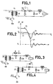
- FIG. 1 shows by way of example a rectification circuit placed at the terminals of the secondary winding ES of the output transformer TS of a switching power supply (the primary winding EP being in series with a switch Tp actuated at the frequency cutting).
- This circuit includes for example a fast rectifying diode D1 in series between the secondary winding ES and the inductive load L, R and another diode D2 in parallel with the load only.
- a stray inductance (wiring inductance) and a stray capacitance (of the diode D1) have been shown in dotted lines in FIG. 1.
- FIG. 2 shows the waveforms of the current 11 in the rectifying diode D1 and the voltage V1 at its terminals at the time of switching, that is to say at the time of the transition transition from one.
- direct current Id. important at zero current and low direct voltage Vd at high negative reverse voltage Vi.
- This transition presents significant oscillations which would have to be damped strongly without however creating excessively large losses and without using a large number of components.
- the present invention proposes to put in parallel on the fast rectifying diode D1 a "slow" diode D3.
- This diode D3 has a much smaller junction surface than that of the fast diode D1 and a switching speed towards the blocked state is also significantly lower than that of the diode D1.
- patent FR 2 405 576 which shows a protective diode in parallel with another. But it is surge protection and the protection diode is a fast diode.
- FIG. 4 is identical to FIG. 3 except that all of the resistor R and of the capacitor C is replaced by a diode D3, slower and with a smaller junction surface than the diode D1, in parallel on diode D1.
- the recovery time of the slow diode being typically a few microseconds while that of the fast diode is a few tens of nanosecond (time between the first negative current peak and the first zero crossing following this peak).
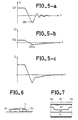
- FIG. 6 represents a simple embodiment: the diodes are constituted by separate semiconductor pads soldered on the same support so that they can be mounted in a single housing (thus allowing a limitation of the wiring inductances).
- Diode D1 is doped with gold or platinum to accelerate the recombination of carriers present in the semiconductor regions just before blocking.
- diode D3 is not doped with gold or platinum, or it is only weakly doped.
- FIG. 7 proposes another embodiment: the two diodes are produced on the same semiconductor substrate.
- the central zone constitutes the fast diode D1
- the peripheral zone constitutes the slower diode D3.
- the area of the central zone is greater than that of the peripheral zone so that the main current flows through the diode D1.
- the thickness of the least doped area N is greater at the periphery than, in the central area, so that the lifetime of the carriers is longer in the area corresponding to the diode D3.
- diode D3 in integrated form or not, including an embodiment in which the diode D3 is constituted by the base collector junction of a transistor whose emitter is directly connected to a anode metallization of the diode: the overlap in this diode-mounted transistor is slower than in the main diode.
Landscapes
- Engineering & Computer Science (AREA)
- Power Engineering (AREA)
- Bipolar Integrated Circuits (AREA)
- Electronic Switches (AREA)
- Dc-Dc Converters (AREA)
- Semiconductor Integrated Circuits (AREA)
Claims (3)
Applications Claiming Priority (2)
| Application Number | Priority Date | Filing Date | Title |
|---|---|---|---|
| FR8500522A FR2576164B1 (fr) | 1985-01-15 | 1985-01-15 | Circuit de commutation utilisant une diode rapide et pourvu de moyens d'amortissement des oscillations a l'ouverture |
| FR8500522 | 1985-01-15 |
Publications (2)
| Publication Number | Publication Date |
|---|---|
| EP0189340A1 EP0189340A1 (de) | 1986-07-30 |
| EP0189340B1 true EP0189340B1 (de) | 1989-05-17 |
Family
ID=9315293
Family Applications (1)
| Application Number | Title | Priority Date | Filing Date |
|---|---|---|---|
| EP86400054A Expired EP0189340B1 (de) | 1985-01-15 | 1986-01-10 | Kommutierungskreis mit einer schnellen Diode und Mitteln zur Dämpfung der Schwingungen beim Öffnen des Kreises |
Country Status (5)
| Country | Link |
|---|---|
| US (1) | US4688157A (de) |
| EP (1) | EP0189340B1 (de) |
| JP (1) | JPH0622321B2 (de) |
| DE (1) | DE3663432D1 (de) |
| FR (1) | FR2576164B1 (de) |
Families Citing this family (15)
| Publication number | Priority date | Publication date | Assignee | Title |
|---|---|---|---|---|
| JPH01113587U (de) * | 1988-01-25 | 1989-07-31 | ||
| DE4135259C1 (de) * | 1991-10-25 | 1993-01-07 | Semikron Elektronik Gmbh, 8500 Nuernberg, De | |
| DE4209214C2 (de) * | 1992-03-21 | 1995-12-14 | Ant Nachrichtentech | Anordnung zur Begrenzung von Überspannungen |
| US5313381A (en) * | 1992-09-01 | 1994-05-17 | Power Integrations, Inc. | Three-terminal switched mode power supply integrated circuit |
| US5483411A (en) * | 1993-04-22 | 1996-01-09 | Sturman; Oded E. | Chatterless low power AC solenoid without pole shading |
| US5672988A (en) * | 1994-04-15 | 1997-09-30 | Linear Technology Corporation | High-speed switching regulator drive circuit |
| US5689409A (en) * | 1994-07-27 | 1997-11-18 | Deutsche Thomson-Brandt Gmbh | Switched-mode power supply |
| GB2318927B (en) * | 1996-10-30 | 2000-09-27 | Pi Electronics | Voltage clamp |
| DE19732766C2 (de) | 1997-07-30 | 2000-11-30 | Mirow Georg Dieter | Spannungsversorgung für einen Sensor |
| US6088247A (en) * | 1997-10-29 | 2000-07-11 | Pi Electronics (H. K.) Limited | Voltage clamp |
| CA2377503A1 (en) | 1999-06-30 | 2001-01-11 | Peco Ii, Inc. | Diode recovery current suppression circuits |
| JP3981886B2 (ja) * | 2003-03-11 | 2007-09-26 | 株式会社デンソー | 整流回路 |
| US20050248963A1 (en) * | 2004-05-07 | 2005-11-10 | Cheng Chung Y | Circuit for controlling the reverse recovery current in a blocking diode |
| US7375984B2 (en) | 2006-06-16 | 2008-05-20 | Astec Custom Power (Hk) Ltd. | Zero voltage zero current switching converter |
| US20080071887A1 (en) * | 2006-09-19 | 2008-03-20 | Microsoft Corporation | Intelligent translation of electronic data interchange documents to extensible markup language representations |
Family Cites Families (6)
| Publication number | Priority date | Publication date | Assignee | Title |
|---|---|---|---|---|
| CA734084A (en) * | 1966-05-10 | N.V. Philips Gloeilampenfabrieken | Rectifying device | |
| US2895100A (en) * | 1955-12-17 | 1959-07-14 | Siemens Ag | Semiconductor junction-type rectifier systems |
| US3418587A (en) * | 1965-06-04 | 1968-12-24 | American Electronic Lab | High sensitivity and power signal detecting device |
| FR2405576A1 (fr) * | 1977-10-07 | 1979-05-04 | Lignes Telegraph Telephon | Circuit de protection d'une diode schottky de puissance contre les surtensions inverses transitoires |
| DE2915837A1 (de) * | 1979-04-17 | 1980-10-30 | Karl Dipl Ing Dillnberger | Energiesparende netzgleichrichteranordnung |
| JPS5688675A (en) * | 1979-12-19 | 1981-07-18 | Tsuneo Ikegami | Rectifier |
-
1985
- 1985-01-15 FR FR8500522A patent/FR2576164B1/fr not_active Expired
-
1986
- 1986-01-07 US US06/816,716 patent/US4688157A/en not_active Expired - Lifetime
- 1986-01-10 EP EP86400054A patent/EP0189340B1/de not_active Expired
- 1986-01-10 DE DE8686400054T patent/DE3663432D1/de not_active Expired
- 1986-01-13 JP JP61004882A patent/JPH0622321B2/ja not_active Expired - Lifetime
Also Published As
| Publication number | Publication date |
|---|---|
| JPH0622321B2 (ja) | 1994-03-23 |
| US4688157A (en) | 1987-08-18 |
| DE3663432D1 (en) | 1989-06-22 |
| EP0189340A1 (de) | 1986-07-30 |
| FR2576164A1 (fr) | 1986-07-18 |
| FR2576164B1 (fr) | 1987-02-20 |
| JPS61169018A (ja) | 1986-07-30 |
Similar Documents
| Publication | Publication Date | Title |
|---|---|---|
| EP0189340B1 (de) | Kommutierungskreis mit einer schnellen Diode und Mitteln zur Dämpfung der Schwingungen beim Öffnen des Kreises | |
| EP0579561B1 (de) | Schutzschaltung gegen Überspannungen für Leistungsbauteil | |
| CA2319267A1 (fr) | Procede de symetrisation de defauts asymetriques | |
| EP2092643B1 (de) | Glied für eine synchron-gleichrichterbrücke, diesbezügliche synchron-gleichrichterbrücke und verwendung dafür | |
| EP0359680B1 (de) | Integrierbare, aktive Diode | |
| FR2572600A1 (fr) | Stabilisateur electronique de tension, utilisable en particulier dans l'automobile, avec protection contre les surtensions transitoires de polarite opposee a celle du generateur | |
| FR2475825A1 (fr) | Dispositif electronique de commutation a effet de proximite, protege contee les impulsions parasites | |
| FR2520950A1 (fr) | Circuit redresseur en pont de transistors, avec protection contre les surintensites, a usage telephonique | |
| EP0146183B1 (de) | Schnittstellenanordnung für eine Teilnehmersprechstelle | |
| FR3147450A1 (fr) | Circuit de protection contre les surtensions | |
| EP0881682B1 (de) | Hochspannungsschutzanordnung für einen integrierten MOS-Leistungstransistor | |
| EP0619637B1 (de) | Schutz eines Kraftfahrzeugdrehstromgenerators | |
| EP0370896B1 (de) | Leistungs-Schalteinrichtung, insbesondere für Umrichter | |
| FR2535551A1 (fr) | Dispositif de commutation electronique a faible dissipation de puissance | |
| EP4199345A1 (de) | Vorrichtung und verfahren zur überwachung eines elektrischen energiewandlers, zugehöriges elektrisches energieumwandlungssystem | |
| FR2574232A1 (fr) | Circuit integre monolithique, protege a l'egard d'une inversion de polarite | |
| EP3972111A1 (de) | Steuerung von zwei in reihe geschalteten schaltern | |
| EP2751917B1 (de) | Leistungsstarker wandler mit niedrigenergieschalter und schaltsteuerungsvorrichtung zur erzeugung eines pulses mit einem referenzwert und mindestens zwei steuerwerten | |
| CA2729177C (fr) | Circuit d'amortissement actif pour un circuit electrique de decoupage | |
| EP1710913B1 (de) | Getakte Stromversorgung | |
| FR3112436A1 (fr) | Dispositif de protection d’un circuit de distribution d’une énergie électrique | |
| FR2608320A1 (fr) | Dispositif de protection contre les surtensions a faible capacite | |
| FR2790341A1 (fr) | Alternateur equipe de moyens perfectionnes de protection contre le delestage de charges, et dispositif regulateur associe | |
| JPH0513681A (ja) | 過電流保護回路と半導体装置 | |
| FR2535900A1 (fr) | Appareil bipolaire a semi-conducteurs |
Legal Events
| Date | Code | Title | Description |
|---|---|---|---|
| PUAI | Public reference made under article 153(3) epc to a published international application that has entered the european phase |
Free format text: ORIGINAL CODE: 0009012 |
|
| AK | Designated contracting states |
Kind code of ref document: A1 Designated state(s): CH DE FR GB IT LI NL |
|
| 17P | Request for examination filed |
Effective date: 19860808 |
|
| 17Q | First examination report despatched |
Effective date: 19880225 |
|
| GRAA | (expected) grant |
Free format text: ORIGINAL CODE: 0009210 |
|
| ITF | It: translation for a ep patent filed | ||
| AK | Designated contracting states |
Kind code of ref document: B1 Designated state(s): CH DE FR GB IT LI NL |
|
| PG25 | Lapsed in a contracting state [announced via postgrant information from national office to epo] |
Ref country code: NL Effective date: 19890517 |
|
| RAP4 | Party data changed (patent owner data changed or rights of a patent transferred) |
Owner name: THOMSON-CSF |
|
| GBT | Gb: translation of ep patent filed (gb section 77(6)(a)/1977) | ||
| REF | Corresponds to: |
Ref document number: 3663432 Country of ref document: DE Date of ref document: 19890622 |
|
| NLV1 | Nl: lapsed or annulled due to failure to fulfill the requirements of art. 29p and 29m of the patents act | ||
| PLBE | No opposition filed within time limit |
Free format text: ORIGINAL CODE: 0009261 |
|
| STAA | Information on the status of an ep patent application or granted ep patent |
Free format text: STATUS: NO OPPOSITION FILED WITHIN TIME LIMIT |
|
| 26N | No opposition filed | ||
| ITTA | It: last paid annual fee | ||
| PGFP | Annual fee paid to national office [announced via postgrant information from national office to epo] |
Ref country code: CH Payment date: 19920120 Year of fee payment: 7 |
|
| PG25 | Lapsed in a contracting state [announced via postgrant information from national office to epo] |
Ref country code: LI Effective date: 19930131 Ref country code: CH Effective date: 19930131 |
|
| REG | Reference to a national code |
Ref country code: CH Ref legal event code: PL |
|
| REG | Reference to a national code |
Ref country code: FR Ref legal event code: D6 |
|
| PGFP | Annual fee paid to national office [announced via postgrant information from national office to epo] |
Ref country code: DE Payment date: 20010102 Year of fee payment: 16 |
|
| REG | Reference to a national code |
Ref country code: GB Ref legal event code: IF02 |
|
| PG25 | Lapsed in a contracting state [announced via postgrant information from national office to epo] |
Ref country code: DE Free format text: LAPSE BECAUSE OF NON-PAYMENT OF DUE FEES Effective date: 20020801 |
|
| PGFP | Annual fee paid to national office [announced via postgrant information from national office to epo] |
Ref country code: GB Payment date: 20030122 Year of fee payment: 18 |
|
| PGFP | Annual fee paid to national office [announced via postgrant information from national office to epo] |
Ref country code: FR Payment date: 20030128 Year of fee payment: 18 |
|
| PG25 | Lapsed in a contracting state [announced via postgrant information from national office to epo] |
Ref country code: GB Free format text: LAPSE BECAUSE OF NON-PAYMENT OF DUE FEES Effective date: 20040110 |
|
| GBPC | Gb: european patent ceased through non-payment of renewal fee |
Effective date: 20040110 |
|
| PG25 | Lapsed in a contracting state [announced via postgrant information from national office to epo] |
Ref country code: FR Free format text: LAPSE BECAUSE OF NON-PAYMENT OF DUE FEES Effective date: 20040930 |
|
| REG | Reference to a national code |
Ref country code: FR Ref legal event code: ST |
|
| PG25 | Lapsed in a contracting state [announced via postgrant information from national office to epo] |
Ref country code: IT Free format text: LAPSE BECAUSE OF NON-PAYMENT OF DUE FEES;WARNING: LAPSES OF ITALIAN PATENTS WITH EFFECTIVE DATE BEFORE 2007 MAY HAVE OCCURRED AT ANY TIME BEFORE 2007. THE CORRECT EFFECTIVE DATE MAY BE DIFFERENT FROM THE ONE RECORDED. Effective date: 20050110 |