EP4199345A1 - Vorrichtung und verfahren zur überwachung eines elektrischen energiewandlers, zugehöriges elektrisches energieumwandlungssystem - Google Patents
Vorrichtung und verfahren zur überwachung eines elektrischen energiewandlers, zugehöriges elektrisches energieumwandlungssystem Download PDFInfo
- Publication number
- EP4199345A1 EP4199345A1 EP22213560.0A EP22213560A EP4199345A1 EP 4199345 A1 EP4199345 A1 EP 4199345A1 EP 22213560 A EP22213560 A EP 22213560A EP 4199345 A1 EP4199345 A1 EP 4199345A1
- Authority
- EP
- European Patent Office
- Prior art keywords
- branch
- voltage
- detection
- switching
- impedance
- Prior art date
- Legal status (The legal status is an assumption and is not a legal conclusion. Google has not performed a legal analysis and makes no representation as to the accuracy of the status listed.)
- Pending
Links
- 238000006243 chemical reaction Methods 0.000 title claims description 31
- 238000012544 monitoring process Methods 0.000 title claims description 26
- 238000000034 method Methods 0.000 title claims description 14
- 238000001514 detection method Methods 0.000 claims abstract description 152
- 238000001914 filtration Methods 0.000 claims abstract description 43
- 238000012806 monitoring device Methods 0.000 claims abstract description 29
- 239000004065 semiconductor Substances 0.000 claims description 31
- 239000000463 material Substances 0.000 claims description 20
- JMASRVWKEDWRBT-UHFFFAOYSA-N Gallium nitride Chemical compound [Ga]#N JMASRVWKEDWRBT-UHFFFAOYSA-N 0.000 claims description 17
- 239000003990 capacitor Substances 0.000 claims description 16
- 230000003071 parasitic effect Effects 0.000 claims description 15
- HBMJWWWQQXIZIP-UHFFFAOYSA-N silicon carbide Chemical compound [Si+]#[C-] HBMJWWWQQXIZIP-UHFFFAOYSA-N 0.000 claims description 14
- XUIMIQQOPSSXEZ-UHFFFAOYSA-N Silicon Chemical compound [Si] XUIMIQQOPSSXEZ-UHFFFAOYSA-N 0.000 claims description 11
- 239000010703 silicon Substances 0.000 claims description 8
- 229910052710 silicon Inorganic materials 0.000 claims description 8
- 229910002601 GaN Inorganic materials 0.000 description 14
- 229910010271 silicon carbide Inorganic materials 0.000 description 10
- 230000002457 bidirectional effect Effects 0.000 description 6
- 235000021183 entrée Nutrition 0.000 description 5
- 238000005259 measurement Methods 0.000 description 4
- 230000003287 optical effect Effects 0.000 description 3
- 230000002441 reversible effect Effects 0.000 description 3
- GYHNNYVSQQEPJS-UHFFFAOYSA-N Gallium Chemical compound [Ga] GYHNNYVSQQEPJS-UHFFFAOYSA-N 0.000 description 2
- 239000004020 conductor Substances 0.000 description 2
- 230000005669 field effect Effects 0.000 description 2
- 229910052733 gallium Inorganic materials 0.000 description 2
- 230000007274 generation of a signal involved in cell-cell signaling Effects 0.000 description 2
- 238000002955 isolation Methods 0.000 description 2
- 244000045947 parasite Species 0.000 description 2
- 241001101998 Galium Species 0.000 description 1
- 230000000903 blocking effect Effects 0.000 description 1
- 230000006378 damage Effects 0.000 description 1
- 230000010365 information processing Effects 0.000 description 1
- 230000010354 integration Effects 0.000 description 1
- 229910044991 metal oxide Inorganic materials 0.000 description 1
- 150000004706 metal oxides Chemical class 0.000 description 1
- 150000004767 nitrides Chemical class 0.000 description 1
- 230000036632 reaction speed Effects 0.000 description 1
- 230000002123 temporal effect Effects 0.000 description 1
- 230000001052 transient effect Effects 0.000 description 1
Images


Classifications
-
- H—ELECTRICITY
- H02—GENERATION; CONVERSION OR DISTRIBUTION OF ELECTRIC POWER
- H02M—APPARATUS FOR CONVERSION BETWEEN AC AND AC, BETWEEN AC AND DC, OR BETWEEN DC AND DC, AND FOR USE WITH MAINS OR SIMILAR POWER SUPPLY SYSTEMS; CONVERSION OF DC OR AC INPUT POWER INTO SURGE OUTPUT POWER; CONTROL OR REGULATION THEREOF
- H02M3/00—Conversion of dc power input into dc power output
- H02M3/02—Conversion of dc power input into dc power output without intermediate conversion into ac
- H02M3/04—Conversion of dc power input into dc power output without intermediate conversion into ac by static converters
- H02M3/10—Conversion of dc power input into dc power output without intermediate conversion into ac by static converters using discharge tubes with control electrode or semiconductor devices with control electrode
- H02M3/145—Conversion of dc power input into dc power output without intermediate conversion into ac by static converters using discharge tubes with control electrode or semiconductor devices with control electrode using devices of a triode or transistor type requiring continuous application of a control signal
- H02M3/155—Conversion of dc power input into dc power output without intermediate conversion into ac by static converters using discharge tubes with control electrode or semiconductor devices with control electrode using devices of a triode or transistor type requiring continuous application of a control signal using semiconductor devices only
- H02M3/156—Conversion of dc power input into dc power output without intermediate conversion into ac by static converters using discharge tubes with control electrode or semiconductor devices with control electrode using devices of a triode or transistor type requiring continuous application of a control signal using semiconductor devices only with automatic control of output voltage or current, e.g. switching regulators
- H02M3/158—Conversion of dc power input into dc power output without intermediate conversion into ac by static converters using discharge tubes with control electrode or semiconductor devices with control electrode using devices of a triode or transistor type requiring continuous application of a control signal using semiconductor devices only with automatic control of output voltage or current, e.g. switching regulators including plural semiconductor devices as final control devices for a single load
- H02M3/1584—Conversion of dc power input into dc power output without intermediate conversion into ac by static converters using discharge tubes with control electrode or semiconductor devices with control electrode using devices of a triode or transistor type requiring continuous application of a control signal using semiconductor devices only with automatic control of output voltage or current, e.g. switching regulators including plural semiconductor devices as final control devices for a single load with a plurality of power processing stages connected in parallel
-
- G—PHYSICS
- G01—MEASURING; TESTING
- G01R—MEASURING ELECTRIC VARIABLES; MEASURING MAGNETIC VARIABLES
- G01R31/00—Arrangements for testing electric properties; Arrangements for locating electric faults; Arrangements for electrical testing characterised by what is being tested not provided for elsewhere
- G01R31/40—Testing power supplies
- G01R31/42—AC power supplies
-
- G—PHYSICS
- G01—MEASURING; TESTING
- G01R—MEASURING ELECTRIC VARIABLES; MEASURING MAGNETIC VARIABLES
- G01R19/00—Arrangements for measuring currents or voltages or for indicating presence or sign thereof
- G01R19/0092—Arrangements for measuring currents or voltages or for indicating presence or sign thereof measuring current only
-
- G—PHYSICS
- G01—MEASURING; TESTING
- G01R—MEASURING ELECTRIC VARIABLES; MEASURING MAGNETIC VARIABLES
- G01R19/00—Arrangements for measuring currents or voltages or for indicating presence or sign thereof
- G01R19/12—Measuring rate of change
-
- G—PHYSICS
- G01—MEASURING; TESTING
- G01R—MEASURING ELECTRIC VARIABLES; MEASURING MAGNETIC VARIABLES
- G01R19/00—Arrangements for measuring currents or voltages or for indicating presence or sign thereof
- G01R19/165—Indicating that current or voltage is either above or below a predetermined value or within or outside a predetermined range of values
- G01R19/16566—Circuits and arrangements for comparing voltage or current with one or several thresholds and for indicating the result not covered by subgroups G01R19/16504, G01R19/16528, G01R19/16533
- G01R19/16571—Circuits and arrangements for comparing voltage or current with one or several thresholds and for indicating the result not covered by subgroups G01R19/16504, G01R19/16528, G01R19/16533 comparing AC or DC current with one threshold, e.g. load current, over-current, surge current or fault current
-
- H—ELECTRICITY
- H01—ELECTRIC ELEMENTS
- H01L—SEMICONDUCTOR DEVICES NOT COVERED BY CLASS H10
- H01L29/00—Semiconductor devices specially adapted for rectifying, amplifying, oscillating or switching and having potential barriers; Capacitors or resistors having potential barriers, e.g. a PN-junction depletion layer or carrier concentration layer; Details of semiconductor bodies or of electrodes thereof ; Multistep manufacturing processes therefor
- H01L29/66—Types of semiconductor device ; Multistep manufacturing processes therefor
- H01L29/66007—Multistep manufacturing processes
- H01L29/66075—Multistep manufacturing processes of devices having semiconductor bodies comprising group 14 or group 13/15 materials
- H01L29/66083—Multistep manufacturing processes of devices having semiconductor bodies comprising group 14 or group 13/15 materials the devices being controllable only by variation of the electric current supplied or the electric potential applied, to one or more of the electrodes carrying the current to be rectified, amplified, oscillated or switched, e.g. two-terminal devices
- H01L29/6609—Diodes
- H01L29/66098—Breakdown diodes
- H01L29/66106—Zener diodes
-
- H—ELECTRICITY
- H01—ELECTRIC ELEMENTS
- H01L—SEMICONDUCTOR DEVICES NOT COVERED BY CLASS H10
- H01L29/00—Semiconductor devices specially adapted for rectifying, amplifying, oscillating or switching and having potential barriers; Capacitors or resistors having potential barriers, e.g. a PN-junction depletion layer or carrier concentration layer; Details of semiconductor bodies or of electrodes thereof ; Multistep manufacturing processes therefor
- H01L29/66—Types of semiconductor device ; Multistep manufacturing processes therefor
- H01L29/86—Types of semiconductor device ; Multistep manufacturing processes therefor controllable only by variation of the electric current supplied, or only the electric potential applied, to one or more of the electrodes carrying the current to be rectified, amplified, oscillated or switched
- H01L29/861—Diodes
- H01L29/866—Zener diodes
-
- H—ELECTRICITY
- H02—GENERATION; CONVERSION OR DISTRIBUTION OF ELECTRIC POWER
- H02M—APPARATUS FOR CONVERSION BETWEEN AC AND AC, BETWEEN AC AND DC, OR BETWEEN DC AND DC, AND FOR USE WITH MAINS OR SIMILAR POWER SUPPLY SYSTEMS; CONVERSION OF DC OR AC INPUT POWER INTO SURGE OUTPUT POWER; CONTROL OR REGULATION THEREOF
- H02M1/00—Details of apparatus for conversion
- H02M1/0003—Details of control, feedback or regulation circuits
- H02M1/0009—Devices or circuits for detecting current in a converter
-
- H—ELECTRICITY
- H02—GENERATION; CONVERSION OR DISTRIBUTION OF ELECTRIC POWER
- H02M—APPARATUS FOR CONVERSION BETWEEN AC AND AC, BETWEEN AC AND DC, OR BETWEEN DC AND DC, AND FOR USE WITH MAINS OR SIMILAR POWER SUPPLY SYSTEMS; CONVERSION OF DC OR AC INPUT POWER INTO SURGE OUTPUT POWER; CONTROL OR REGULATION THEREOF
- H02M1/00—Details of apparatus for conversion
- H02M1/32—Means for protecting converters other than automatic disconnection
-
- H—ELECTRICITY
- H02—GENERATION; CONVERSION OR DISTRIBUTION OF ELECTRIC POWER
- H02M—APPARATUS FOR CONVERSION BETWEEN AC AND AC, BETWEEN AC AND DC, OR BETWEEN DC AND DC, AND FOR USE WITH MAINS OR SIMILAR POWER SUPPLY SYSTEMS; CONVERSION OF DC OR AC INPUT POWER INTO SURGE OUTPUT POWER; CONTROL OR REGULATION THEREOF
- H02M7/00—Conversion of ac power input into dc power output; Conversion of dc power input into ac power output
- H02M7/42—Conversion of dc power input into ac power output without possibility of reversal
- H02M7/44—Conversion of dc power input into ac power output without possibility of reversal by static converters
- H02M7/48—Conversion of dc power input into ac power output without possibility of reversal by static converters using discharge tubes with control electrode or semiconductor devices with control electrode
- H02M7/53—Conversion of dc power input into ac power output without possibility of reversal by static converters using discharge tubes with control electrode or semiconductor devices with control electrode using devices of a triode or transistor type requiring continuous application of a control signal
- H02M7/537—Conversion of dc power input into ac power output without possibility of reversal by static converters using discharge tubes with control electrode or semiconductor devices with control electrode using devices of a triode or transistor type requiring continuous application of a control signal using semiconductor devices only, e.g. single switched pulse inverters
- H02M7/5387—Conversion of dc power input into ac power output without possibility of reversal by static converters using discharge tubes with control electrode or semiconductor devices with control electrode using devices of a triode or transistor type requiring continuous application of a control signal using semiconductor devices only, e.g. single switched pulse inverters in a bridge configuration
-
- G—PHYSICS
- G01—MEASURING; TESTING
- G01R—MEASURING ELECTRIC VARIABLES; MEASURING MAGNETIC VARIABLES
- G01R1/00—Details of instruments or arrangements of the types included in groups G01R5/00 - G01R13/00 and G01R31/00
- G01R1/20—Modifications of basic electric elements for use in electric measuring instruments; Structural combinations of such elements with such instruments
- G01R1/203—Resistors used for electric measuring, e.g. decade resistors standards, resistors for comparators, series resistors, shunts
-
- G—PHYSICS
- G01—MEASURING; TESTING
- G01R—MEASURING ELECTRIC VARIABLES; MEASURING MAGNETIC VARIABLES
- G01R31/00—Arrangements for testing electric properties; Arrangements for locating electric faults; Arrangements for electrical testing characterised by what is being tested not provided for elsewhere
- G01R31/50—Testing of electric apparatus, lines, cables or components for short-circuits, continuity, leakage current or incorrect line connections
- G01R31/52—Testing for short-circuits, leakage current or ground faults
Definitions
- the present invention relates to a device for monitoring an electrical energy converter.
- the electrical energy converter is capable of converting an input voltage into an output voltage and comprises first and second input terminals capable of receiving the input voltage, at least two output terminals capable of delivering the output voltage, a first filter branch connected between the input terminals, a second filter branch connected in parallel to the first filter branch, at least two switching branches connected in parallel to the second filter branch, each branch filter comprising a capacitor, each switching branch comprising two switches connected at a midpoint, the midpoint of each switching branch then forming a respective output terminal.
- the invention also relates to an electrical energy conversion system, comprising such an electrical energy converter and such a device for monitoring the electrical energy converter.
- the invention also relates to a method for monitoring such an electrical energy converter.
- the invention also relates to the use of such a monitoring device for monitoring such an electrical energy converter.
- the invention relates to the field of electronic systems for converting electrical energy, in particular systems for converting into alternative electrical energy, in particular DC-AC conversion systems, also called inverters or DC-AC conversion systems (from English Direct Current - Alternating Current ). Such conversion systems are used in particular for supplying electric motors.
- DC-AC conversion systems also called inverters or DC-AC conversion systems (from English Direct Current - Alternating Current ).
- Such conversion systems are used in particular for supplying electric motors.
- New-generation power components based on wide-band semiconductor materials, also known as “wide-gap” materials, are increasingly used. These broadband materials are materials whose forbidden band width, between the valence band and the conduction band, is greater than that of silicon, the physical limits of which are reached.
- silicon carbide also denoted SiC
- gallium nitride also denoted GaN
- SiC silicon carbide
- GaN gallium nitride
- detection by current measurement is then known, consisting in measuring the current in the switching branch using a current sensor of the shunt or Rogowski type.
- the object of the invention is therefore to propose a device and a method for monitoring an electrical energy converter allowing improved monitoring of the converter, in particular when the converter comprises switches made of broadband semiconductor material.
- the subject of the invention is an electronic device for monitoring an electrical energy converter, the electrical energy converter being capable of converting an input voltage into an output voltage and comprising a first and a second input terminals capable of receiving the input voltage, at least two output terminals capable of delivering the output voltage, a first filtering branch connected between the input terminals, a second filtering branch connected in parallel with the first filtering branch, at least two switching branches connected in parallel to the second filtering branch, each filtering branch comprising a capacitor, each switching branch comprising two switching half-branches connected in series and connected together in a intermediate point, the intermediate point of each switching branch then forming a respective output terminal, each half-branch comprising at least one switch, the monitoring device comprising a detection impedance configured to be connected between the first and second filtering branches, and a detection module configured to compare the voltage across the terminals of the detection impedance with a predefined voltage threshold, then to generate a detection signal as soon as the voltage at the terminals of the detection impedance is greater than the predefined
- the connection of the detection impedance between the first and second filtering branches makes it possible to detect the appearance of a short-circuit in a respective switching branch, while disturbing the operation of the converter in normal operating conditions, in comparison with the monitoring devices of the state of the art where the detection impedance is generally arranged in the switching branch to be monitored.
- this also makes it possible to overcome transient currents during switching of the switches (for example, charges and discharges of parasitic drain-source capacitances of the switches). These currents are fast and intense and therefore look like short circuits, but unlike the latter do not last long.
- the detection module then makes it possible to detect the appearance of a short-circuit in the switching branch by comparing the voltage at the terminals of the detection impedance with the predefined voltage threshold.
- the or each detection impedance is an inductance
- the voltage across the terminals of said detection inductance is then in L.di/dt, where L represents the value of the inductance, and di/dt represents the time derivative of the current, this time derivative of the current being typically high when the short-circuit appears, due to a rapid variation in the current, in particular when the switches of the switching branch are made of a semiconductor material with a wide strip.
- the voltage across the terminals of the detection inductor is then high enough to allow easy and efficient detection of the appearance of the short-circuit.
- the invention also relates to the use of an electronic monitoring device for monitoring an electrical energy converter, the electrical energy converter being capable of converting an input voltage into an output voltage and comprising a first and a second input terminals capable of receiving the input voltage, at least two output terminals capable of delivering the output voltage, a first filtering branch connected between the input terminals, a second filtering branch connected in parallel of the first filtering branch, at least two switching branches connected in parallel to the second filtering branch, each filtering branch comprising a capacitor, each switching branch comprising two switching half-branches connected in series and interconnected at an intermediate point, the intermediate point of each switching branch then forming a respective output terminal, each half-branch comprising at least one switch, and when in use, the monitoring device comprises a detection impedance connected between the first and second filtering branches, and a detection module configured to compare the voltage across the terminals of the detection impedance with a predefined voltage threshold, then to generate a detection signal as soon as the voltage at the terminals of the detection impedance is greater than the pre
- an electrical energy conversion system 5 comprises an electrical energy converter 10 capable of converting an input voltage V in into an output voltage V out , a device 15 for controlling the electrical energy converter 10, and a device 20 for monitoring said electrical energy converter 10.
- the electrical energy conversion system 5 is then configured to convert an input energy, typically supplied by a source 22, into an output energy, typically consumed by a load 24, such as an electromagnetic coil 26 of a electric motor, not shown.
- the conversion system 5 is a reversible conversion system, and is then configured to convert the electrical energy from the output into the electrical energy from the input.
- the conversion system 5 is a DC-AC conversion system, also called DC-AC conversion system, then configured to convert DC electrical energy into AC electrical energy.
- the conversion system 5 is a DC-DC conversion system, also called a DC-DC ( Direct Current - Direct Current ) conversion system, and is then configured to convert one DC electrical energy into another. continuous electrical energy.
- DC-DC Direct Current - Direct Current
- the converter 10 is also a DC-AC converter, and the input voltage V in is then a DC voltage, the output voltage V out being an AC voltage . In this case, the converter 10 then forms a voltage inverter.
- the conversion system 5 is a DC-DC conversion system
- the converter 10 is also a DC-DC converter, and the input voltages V in and output voltages V out are then each a DC voltage. According to this variant, the converter 10 then forms a voltage chopper.
- the converter 10 comprises two input terminals 30, 32, namely a first input terminal 30 and a second input terminal 32, capable of receiving the input voltage V in , at least two output terminals 34 capable to deliver the output voltage V out , a first filtering branch 36 connected between the input terminals 30, 32, a second filtering branch 38 connected in parallel with the first filtering branch 36, and at least two switching branches 40 connected in parallel with the second filter branch 38.
- the converter 10 when the converter 10 is a DC-AC converter, it comprises a switching branch 40 for each phase of the output voltage V out .
- the converter 10 comprises two switching branches 40, and that if the output voltage V out is a three-phase voltage, then it comprises three switching branches 40, with a connection, typically star or delta, of the loads 24 between the midpoints of the switching branches 40.
- the control device 15 is configured to control the converter 10. More precisely, the control device 15 is configured to control the switching branches 40, in order to convert the input voltage V in into the output attention V out .
- the monitoring device 20 is configured to monitor the converter 10, and in particular to detect the appearance of a possible short-circuit in a respective switching branch 40.
- the monitoring device 20 comprises a detection impedance 45 configured to be connected between the first 36 and second 38 filtering branches, and a detection module 50 configured to compare the voltage V D across the terminals of the impedance of detection 45 with a predefined voltage threshold S, then to generate a detection signal as soon as the voltage V D across the terminals of the detection impedance 45 is greater than the predefined voltage threshold S.
- the impedance of detection 45 is connected between the first filtering branch 36 and the second filtering branch 38 within the conversion system 5.
- Each filter branch 36, 38 has a first end 52 connected to the first input terminal 30, a second end 54 connected to the second input terminal 32, and a capacitor 56 connected between the first and second ends 52, 54 .
- Each switching branch 40 comprises two switching half-branches 60 connected in series and interconnected at an intermediate point 62, the intermediate point 62 of each switching branch 40 then forming a respective output terminal 34.
- Each switching half-branch 60 includes at least one switch 64, each switch 64 being controllable by the control device 15.
- each switching half-branch 60 comprises a single switch 64.
- each switching half-branch 60 comprises several switches 64 connected in series. This then makes it possible to convert electrical energy of higher voltage.
- At least one switch 64 is, for example, a bidirectional current switch.
- Each switch 64 is preferably a bidirectional current switch. Further, if the converter 10 and in particular the switches 64 must hold both a positive voltage and a negative voltage, then at least one, and preferably each, switch 64 is a bidirectional switch in both current and voltage. .
- the electrical energy converter 10 is then a bidirectional converter configured to convert the input electrical energy into the output electrical energy if the current flows from the input terminals 30 , 32 to output terminals 34, and conversely configured to convert output energy to input energy if current flows from output terminals 34 to input terminals 30, 32.
- This operation of the electrical energy converter 10 in reverse to convert the output electrical energy into the input electrical energy is particularly useful for recovering energy, typically when the conversion system 5 is on board an an electric transport vehicle, the energy then being recovered during braking of said vehicle.
- Each switch 64 typically includes a controllable semiconductor switching component 66, such as a transistor.
- each controllable semiconductor switching component 66 comprises two conduction electrodes 68 and a control electrode 70, each semiconductor switching component 66 then being controllable, via its control electrode 70, between one state among an on state in which current flows between the conduction electrodes 68, and an off state in which current does not flow between conduction electrodes 68.
- the switch 64 When the switch 64 is complemented by a bidirectional current switch, it further comprises, for example, a diode, not shown, connected in antiparallel to the semiconductor switching component 66. The diode is then connected between the conduction electrodes 68 A person skilled in the art will observe that when the switch 64 is made of gallium nitride, such a diode is not necessary, a gallium nitride switch being reversible in current naturally.
- Each controllable semiconductor switching component 66 such as a respective transistor, is typically made of gallium nitride, also denoted GaN, of silicon carbide, also denoted SiC, or else of silicon, also denoted Si.
- Switch conductor 66 is preferably made of gallium nitride or silicon carbide.
- the switching semiconductor component 66 is a transistor, such as an insulated-gate field-effect transistor, also called a MOSFET (from the English Metal Oxide Semiconductor Field Effect Transistor ), the conduction electrodes 68 are also called respectively drain electrode and source electrode, and the control electrode 70 is also called gate electrode.
- a transistor such as an insulated-gate field-effect transistor, also called a MOSFET (from the English Metal Oxide Semiconductor Field Effect Transistor )
- the conduction electrodes 68 are also called respectively drain electrode and source electrode
- the control electrode 70 is also called gate electrode.
- the detection impedance 45 comprises at least one impedance among a first impedance 75 configured to be connected between the first ends 52 and a second impedance, not shown, configured to be connected between the second ends 54.
- the monitoring device 20 comprises a single impedance connected between respective ends 52, 54, namely the first impedance 75 connected between the first ends 52.
- the only impedance of monitoring device 20 is the second impedance connected between second ends 54.
- the monitoring device 20 comprises two detection impedances 45, namely the first impedance 75 connected between the first ends 52 and the second impedance connected between the second ends 54.
- the detection impedance 45 comprises two impedances, namely the first impedance 75 and the second impedance
- the voltage V D across the terminals of the detection impedance 45 is the sum of the voltages at the terminals of each of the first and second impedances, and the detection module 50 is then connected to the terminals of each of the first and second impedances.
- the or each impedance is for example an inductance, and preferably a parasitic inductance associated with a connecting link between the first 36 and second 38 filter branches.
- the inductance is a parasitic inductance
- the inductance is then the parasitic inductance of the respective connecting link between the first 36 and second 38 filter branches.
- the first impedance 75 is such a parasitic inductance, and then corresponds to the parasitic inductance of the connecting link between the first ends 52 of the first 36 and second 38 filter branches.
- the inductance value is for example between 10 nH and 100 nH.
- the or each impedance is a resistor.
- the detection module 50 is connected to the terminals of the detection impedance 45, and configured to detect the potential appearance of a short-circuit in one of the switching branches 40 by comparing the voltage V D at the terminals of the detection impedance 45 with the predefined voltage threshold S, then by generating a detection signal corresponding to the appearance of such a short-circuit, as soon as the voltage V D across the terminals of the detection impedance 45 is higher at the predefined voltage threshold S.
- the detection module 50 comprises two connection terminals 80 capable of being connected to the terminals of the detection impedance 45, a filter stage 82, a rectifier stage 84, a stage 86 for protection against an overvoltage, a stage 88 for envelope detection, a stage 90 for detecting the crossing of the predefined voltage threshold S, a stage 92 for protection against an overcurrent, and a stage 94 for generating the detection signal.
- the filter 82, rectifier 84, overvoltage protection 86, envelope detection 88, overshoot detection 90, overcurrent protection 92 and detection signal generation 94 stages are preferably connected successively one after another.
- the filter stage 82 is then connected to the connection terminals 80
- the rectifier stage 84 is connected to the output of the filter stage 82
- the overvoltage protection stage 86 is connected to the output of the stage rectifier 84
- the envelope detection stage 88 is connected to the output of the overvoltage protection stage 86
- the crossing detection stage 90 is connected to the output of the envelope detection stage 88
- the overcurrent protection stage 92 is connected to the output of the crossing detection stage 90
- the generation stage 94 is connected to the output of the overcurrent protection stage 92.
- the filtering stage 82 is used to carry out an optional first-order filtering
- the rectifier stage 84 is used to convert the voltage V D across the terminals of the detection impedance 45 into a DC voltage when the voltage V D is alternatively
- the envelope detection stage 88 is used to memorize a maximum value of the amplitude of the rectified voltage, that is to say the DC voltage, in order to improve the detection
- the protection stage against overvoltages 86 serves to protect the downstream stages (ie the envelope detection 88, crossing detection 90, protection against overcurrent 92 and generation 94 stages) against a possible overvoltage at the terminals of the impedance of detection 45
- the overcurrent protection stage 92 serves to protect the generation stage 94 against such an overcurrent.
- the filter stage 82 comprises two filter arms 96, each being connected to a respective connection terminal 80 and comprising an electromagnetic coil 98 and a resistor 100 connected in series, as well as an LC arm 102 connected between the arms of filter 96 and comprising an electromagnetic coil 104 and a capacitor 106 connected in series, the LC arm 102 being typically connected to resistors 100 of each of the filter arms 96.
- the rectifier stage 84 is formed by a diode bridge 108, as known per se.
- the overvoltage protection stage 86 includes a Zener diode 110 connected to the output of the rectifier stage 84, the Zener diode 110 preferably being connected between output terminals of the rectifier stage 84, capable of delivering the DC voltage from said rectifier stage 84.
- the envelope detection stage 88 comprises an LC arm 112 connected between the output terminals of the rectifier stage 84 forming terminals for applying the DC voltage, the LC arm being formed by an electromagnetic coil 114 and a capacitor 116 connected in series.
- the envelope detection stage 88 includes a resistor 118 connected in parallel with the LC arm 112.
- the crossing detection stage 90 is connected to the positive potential of the DC voltage, that is to say to the positive terminal of application of the DC voltage, and is for example formed by a Zener diode 120 whose ignition voltage is equal to the predefined voltage threshold S.
- Zener diode 120 is connected by its cathode to the positive terminal of output of the rectifier stage 84, and through its anode to the overcurrent protection stage 92, connected to the output of the crossing detection stage 90.
- the overcurrent protection stage 92 comprises a transistor 122, such as a bipolar transistor, comprising a first conduction electrode 124 connected to the crossing detection stage 90, and in particular to the anode of the Zener diode. 120, a second conduction electrode 126 and a control electrode 128.
- the overcurrent protection stage 92 further includes a resistor 130 connected between the first conduction electrode 124 and the control electrode 128, a Zener diode 132 connected between the second conduction electrode 126 and the control electrode 128, the Zener diode 132 being preferably connected by its cathode to the control electrode 128 and by its anode to the second conduction electrode 126.
- the stage of overcurrent protection 92 also comprises another Zener diode 134 connected by its cathode to the control electrode 128 and by its anode to the negative potential of the direct voltage, as well as a resistor 136 connected by one end to the second electrode of conduction 126, and whose other end is connected to the generation stage 94.
- the generation stage 94 comprises for example an optocoupler 138 capable of generating the detection signal in the form of an optical signal, the optocoupler 138 being connected to the detection stage 90 via the overcurrent protection stage 92
- optocoupler 138 is connected between resistor 136 and the anode of the other zener diode 134 of overcurrent protection stage 92.
- the detection impedance 45 is connected between the first 36 and second 38 filter branches, and the detection module 50 is then connected to the terminals of the detection impedance 45.
- the sense impedance 45 is in the form of a parasitic impedance, such as a parasitic inductance, associated with the connection link between the first 36 and second 38 filter branches, then the detection impedance 45 does not - strictly speaking - need to be connected between the first 36 and second 38 filtering branches, the detection impedance 45 then being inherent to the connection link already present between the first 36 and second 38 filter branches.
- the connection link between the first 36 and second 38 filtering branches nevertheless needs to be dimensioned in this case in order to present the impedance desired parasite, such as a parasitic impedance with a value between 10 nH and 100 nH.
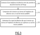
- the monitoring device 20 compares the voltage V D across the terminals of the detection impedance 45 with the predefined voltage threshold S. This comparison of the voltage V D with the predefined voltage threshold S is carried out in particular by the detection module 50, and typically via the crossing detection stage 90.
- This sudden change in the voltage V D across the terminals of the detection impedance 45 is visible on the figure 5 where a curve 215 represents the temporal evolution of said voltage V D .
- This curve 215 then shows several voltage peaks 218 corresponding to the appearance of the short-circuit in the converter 10, and in particular in at least one of the switching branches 40. These voltage peaks 218 mark the start of operation in short-circuit condition of converter 10, represented by arrow M2, following normal operation of converter 10 represented by arrow M1.
- the monitoring method then goes on to the next step 220 during which the monitoring device 20 generates the detection signal in order to indicate that the voltage V D at the terminals of the detection impedance 45 is greater than the predefined voltage threshold S, and that a short-circuit has then probably appeared in the converter 10.
- This generation of the detection signal is carried out by the detection module 50, and in particular by the generation stage 94, such as the optocoupler 138.
- the detection by the detection module 50 is then particularly effective and reactive, since the detection module 50 generates the detection signal in a time lapse ⁇ t of the order of 60 ns, as represented on the figure 6 where the instant of triggering of the optocoupler 138 represented by the arrow E takes place approximately 60 ns after the appearance of the short circuit.
- the curve 300 represents the current flowing through the optocoupler 138
- the curve 310 represents a voltage generated simulating a short circuit in order to validate the detection module 50
- the curve 320 represents a triggering threshold of the optocoupler 138, substantially equal to 2mA.
- the instant of triggering of the optocoupler 138 is slightly offset in time with respect to the intersection of the curve 300 (representing the current through the optocoupler 138) with the cut 320 (representing the triggering threshold of this optocoupler), and this slight time shift (of the order of 10 ns) is due to a propagation time inside the optocoupler 138 itself.
- the duration during which the short-circuit voltage is greater than the voltage threshold S is relatively small, of the order of 100 ns (between time instants 30 ns and 130 ns), which makes it possible to avoid untimely triggering of short-circuit detection, that is to say false alarms .
- the optocoupler 138 After detection of the short-circuit, the optocoupler 138 has enough time to generate the detection signal, since this generation is possible from the triggering of the optocoupler 138 represented by the arrow E and as long as the current crossing the optocoupler 138 is above the trigger threshold, that is to say for more than 150 ns (between the time instants 60 ns and 225 ns).
- the value of the sense impedance 45 typically depends on the material from which the switching semiconductor components 66 are made.
- the value of the inductance is of the order of a few tens of nH if the material of the semiconductor switching component 66 is gallium nitride (GaN), and of the order of a hundred nH if the material of the semiconductor switching component 66 is silicon carbide (SiC) or silicon (Si).
- the switching time of the semiconductor switching component 66 is much shorter when said switching component 66 is made of gallium nitride, the switching time then being typically of the order of 10 ns, than when said switching component 66 is made of silicon carbide or silicon, the switching time then being of the order of 50 to 100 ns, this which implies a 5 to 10 times higher sense inductance.
- the detection impedance 45 is an inductance
- the voltage V D across the terminals of said inductance is in L.di/dt where L is the value of the detection inductance, and di/dt represents the time derivative of the current, i.e. its variation over time.
- the time delta dt therefore corresponds substantially to the switching time of the semiconductor switching component 66, and the person skilled in the art will then observe that the faster said switching component 66 , the higher the voltage V D at the terminals of the detection impedance 45 will be for the same impedance value. It is therefore preferable to vary the value of the impedance according to the material of the switching component 66, in order to have approximately the same voltage across the terminals of the detection impedance 45 of a switching component technology 66 to another, and in particular to have substantially the same predefined detection threshold S regardless of the material of the semiconductor switching component 66.
- the monitoring device 20 and the monitoring method according to the invention make it possible to quickly detect the appearance of a short-circuit in one of the switching branches 40 of the converter 10, since the securing of the converter 10 requires approximately 100 to 200 ns from the appearance of the short-circuit, the duration between the 60 ns required for the detection of the short-circuit by the detection module 50 and the setting in safety corresponding to the duration of generation of the signal by the generation stage 94, such as the optical signal generation time by the optocoupler 138, followed by the information processing time by a microcontroller receiving said optical signal, and finally the control time of the switches 64 of the converter 10 in the open position for the safety of said converter.
- the switches 64 comprise semiconductor switching components 66 made of galium nitride since the short-circuit withstand time of the semiconductor component switching conductor 66 is of the order of 1 ⁇ s when the switching component 66 is made of gallium nitride, and of the order of 10 ⁇ s when the latter is made of silicon, and of the order of 100 to 200 ⁇ s when it is made of silicon carbide.
- This difference in short-circuit withstand depending on the material of the semiconductor switching component 66 is linked to the energy withstand, in adiabatic conditions, of such components.
- the energy resistance is of the order of 10 to 20 J/cm 2 for silicon carbide, of the order of 1 J/cm 2 for silicon, and of the order of 0.1 J/ cm 2 for gallium nitride.
- the capacitance of the capacitor 56 in particular that of the second filtering branch 38 closest to the switching branches 40, is dimensioned so that the short-circuited switches 64 hold the discharge energy of the corresponding filter branch 36, 38, in particular of the second filter branch 38.
- the capacitance C of capacitor 56 must be less, preferably much less, than 1.25 ⁇ F.
- the monitoring device 20 and the monitoring method according to the invention then make it possible to carry out a very rapid detection of the appearance of a short-circuit in the converter 10, while not disturbing the operation of the converter 10 in operating mode. nominal, when it is operating normally.
- the monitoring device 20 and the monitoring method according to the invention allow improved monitoring of the converter 10, in particular when the converter 10 comprises switches 64 made of broadband semiconductor material.
Landscapes
- Engineering & Computer Science (AREA)
- Power Engineering (AREA)
- Physics & Mathematics (AREA)
- General Physics & Mathematics (AREA)
- Microelectronics & Electronic Packaging (AREA)
- Ceramic Engineering (AREA)
- Condensed Matter Physics & Semiconductors (AREA)
- Computer Hardware Design (AREA)
- Manufacturing & Machinery (AREA)
- Power Conversion In General (AREA)
- Measurement Of Current Or Voltage (AREA)
- Dc-Dc Converters (AREA)
Applications Claiming Priority (1)
| Application Number | Priority Date | Filing Date | Title |
|---|---|---|---|
| FR2113576A FR3130385B1 (fr) | 2021-12-15 | 2021-12-15 | Dispositif et procédé de surveillance d’un convertisseur d’énergie électrique, système de conversion d’énergie électrique associé |
Publications (1)
| Publication Number | Publication Date |
|---|---|
| EP4199345A1 true EP4199345A1 (de) | 2023-06-21 |
Family
ID=80736109
Family Applications (1)
| Application Number | Title | Priority Date | Filing Date |
|---|---|---|---|
| EP22213560.0A Pending EP4199345A1 (de) | 2021-12-15 | 2022-12-14 | Vorrichtung und verfahren zur überwachung eines elektrischen energiewandlers, zugehöriges elektrisches energieumwandlungssystem |
Country Status (3)
| Country | Link |
|---|---|
| US (1) | US20230188041A1 (de) |
| EP (1) | EP4199345A1 (de) |
| FR (1) | FR3130385B1 (de) |
Citations (3)
| Publication number | Priority date | Publication date | Assignee | Title |
|---|---|---|---|---|
| EP2899886A1 (de) * | 2014-01-22 | 2015-07-29 | Hitachi, Ltd. | Halbleiterantriebsvorrichtung und Spannungsumwandlungsvorrichtung damit |
| US10158291B1 (en) * | 2015-11-17 | 2018-12-18 | Bel Power Solutions Inc. | DC/DC converter for high voltage applications with input voltage boost, input capacitor discharge and output capacitor compensation modes |
| US20190146020A1 (en) * | 2017-11-13 | 2019-05-16 | Texas Instruments Incorporated | Fully differential current sensing |
-
2021
- 2021-12-15 FR FR2113576A patent/FR3130385B1/fr active Active
-
2022
- 2022-12-13 US US18/065,326 patent/US20230188041A1/en active Pending
- 2022-12-14 EP EP22213560.0A patent/EP4199345A1/de active Pending
Patent Citations (3)
| Publication number | Priority date | Publication date | Assignee | Title |
|---|---|---|---|---|
| EP2899886A1 (de) * | 2014-01-22 | 2015-07-29 | Hitachi, Ltd. | Halbleiterantriebsvorrichtung und Spannungsumwandlungsvorrichtung damit |
| US10158291B1 (en) * | 2015-11-17 | 2018-12-18 | Bel Power Solutions Inc. | DC/DC converter for high voltage applications with input voltage boost, input capacitor discharge and output capacitor compensation modes |
| US20190146020A1 (en) * | 2017-11-13 | 2019-05-16 | Texas Instruments Incorporated | Fully differential current sensing |
Non-Patent Citations (5)
| Title |
|---|
| J. PERSON, SHORT CIRCUIT DETECTION METHODS FOR SILICON CARBIDE (SIC) POWER SEMICONDUCTORS |
| LAUMEN MICHAEL ET AL: "Ultra-Fast Short-Circuit Detection for SiC-MOSFETs Using DC-Link Voltage Monitoring", 2020 IEEE 11TH INTERNATIONAL SYMPOSIUM ON POWER ELECTRONICS FOR DISTRIBUTED GENERATION SYSTEMS (PEDG), IEEE, 28 September 2020 (2020-09-28), pages 547 - 553, XP033854241, DOI: 10.1109/PEDG48541.2020.9244367 * |
| OINONEN MARKUS ET AL: "Current measurement and short-circuit protection of an IGBT based on module parasitics", 2014 16TH EUROPEAN CONFERENCE ON POWER ELECTRONICS AND APPLICATIONS, IEEE, 26 August 2014 (2014-08-26), pages 1 - 9, XP032651268, DOI: 10.1109/EPE.2014.6910824 * |
| PERSON JONAS ET AL: "Short Circuit Detection Methods for Silicon Carbide (SiC) Power Semiconductors", PCIM EUROPE 2019, 9 May 2019 (2019-05-09), pages 217 - 223, XP055946816, ISBN: 978-3-8007-4938-6, Retrieved from the Internet <URL:https://ieeexplore.ieee.org/stampPDF/getPDF.jsp?tp=&arnumber=8767500&ref=aHR0cHM6Ly93d3cuZ29vZ2xlLmNvbS8=> [retrieved on 20220727] * |
| S. HAIN, NEW ULTRA FAST SHORT CIRCUIT DETECTION METHOD WITHOUT USING THE DESATURATION PROCESS OF THE POWER SEMICONDUCTOR |
Also Published As
| Publication number | Publication date |
|---|---|
| FR3130385B1 (fr) | 2023-11-24 |
| US20230188041A1 (en) | 2023-06-15 |
| FR3130385A1 (fr) | 2023-06-16 |
Similar Documents
| Publication | Publication Date | Title |
|---|---|---|
| EP2122432B1 (de) | Spannungsbegrenzer und schutz für ein fotovoltaisches modul | |
| EP1950885B1 (de) | Steuervorrichtung eines elektronischen Leistungstrenners und eine solche Vorrichtung umfassender Stromrichter | |
| EP0579561A1 (de) | Schutzschaltung gegen Überspannungen for Leistungsbauteil | |
| FR2945900A1 (fr) | Convertisseur de puissance utilisant un redresseur a transistors normalement fermes. | |
| FR3004019A1 (fr) | Composant de protection contre des surtensions | |
| FR2863115A1 (fr) | Interrupteur de circuit en cas de defaut a la terre. | |
| EP2747271B1 (de) | Schutzvorrichtung gegen Überlaststrom mindestens eines elektronischen Schaltzweiges, Stromumwandlungssystem, das eine solche Schutzvorrichtung umfasst, und entsprechendes Steuerverfahren | |
| FR3012696A1 (fr) | Circuit de protection contre des surtensions | |
| EP3070798B1 (de) | Schutzvorrichtung gegen überspannungen | |
| EP0677907B1 (de) | Überstromschutzvorrichtung | |
| FR2898441A1 (fr) | Procede de parametrage d'un convertisseur et convertisseur mettant en oeuvre le procede | |
| EP1992069B1 (de) | Einrichtung zur steuerung eines mos-transistors | |
| FR2475825A1 (fr) | Dispositif electronique de commutation a effet de proximite, protege contee les impulsions parasites | |
| FR2572600A1 (fr) | Stabilisateur electronique de tension, utilisable en particulier dans l'automobile, avec protection contre les surtensions transitoires de polarite opposee a celle du generateur | |
| FR2923331B1 (fr) | Appareil electrique rotatif pour automobile | |
| EP2756592B1 (de) | Verfahren zum steuern eines gesteuerten schalters der die versorgung eines elektrischen motors schaltet | |
| EP4199345A1 (de) | Vorrichtung und verfahren zur überwachung eines elektrischen energiewandlers, zugehöriges elektrisches energieumwandlungssystem | |
| EP2209211B1 (de) | Statischer Hochspannungsschalter | |
| EP0688151A1 (de) | Anordnung zum Steuern einer Niederdruckleuchtstofflampe | |
| FR2535551A1 (fr) | Dispositif de commutation electronique a faible dissipation de puissance | |
| EP3938793B1 (de) | Elektrische anlage mit einem überwachungsmodul | |
| WO2024132545A1 (fr) | Installation solaire a panneau photovoltaique | |
| EP0141698B1 (de) | Stromdetektorschaltung mit niedrigem Leistungsverbrauch und Steuerschaltung einer mit ihr bestückten elektronischen Anordnung | |
| EP3523867B1 (de) | Schaltung zum entladen eines elektrischen hochspannungssystems | |
| EP4387079A1 (de) | Steuerungssystem für einen spannungswandler |
Legal Events
| Date | Code | Title | Description |
|---|---|---|---|
| PUAI | Public reference made under article 153(3) epc to a published international application that has entered the european phase |
Free format text: ORIGINAL CODE: 0009012 |
|
| STAA | Information on the status of an ep patent application or granted ep patent |
Free format text: STATUS: REQUEST FOR EXAMINATION WAS MADE |
|
| 17P | Request for examination filed |
Effective date: 20221214 |
|
| AK | Designated contracting states |
Kind code of ref document: A1 Designated state(s): AL AT BE BG CH CY CZ DE DK EE ES FI FR GB GR HR HU IE IS IT LI LT LU LV MC ME MK MT NL NO PL PT RO RS SE SI SK SM TR |