EP0188208B2 - Kammer für Plasma-Behandlung - Google Patents
Kammer für Plasma-Behandlung Download PDFInfo
- Publication number
- EP0188208B2 EP0188208B2 EP19860100109 EP86100109A EP0188208B2 EP 0188208 B2 EP0188208 B2 EP 0188208B2 EP 19860100109 EP19860100109 EP 19860100109 EP 86100109 A EP86100109 A EP 86100109A EP 0188208 B2 EP0188208 B2 EP 0188208B2
- Authority
- EP
- European Patent Office
- Prior art keywords
- substrates
- chamber
- electrodes
- plasma
- transport track
- Prior art date
- Legal status (The legal status is an assumption and is not a legal conclusion. Google has not performed a legal analysis and makes no representation as to the accuracy of the status listed.)
- Expired - Lifetime
Links
- 239000000758 substrate Substances 0.000 claims description 79
- 238000012545 processing Methods 0.000 claims description 28
- 230000005684 electric field Effects 0.000 claims description 14
- 239000000376 reactant Substances 0.000 claims description 6
- 239000007789 gas Substances 0.000 description 54
- 238000000034 method Methods 0.000 description 18
- 230000008569 process Effects 0.000 description 16
- 238000005530 etching Methods 0.000 description 9
- 238000000151 deposition Methods 0.000 description 8
- 230000008021 deposition Effects 0.000 description 8
- 238000005192 partition Methods 0.000 description 8
- XKRFYHLGVUSROY-UHFFFAOYSA-N Argon Chemical compound [Ar] XKRFYHLGVUSROY-UHFFFAOYSA-N 0.000 description 6
- 238000000429 assembly Methods 0.000 description 5
- 230000000712 assembly Effects 0.000 description 5
- 238000009832 plasma treatment Methods 0.000 description 5
- 238000004544 sputter deposition Methods 0.000 description 5
- QGZKDVFQNNGYKY-UHFFFAOYSA-N Ammonia Chemical compound N QGZKDVFQNNGYKY-UHFFFAOYSA-N 0.000 description 4
- QVGXLLKOCUKJST-UHFFFAOYSA-N atomic oxygen Chemical compound [O] QVGXLLKOCUKJST-UHFFFAOYSA-N 0.000 description 4
- 238000004140 cleaning Methods 0.000 description 4
- 238000009826 distribution Methods 0.000 description 4
- 238000002955 isolation Methods 0.000 description 4
- 238000011068 loading method Methods 0.000 description 4
- 239000000203 mixture Substances 0.000 description 4
- 239000001301 oxygen Substances 0.000 description 4
- 229910052760 oxygen Inorganic materials 0.000 description 4
- 238000010587 phase diagram Methods 0.000 description 4
- RYGMFSIKBFXOCR-UHFFFAOYSA-N Copper Chemical compound [Cu] RYGMFSIKBFXOCR-UHFFFAOYSA-N 0.000 description 3
- 229910052786 argon Inorganic materials 0.000 description 3
- 229910052802 copper Inorganic materials 0.000 description 3
- 239000010949 copper Substances 0.000 description 3
- 230000007246 mechanism Effects 0.000 description 3
- 238000001020 plasma etching Methods 0.000 description 3
- 238000005086 pumping Methods 0.000 description 3
- KDLHZDBZIXYQEI-UHFFFAOYSA-N Palladium Chemical compound [Pd] KDLHZDBZIXYQEI-UHFFFAOYSA-N 0.000 description 2
- 239000004809 Teflon Substances 0.000 description 2
- 229920006362 Teflon® Polymers 0.000 description 2
- 230000008901 benefit Effects 0.000 description 2
- 238000006243 chemical reaction Methods 0.000 description 2
- 239000011248 coating agent Substances 0.000 description 2
- 238000000576 coating method Methods 0.000 description 2
- 239000004020 conductor Substances 0.000 description 2
- 238000011109 contamination Methods 0.000 description 2
- 239000000463 material Substances 0.000 description 2
- 238000012986 modification Methods 0.000 description 2
- 230000004048 modification Effects 0.000 description 2
- 239000012811 non-conductive material Substances 0.000 description 2
- 238000010899 nucleation Methods 0.000 description 2
- 239000013077 target material Substances 0.000 description 2
- 239000004593 Epoxy Substances 0.000 description 1
- 150000001412 amines Chemical class 0.000 description 1
- 229910021529 ammonia Inorganic materials 0.000 description 1
- 230000002457 bidirectional effect Effects 0.000 description 1
- 239000003990 capacitor Substances 0.000 description 1
- 239000000919 ceramic Substances 0.000 description 1
- 238000004891 communication Methods 0.000 description 1
- 238000007796 conventional method Methods 0.000 description 1
- 238000009792 diffusion process Methods 0.000 description 1
- 239000006185 dispersion Substances 0.000 description 1
- 230000000694 effects Effects 0.000 description 1
- 238000000454 electroless metal deposition Methods 0.000 description 1
- 238000009713 electroplating Methods 0.000 description 1
- 238000005516 engineering process Methods 0.000 description 1
- 230000005284 excitation Effects 0.000 description 1
- 239000010408 film Substances 0.000 description 1
- 238000007667 floating Methods 0.000 description 1
- 238000003682 fluorination reaction Methods 0.000 description 1
- 239000011521 glass Substances 0.000 description 1
- 238000010438 heat treatment Methods 0.000 description 1
- 239000011261 inert gas Substances 0.000 description 1
- 150000002500 ions Chemical class 0.000 description 1
- 238000004519 manufacturing process Methods 0.000 description 1
- 239000011159 matrix material Substances 0.000 description 1
- 238000001465 metallisation Methods 0.000 description 1
- 230000007935 neutral effect Effects 0.000 description 1
- 229910000069 nitrogen hydride Inorganic materials 0.000 description 1
- 238000010943 off-gassing Methods 0.000 description 1
- 229910052763 palladium Inorganic materials 0.000 description 1
- 229920000642 polymer Polymers 0.000 description 1
- 239000010970 precious metal Substances 0.000 description 1
- 238000002360 preparation method Methods 0.000 description 1
- 239000007787 solid Substances 0.000 description 1
- TXEYQDLBPFQVAA-UHFFFAOYSA-N tetrafluoromethane Chemical compound FC(F)(F)F TXEYQDLBPFQVAA-UHFFFAOYSA-N 0.000 description 1
- 239000010409 thin film Substances 0.000 description 1
- 238000012546 transfer Methods 0.000 description 1
- 238000009489 vacuum treatment Methods 0.000 description 1
- 235000012431 wafers Nutrition 0.000 description 1
Images



Classifications
-
- C—CHEMISTRY; METALLURGY
- C23—COATING METALLIC MATERIAL; COATING MATERIAL WITH METALLIC MATERIAL; CHEMICAL SURFACE TREATMENT; DIFFUSION TREATMENT OF METALLIC MATERIAL; COATING BY VACUUM EVAPORATION, BY SPUTTERING, BY ION IMPLANTATION OR BY CHEMICAL VAPOUR DEPOSITION, IN GENERAL; INHIBITING CORROSION OF METALLIC MATERIAL OR INCRUSTATION IN GENERAL
- C23C—COATING METALLIC MATERIAL; COATING MATERIAL WITH METALLIC MATERIAL; SURFACE TREATMENT OF METALLIC MATERIAL BY DIFFUSION INTO THE SURFACE, BY CHEMICAL CONVERSION OR SUBSTITUTION; COATING BY VACUUM EVAPORATION, BY SPUTTERING, BY ION IMPLANTATION OR BY CHEMICAL VAPOUR DEPOSITION, IN GENERAL
- C23C16/00—Chemical coating by decomposition of gaseous compounds, without leaving reaction products of surface material in the coating, i.e. chemical vapour deposition [CVD] processes
- C23C16/44—Chemical coating by decomposition of gaseous compounds, without leaving reaction products of surface material in the coating, i.e. chemical vapour deposition [CVD] processes characterised by the method of coating
- C23C16/54—Apparatus specially adapted for continuous coating
-
- C—CHEMISTRY; METALLURGY
- C23—COATING METALLIC MATERIAL; COATING MATERIAL WITH METALLIC MATERIAL; CHEMICAL SURFACE TREATMENT; DIFFUSION TREATMENT OF METALLIC MATERIAL; COATING BY VACUUM EVAPORATION, BY SPUTTERING, BY ION IMPLANTATION OR BY CHEMICAL VAPOUR DEPOSITION, IN GENERAL; INHIBITING CORROSION OF METALLIC MATERIAL OR INCRUSTATION IN GENERAL
- C23C—COATING METALLIC MATERIAL; COATING MATERIAL WITH METALLIC MATERIAL; SURFACE TREATMENT OF METALLIC MATERIAL BY DIFFUSION INTO THE SURFACE, BY CHEMICAL CONVERSION OR SUBSTITUTION; COATING BY VACUUM EVAPORATION, BY SPUTTERING, BY ION IMPLANTATION OR BY CHEMICAL VAPOUR DEPOSITION, IN GENERAL
- C23C14/00—Coating by vacuum evaporation, by sputtering or by ion implantation of the coating forming material
- C23C14/22—Coating by vacuum evaporation, by sputtering or by ion implantation of the coating forming material characterised by the process of coating
- C23C14/56—Apparatus specially adapted for continuous coating; Arrangements for maintaining the vacuum, e.g. vacuum locks
-
- H—ELECTRICITY
- H05—ELECTRIC TECHNIQUES NOT OTHERWISE PROVIDED FOR
- H05K—PRINTED CIRCUITS; CASINGS OR CONSTRUCTIONAL DETAILS OF ELECTRIC APPARATUS; MANUFACTURE OF ASSEMBLAGES OF ELECTRICAL COMPONENTS
- H05K3/00—Apparatus or processes for manufacturing printed circuits
- H05K3/0011—Working of insulating substrates or insulating layers
- H05K3/0055—After-treatment, e.g. cleaning or desmearing of holes
-
- H—ELECTRICITY
- H05—ELECTRIC TECHNIQUES NOT OTHERWISE PROVIDED FOR
- H05K—PRINTED CIRCUITS; CASINGS OR CONSTRUCTIONAL DETAILS OF ELECTRIC APPARATUS; MANUFACTURE OF ASSEMBLAGES OF ELECTRICAL COMPONENTS
- H05K2203/00—Indexing scheme relating to apparatus or processes for manufacturing printed circuits covered by H05K3/00
- H05K2203/09—Treatments involving charged particles
- H05K2203/095—Plasma, e.g. for treating a substrate to improve adhesion with a conductor or for cleaning holes
Definitions
- the invention relates to a plasma reactor chamber for continuous plasma processing of the major surfaces of a plurality of substrates.
- the chamber is particularly well suited for plasma processing of printed circuit boards or cards having through-holes or viaduct holes. commonly called vias. Among others.
- the chamber permits plasma etching and cleaning processes.
- an atom may be displaced from the surface of a target connected to a cathode by a process called sputtering or sputter deposition.
- the target is most often constructed of electrically conductive material such as copper or the like.
- the cathode to which the target is attached is subjected to a relatively high voltage, either DC or radio frequency, in an inert atmosphere such as argon.
- the inert gas is ionized, forming an excited gaseous state (plasma) from which positive ions escape to bombard the exposed surface of the target.
- Through holes or viaduct holes are paths for electrical interconnections between a first-level conductive pattern and a second- or higher-level conductive pattern.
- precious metal e.g., palladium
- electroless metal deposition have been used to coat the walls of the vias, often followed by electroplating.
- plasma technology has been applied to this problem.
- nonuniformity of a plasma field can result in nonuniform etching, nonuniform depostion and/ or nonuniform cleaning of via holes and through holes, the latter being referred to as desmearing.
- etching process for example, a more intense plasma field in the center of a board results in a higher etching rate for that portion of the board, whereas a relatively sparse plasma density at the edges of the board results in a proportionally and predictably low etch rate for those sections. It has been found that nonuniformity of an electric field in proximity to an electrically floating printed circuit board results in nonuniform plasma treatment thereof.
- One conventional method for attaining more uniform plasma etch results requires a high CF4 concentration to produce fluorination where desired to decrease etch rate.
- oppositely charged electrodes are provided in a vacuum chamber to initiate a plasma reaction.
- a vacuum chamber to initiate a plasma reaction.
- Such apparatus is shown, for example, in European patent application, No. 85.101920.8, filed on February 22, 1985, and assigned to the present assignee.
- Such an apparatus as disclosed, can be used only in batch operations to treat only one major surface of a substrate at a time, as opposed to continuous or semi-continuous operations. Moreover, since much of the reactant gases is consumed, the uniformity of plasma deposition is ensured only for relatively small substrates or wafers. Finally, the apparatus is intended to be used for plasma deposition, only not etching.
- U.S. Patent No. 4,264,393 issued to Gorin, et al discloses a reactor apparatus for plasma etching or deposition.
- the apparatus has two parallel plates within the reactor, one of which functions as manifold for reactant gases which are dispensed through a regular array of orifices into the r.f. field between the plates.
- the parallel plate structure can be stacked in an array of alternating grounded and r.f. plates to increase the apparatus capacity.
- the reactant gases are introduced only from one direction (i.e., the plates have an array of orifices only on one side), resulting in one-sided etching of substrates or via holes therein.
- JP Patent A-59-70766 discloses a vacuum plasma system for processing of cylindrical substrates.
- a charging chamber a number of substrates are mounted on a carrier which is then transferred to a vacuum treatment chamber.
- semicylindrical electrodes are moved forward to individually enclose the substrates. After plasma treatment, the electrodes are moved back and the carrier with the subtrates is removed from the treatment chamber.
- a system for plasma processing the major surfaces of a plurality of substrates comprising a plasma reactor chamber, provision for continously introducing a gas to be converted in a reactive species by an electrical field, provision for applying such electric fields to the substrates by operatively connecting a first RF power source to a first electrode, being disposed on one side of said substrates, and a second RF power source to a second electrode opposite to said first electrode, provision for continuously exhausting gas, an automatic transport or drive mechanism connected to the chamber and the substrates to facilitate the advancement of substrates seriatim along a predetermined path in the chamber, and a vacuum lock connected to the chamber for maintaining a substantially constant atmosphere in the chamber while each of the substrates is inserted into and removed from the chamber.
- the plasma reactor chamber permits continuous or semi-continuous processing of a plurality of substrates as compared to the hitherto used batch processing systems, and it provides for uniform processing of both sides of the substrates as well as of the via holes that may be present in the substrates.
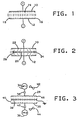
- FIGURE 1 there is shown a cross sectional view of a conventional upper panel electrode 10 and a lower panel electrode 12, as is well known in the prior art. Both electrodes 10 and 12 have major axes parallel to one another. This configuration is referred to as parallel plate panel electrodes.
- a power supply is connected to each of these electrodes 10 and 12.
- a positive charge is applied to the upper electrode 10 and a negative charge is applied to the lower electrode 12, as shown in FIGURE 1 at a given instant of time.
- the electrical field between parallel electrodes 10 and 12, identified by reference numeral 14, is substantially uniform in the center region.
- the electrical field is more intense at both edges of the electrodes 10 and 12, however, as shown by reference numerals 16 and 18, respectively. Accordingly, neither the electrical field 14 nor the resulting plasma, not shown, is uniform at all locations proximate the electrodes 10 and 12.
- FIGURE 2 there is shown a cross sectional view of the same parallel plate panel electrodes 10 and 12 with a substrate 20 therebetween.
- the substrate 20 has a major axis substantially parallel to the major axis of the electrodes 10 and 12.
- the electrical field at a given instant of time has relatively low intensity in the center region 22 proximate the electrodes 10 and 12 and relatively high intensity at the outer edge regions 24 and 26 proximate the electrodes 10 and 12. It can be seen that conventional parallel plate panel electrodes 10 and 12 with a substrate 20 intermediate them results in a nonuniform electrical field.
- FIGURE 3 there is shown a plasma reactor system having an upper electrode 28 and a lower electrode 30 parallel thereto. Intermediate these two electrodes 28 and 30 and substantially parallel thereto, is a substrate 32 which is grounded or maintained at zero electrical potential.
- An r.f. source of power or generator 34 such as Model No. PM 145 manufactured by the Branson IPC Co., is electrically connected to the upper electrode 28.
- a second r.f. source of power 36 is electrically connected to the lower electrode 30.
- an impedance matching network 38 is connected to the upper r.f. power source 34 in series with the upper electrode 28.
- the impedance matching network includes fixed and variable capacitors.
- a second impedance matching network 40 is connected to the second r.f. power source 36 in series with the lower electrode 30.
- Alternating current phase diagrams 42 and 44 indicate the phase differential between r.f. power sources 34 and 36. It can be seen that the r.f. power sources 34 and 36 are 180° out of phase with one another at all times. It can also be seen that the electrical field generated between the upper and lower electrodes 28 and 30, respectively, is substantially uniform along the length of the substrate 32, including the end portions 46 and 48 thereof.
- FIGURE 4 there is shown a reactor chamber 50, which is designed for batch processing rather than continuous processing, and which is suited for maintaining a high vacuum for use in plasma processes.
- a reactor chamber 50 can be obtained from the Branson IPC Co., for example, as Model No. 7415.
- the chamber 50 is evacuated and then argon and oxygen or CF4 and oxygen are introduced thereto.
- a housing 52 is disposed within the reactor chamber 50.
- the housing 52 are mounted a plurality of cards or boards 54 suitable for having electrical circuits printed thereon.
- the boards 54 are electrically connected to one another by means of a bus structure 56 which, in turn, is grounded 57.
- Electrodes 58 and 60 are placed alternately on either side of the substrate 54. Electrodes 58 are electrically connected to one another by means of a bus structure 62.
- the bus structure 62 is electrically connected to an r.f. power generator 64 which is adapted, in the preferred embodiment, to operate at 13.5 MHz.
- an r.f. power generator 64 operating at a much lower frequency (e.g., 50 KHz) prevents creation of polymer species from feed gas.
- U.S. Patent No. 4,425,210 issued to Fazlin discloses relatively low frequency r.f. values. Thus the ionic plasma species etchants respond to the r.f. field to reach the through hole interior, providing uniform etch thereof.
- Phase diagram 65 represents the phase of the r.f. generator 64 at a given moment of time.
- Bus structure 66 is electrically isolated from, although physically supported by, bus structure 56 by means of insulating members 66a and 66b.
- This second bus structure 66 is electrically connected to a second r.f. power generator 68 also adapted to operate at 13.5 MHz.
- Phase diagram 69 represents the phase of second r.f. generator 68.
- the electrical signal from the first r.f. generator 64 is 180° out of phase with the electrical signal generated by the second r.f. generator 68 in the preferred embodiment.
- a comparison of AC phase diagrams 65 and 69 indicates this phase differential relationship.
- phase differential between the r.f. power generators 64 and 68 results in a more uniform electric field than can be obtained either by a single r.f. power generator or by a plurality of r.f. generators, all being in phase with one another.
- the phase differential need not be 180°.
- any phase differential between r.f. power generators 64 and 68 is within the scope of the present invention.
- Gas inlet and gas outlet pipes or tubes are connected to the reactor chamber 50 to introduce gas thereto or to remove gas therefrom as required.
- continuous gas introduction and exhaust can be accomplished by one or more of such lines connected to the chamber 50.
- FIGURE 5 there is shown a hollow electrode plasma system.
- This hollow electrode plasma system is surrounded by a plasma chamber, not shown, the interior of which is covered and protected by nonconductive material such as Teflon material.
- Teflon is a registered trademark of E.I. duPont de Nemours Co.
- a first hollow electrode 70 has a plurality of holes 72 drilled or punched in one major surface thereof.
- the holes are shown in phantom in FIGURE 5.
- the holes 72 are also shown in a rectilinear, uniform matrix pattern in the preferred embodiment. But it should be understood that any pattern of holes 72 that ensures uniform gas distribution may be used.
- this first hollow electrode 70 In spaced apart relationship to this first hollow electrode 70 is a substrate 74, the major axis of which is parallel to the major axis of the electrode 70. Connected to the electrode 70 is an r.f. power supply 76. The substrate 74 is grounded.
- a second hollow electrode 78 Located adjacent and substantially parallel to the substrate 74 is a second hollow electrode 78 having a plurality of holes, not shown, drilled or punched through both major surfaces thereof.
- a second r.f. power supply 80 is electrically connected to this hollow electrode 78.
- another substrate 82 is positioned substantially parallel to the hollow electrode 78 and is also grounded.
- a third hollow electrode 84 is positioned substantially parallel to the substrate 82.
- This electrode 84 also has a plurality of holes, not shown, drilled or punched completely therethrough.
- Another r.f. power supply 86 is connected to this hollow electrode 84.
- Another substrate 88 is placed substantially parallel to the third hollow electrode 84 and is also grounded.
- a fourth hollow electrode 90 having holes, not shown, drilled or punched therethrough on one major surface only is placed substantially parallel to the substrate 88 and is, in turn, electrically connected to a last r.f. power supply 92.
- Gas inlet pipes 94, 96, 98 and 100 are connected to the hollow electrodes 70, 78, 84 and 90, respectively. Independently operable valves 94a, 96a, 98a and 100a are placed in corresponding inlet pipes 94, 96, 98 and 100 to shut off the flow of gas therethrough. Connected to the inlet pipes 94, 96, 98, 100 is an inlet manifold 101 for distributing gas evenly to the hollow electrodes 70, 78, 84, 90.
- gas outlet pipes On the side of the electrodes opposite the gas inlet manifold 101 are gas outlet pipes, one of which being 102, having independently operable valves 102a corresponding to each pipe.
- the gas outlet pipes associated with hollow electrodes 78, 84 and 90 are not shown in FIGURE 5. All of the gas outlet pipes are connected to their associated hollow electrodes and to an outlet manifold 104 for allowing gas to be exhausted from the hollow electrodes uniformly.
- a main gas feed line 106 is connected to the inlet manifold 101.
- a main gas exhaust line 108 is connected to the outlet manifold 104.
- gas inlet lines 106, 94, 96, 98, 100 and manifold 101 and the function of the gas outlet lines 108, 102 and manifold 104 can be reversed, if desired. That is, when appropriate, gas may be introduced by means of the main gas exhaust line 108 and exhausted by means of the main gas feed line 106.
- inlet and outlet pipes in direct conjunction with hollow electrodes maximizes gas distribution and flow across the substrates, thus ensuring uniformity of gas flow as well as uniformity of electric field.
- the advantage of these combined uniformities is a more accurate and uniform etching or deposition during the plasma process.
- valves 94a, 96a, 98a, 100a, 102a and those not shown should also be described for a clear understanding of the hollow electrode plasma system.
- valves 94a, 96a, 98a and 100a are placed in an open position to allow the gas to reach and enter the hollow electrodes 70, 78, 84 and 90 respectively.
- the outlet pipe valves 102a and others, not shown are placed in a closed position, the gas is forced through the hollow electrode holes 72.
- gas introduced into the hollow electrodes 70, 78, 84, 90 under pressure by means of the corresponding gas inlet ports 94, 96, 98, 100 is distributed through the electrode holes 72 to impinge on the substrates 74, 82, 88 in a substantially uniform manner.
- inlet valves 94a, 96a, 98a and 100a and outlet valves 102a and others can result in gas flowing through the hollow electrodes 70, 78, 84, 90 in any one of a number of gas flow patterns.
- Individual substrates or groups of substrates can be processed by appropriately setting the inlet and outlet valves and selecting the main gas feed line 106 and main gas exhaust line 108. It should also be understood that any number of hollow electrodes and alternating substrates may be used in accordance with this invention.
- the gas inlet lines 94, 96, 98 and 100 are used to introduce gas with which a plasma reaction may be maintained.
- gases are commonly CF4, O2, ammonia, freon and the like.
- a gas composition having a mixture of any of the aforementioned molecules can also be used.
- a mixture of argon and oxygen can be used with relatively low r.f. power generator frequencies to clean high aspect ratio through holes.
- the phase differential among r.f. power sources is as follows.
- R.f. power supplies 76 and 86 are in phase with one another.
- R.f. power supplies 80 and 92, while being in phase with one another, are 180° out of phase with the aforementioned r.f. power supply pair 76 and 86.
- Typical frequencies are in the range of 50 KHz to 13.5 MHz.
- FIGURE 6 there is shown a cross-sectional portion of hollow electrodes 70 and 78 and substrate 74 therebetween, taken along line 6-6 of FIGURE 5.
- the hollow electrode 70 has two walls: a left, solid wall 109 and a right wall 110 with holes 72.
- the holes 72 of the right wall 110 of electrode 70 are tapered in such a way as to allow a dispersion of gas from the left portion of the reactor chamber 50 (FIGURE 4) to the right portion thereof.
- the holes 72 in electrode 70 have a smaller diameter on the left side of wall 110 and a larger diameter on the right side of wall 110 of the electrode 70.
- the orientation of the tapered holes 72 is reversed on the left wall 112 of the hollow electrode 78 so as to allow uniform gas distribution to the rightmost major surface of the substrate 74. It should be understood that tapering of the holes 72 in the manner shown is useful for one substrate 74 shown in this example placed intermediate two hollow electrodes 70 and 78. Alternative arrangements and orientations of electrode holes 72 can easily be designed for modifications to the plasma process, depending on gas flow direction and number of substrates to be processed concurrently.
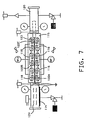
- FIGURE 7 there is shown a top view of a system adapted for use in a continuous plasma treatment process having uniform gas flow and uniform electric field.
- a vacuum lock 114 is connected to a linear reactor chamber 115.
- the vacuum lock 114 is used to permit substrates 122a, 122b, 122c or other articles to enter the reactor chamber 115 and move along a transport track 123 without affecting the atmosphere or vacuum therein.
- Electrodes 118 are disposed on the opposite side of the reactor centerline, each of which corresponding to one of the aforementioned electrodes 116.
- the electrodes 118 are electrically connected to a second r.f. power supply RF2 and are in phase with one another, but 180° out of phase with respect to electrodes 116.
- a second vacuum lock 120 is attached to the reactor chamber 115 on the side opposite the first vacuum lock 114. Vacuum lock 120 is used to remove substrates 122a, 122b, 122c from the reactor chamber 115 without affecting the atmosphere or vacuum therein.
- substrates 122a, 122b, 122c are shown in a vertical orientation. It should be understood that the orientation of the electrodes 116 and 118 may likewise be parallel to one another and horizontally disposed, similar to the schematic orientation shown in FIGURE 3.
- the substrates 122a, 122b, 122c are grounded in the preferred embodiment, but may be maintained at a fixed voltage potential throughout the plasma process.
- the substrates 122a, 122b, 122c are advanced along the transport track 123 from the initial vacuum lock 114 through the reactor chamber 115, between hollow electrodes 116 and 118 and through second vacuum lock 120.
- a drive mechanism not shown, advances each substrate on the transport track 123 linearly from one location in the reactor apparatus to another sequentially and continuously.
- Heating elements 124 disposed within the initial vacuum lock 114, can be used to preheat the substrates 122a, 122b, 122c before plasma etching or deposition occurs.
- the flow of gas through the hollow electrodes 116 and 118 and around and through the substrates 122a, 122b, 122c is shown in FIGURE 7 as arrowed lines.
- the hollow electrodes 116 and 118 have apertures on both sides as well as a series of holes forming a center sink intermediate the walls facing the substrates 122a, 122b, 122c.
- the reactor chamber 115 can be divided into two or more sections, each being isolated from one another and each being adapted to process substrates with a different gaseous composition.
- one or more secondary reactor chambers can be placed between the primary reactor chamber 115 and the vacuum lock 120 in each of which a different plasma process can be maintained, each independently from one another.
- Such a series of plasma treatment stages can be useful, for example, in etching, hole cleaning, board preparation and deposition or any combination of the above.
- FIGURE 8 there is shown a circular reactor chamber for continuous or semi-continuous plasma processing.
- the unit comprises essentially two cylindrical elements 130 and 132 at the upper and lower ends of which are secured upper and lower closure plate members, not shown in this top cross sectional view.
- the inner cylinder 132 which forms the vacuum manifold 134, provides for connecting into a central vacuum pump.
- radial partition assemblies such as 136 and 138, extending generally radially, divide the apparatus into a number of separate processing regions or chambers, such as 140 through 154, inclusive.
- These separate chambers are constructed so that a ring-like platform, not shown, may be suitably rotated within and through them to carry substrates.
- a conventional air lock or vacuum lock element 156 leads into one of the chambers 140 and provides for loading and unloading the substrates carried on the rotary ring platform.
- the control provides essentially a vacuum locking device which isolates the load and unload chamber 140 from all other portions of the unit. Isolation of the vacuum processing chambers 140 through 154 is achieved and effected by providing an extremely close tolerance between the substrate carrier platform and a differentially pumped isolation compartment 141.
- the carrier platform is arranged to pass from one chamber, such as 142 into an adjacent chamber 144, through openings provided in the walls of the radially extending partition assembly members 136 and 138. These openings are usually arranged in a rectangular form through the use of a series of right angled duct-like elements 158 to provide a controlled leakage path at both the top and the sides through which the platform moves.
- One side of the angled elements 158 is fastened to the partition wall 136, while the other side is free, except for the connection at the abutting edges which are welded or soldered to make a tight fit. This controlled leakage path provides efficient isolation of one process environment from another.
- the ring platform may be driven from any desired form of prime mover such as a motor and appropriate gears, not shown.
- the outer edge of the ring-like platform may be formed as a toothed member, for example, with the teeth adapted to mesh with the teeth of a driving pinion so that rotation is readily achieved.
- other forms of drives such as frictional members may be utilized.
- the apparatus described here is purely for convenience.
- the central vacuum manifold 134 is common to all of the formed chambers, 140 through 154.
- a valve element 180 of the generally butterfly type leads from each formed processing chamber into this central manifold 134.
- the specified processing chamber can be opened to the manifold 134 or can be closed off therefrom.
- a single high speed vacuum pumping system such as a diffusion or turbo pump, when connected to lead to vacuum manifold 134, can provide the necessary vacuum to all of the different formed processing chambers and radial partition assemblies.
- the pumping system can be further connected to various mechanical pumps for establishing desired vacuum level.
- Each of the separate valves 160 constitutes a controllably variable conductance element which is supported in the inner cylindrical wall. It is thus possible to have a multiplicity of differentially pumped processing chambers because of the radial partition assemblies separating each from the central vacuum manifold 134.
- the vacuum manifold communication to the radial partition assemblies between the separate chambers, such as 144 and 148, is provided by a fixed or controllable conductance entrance port 162 connected to corresponding isolation compartments between walls such as 136 and 138, so that the pressure therein is almost as low as that within the manifold 134 leading to the vacuum pump. Because of leakages and similar effects, this isolating region or compartment is usually at a slightly higher pressure than that of the vacuum manifold 134. The highest system pressure is, of course, found within such chambers as 140, 142, 144, 148, etc. It is these regions or compartments which constitute the various processing component volumes.
- the ring platform successively moves within the different processing chambers and, as. this occurs, the supported substrates which may be included within an appropriate atmosphere introduced in any appropriate and desired manner may be sputter treated by r.f. excitation of sputtering cathode elements 164 positioned within the various chambers or order vacuum processes. If desired, and in other that the relative pressures in the different chambers shall be separably controllable, it is apparent that each of the control mechanism conventionally represented for turning the valves 160 may be automatically operated.
- the directly pumped controlled leakage slots in the radial partition assembly 136, 138 eliminate process chamber contamination from one compartment to that adjacent to it.
- the substrate carrier platform In operation, the substrate carrier platform is confined to the vacuum environment. This reduces out-gassing.
- the directly pumped radial partition assemblies serve substantially to eliminate compartment contamination.
- a 4 ft. (121,92 cm) diameter circular processing chamber is approximately the equivalent of an 11 ft. (335,28 cm) length linear, in-line section.
- the circular processing system provides for substrate loading and unloading in adjacent areas. as contrasted with the in-line system which requires loading and unloading at opposite ends of the system, as previously described.
- the loading of substrates as well as the unloading thereof is achievable by any desired form of simple automatic method and permits a continuous or semi-continuous operation without causing the environment to vary. It is also readily controllable by computer control for different types of processing and purely automatic operation.
- circular reactor apparatus as well as the longitudinal reactor apparatus described in FIGURE 7, can be used with boards or substrates transported either vertically or horizontally.
- An oxygen plasma can be used in the continuous plasma device hereinabove described to improve adhesion between copper, the most commonly used electrical conductor, and epoxy, a nonconductive material. Moreover, a plasma consisting of NH3 and amine can be used to prepare a board for future seeding operations.
Landscapes
- Chemical & Material Sciences (AREA)
- Engineering & Computer Science (AREA)
- Chemical Kinetics & Catalysis (AREA)
- Materials Engineering (AREA)
- Mechanical Engineering (AREA)
- Metallurgy (AREA)
- Organic Chemistry (AREA)
- General Chemical & Material Sciences (AREA)
- Manufacturing & Machinery (AREA)
- Microelectronics & Electronic Packaging (AREA)
- Drying Of Semiconductors (AREA)
- ing And Chemical Polishing (AREA)
Claims (5)
- Plasma-Reaktionskammer (115) für die kontinuierliche Plasma-Behandlung der Hauptoberflächen einer Mehrzahl von Substraten (122A, 122B, 122C), umfassend:
eine Transportschiene (123) zum Halten der Substrate (122A, 122B, 122C);
Antriebsmittel zum reihenweisen Vorrücken der Substrate entlang der Transportschiene;
mit der Kammer (115) verbundene Vakuumschleusen (114, 120), über welche die Substrate (122A, 122B, 122C) in die Kammer eingeführt und aus der Kammer entnommen werden können, während eine im wesentlichen konstante Atmosphäre in der Kammer beibehalten wird;
eine Mehrzahl von im wesentlichen planaren, hohlen Elektrodenpaaren (116, 118), die entlang der Transportschiene (123) angeordnet sind, wobei die Elektroden jeden Paares im wesentlichen parallel einander gegenüberliegen und auf gegenüberliegenden Seiten der von der Transportschiene (123) gehaltenen Substrate angeordnet sind:
Mittel zum direkten und individuellen Einführen von reaktiven Gasen in die hohlen Elektroden, wodurch ein Gasstrom durch Öffnungen in den Wänden der Elektroden auf die Substrate gerichtet wird, und
Hochfrequenz-Generatoren zum Erzeugen elektrischer Felder, wobei ein erster derartiger Generator (RF1) operativ mit mindestens einer ersten der Elektroden (116), die auf einer Seite der von der Transportschiene (123) gehaltenen Substrate angeordnet sind, verbunden ist und ein zweiter derartiger Generator (RF2) operativ mit mindestens einer zweiten der Elektroden (118), die gegenüber zur ersten Elektrode (116) liegen, verbunden ist. - Kammer nach Anspruch 1, wobei die Antriebsmittel ein kontinuierliches Vorrücken der Substrate bewirken.
- Kammer nach Anspruch 1, wobei die Transportschiene (123) eine im wesentlichen geschlossene Schleife bildet.
- Kammer nach Anspruch 1, wobei der erste und zweite Generator (RF1, RF2) gegeneinander um 180° phasenverschoben sind.
- Kammer nach Anspruch 1, wobei die Substrate auf einem festen Spannungspotential gehalten werden.
Applications Claiming Priority (2)
| Application Number | Priority Date | Filing Date | Title |
|---|---|---|---|
| US69214485A | 1985-01-17 | 1985-01-17 | |
| US692144 | 1985-01-17 |
Publications (4)
| Publication Number | Publication Date |
|---|---|
| EP0188208A2 EP0188208A2 (de) | 1986-07-23 |
| EP0188208A3 EP0188208A3 (en) | 1987-09-30 |
| EP0188208B1 EP0188208B1 (de) | 1990-05-23 |
| EP0188208B2 true EP0188208B2 (de) | 1994-01-12 |
Family
ID=24779433
Family Applications (1)
| Application Number | Title | Priority Date | Filing Date |
|---|---|---|---|
| EP19860100109 Expired - Lifetime EP0188208B2 (de) | 1985-01-17 | 1986-01-07 | Kammer für Plasma-Behandlung |
Country Status (3)
| Country | Link |
|---|---|
| EP (1) | EP0188208B2 (de) |
| JP (1) | JPS61168922A (de) |
| DE (1) | DE3671482D1 (de) |
Cited By (1)
| Publication number | Priority date | Publication date | Assignee | Title |
|---|---|---|---|---|
| WO2005081592A1 (en) * | 2004-02-20 | 2005-09-01 | The University Of Sydney | An apparatus for plasma treatment |
Families Citing this family (12)
| Publication number | Priority date | Publication date | Assignee | Title |
|---|---|---|---|---|
| US5074456A (en) | 1990-09-18 | 1991-12-24 | Lam Research Corporation | Composite electrode for plasma processes |
| JP3215643B2 (ja) * | 1997-01-31 | 2001-10-09 | ワイエイシイ株式会社 | プラズマ処理装置 |
| US8770142B2 (en) | 2008-09-17 | 2014-07-08 | Veeco Ald Inc. | Electrode for generating plasma and plasma generator |
| US8851012B2 (en) | 2008-09-17 | 2014-10-07 | Veeco Ald Inc. | Vapor deposition reactor using plasma and method for forming thin film using the same |
| US8871628B2 (en) | 2009-01-21 | 2014-10-28 | Veeco Ald Inc. | Electrode structure, device comprising the same and method for forming electrode structure |
| US8257799B2 (en) | 2009-02-23 | 2012-09-04 | Synos Technology, Inc. | Method for forming thin film using radicals generated by plasma |
| US8758512B2 (en) | 2009-06-08 | 2014-06-24 | Veeco Ald Inc. | Vapor deposition reactor and method for forming thin film |
| US8771791B2 (en) | 2010-10-18 | 2014-07-08 | Veeco Ald Inc. | Deposition of layer using depositing apparatus with reciprocating susceptor |
| US20120114877A1 (en) * | 2010-11-05 | 2012-05-10 | Synos Technology, Inc. | Radical Reactor with Multiple Plasma Chambers |
| US8877300B2 (en) | 2011-02-16 | 2014-11-04 | Veeco Ald Inc. | Atomic layer deposition using radicals of gas mixture |
| US9163310B2 (en) | 2011-02-18 | 2015-10-20 | Veeco Ald Inc. | Enhanced deposition of layer on substrate using radicals |
| GB202312418D0 (en) * | 2023-08-14 | 2023-09-27 | P2I Ltd | Coating apparatus |
Family Cites Families (10)
| Publication number | Priority date | Publication date | Assignee | Title |
|---|---|---|---|---|
| US4013532A (en) | 1975-03-03 | 1977-03-22 | Airco, Inc. | Method for coating a substrate |
| JPS5291650A (en) * | 1976-01-29 | 1977-08-02 | Toshiba Corp | Continuous gas plasma etching apparatus |
| US4264393A (en) * | 1977-10-31 | 1981-04-28 | Motorola, Inc. | Reactor apparatus for plasma etching or deposition |
| JPS5571027A (en) * | 1978-11-24 | 1980-05-28 | Hitachi Ltd | Continuous surface treatment apparatus |
| JPS56152973A (en) * | 1980-04-30 | 1981-11-26 | Tokuda Seisakusho Ltd | Sputter etching device |
| US4289598A (en) * | 1980-05-03 | 1981-09-15 | Technics, Inc. | Plasma reactor and method therefor |
| US4282077A (en) * | 1980-07-03 | 1981-08-04 | General Dynamics, Pomona Division | Uniform plasma etching system |
| DE3107914A1 (de) | 1981-03-02 | 1982-09-16 | Leybold-Heraeus GmbH, 5000 Köln | Verfahren und vorrichtung zum beschichten von formteilen durch katodenzerstaeubung |
| JPS5970766A (ja) * | 1982-10-18 | 1984-04-21 | Ulvac Corp | プラズマcvd装置 |
| JPS59225524A (ja) * | 1983-06-06 | 1984-12-18 | Sanyo Electric Co Ltd | プラズマ反応方法 |
-
1985
- 1985-10-15 JP JP22793885A patent/JPS61168922A/ja active Granted
-
1986
- 1986-01-07 EP EP19860100109 patent/EP0188208B2/de not_active Expired - Lifetime
- 1986-01-07 DE DE8686100109T patent/DE3671482D1/de not_active Expired - Lifetime
Cited By (1)
| Publication number | Priority date | Publication date | Assignee | Title |
|---|---|---|---|---|
| WO2005081592A1 (en) * | 2004-02-20 | 2005-09-01 | The University Of Sydney | An apparatus for plasma treatment |
Also Published As
| Publication number | Publication date |
|---|---|
| DE3671482D1 (de) | 1990-06-28 |
| EP0188208A2 (de) | 1986-07-23 |
| JPS61168922A (ja) | 1986-07-30 |
| EP0188208B1 (de) | 1990-05-23 |
| JPH0439222B2 (de) | 1992-06-26 |
| EP0188208A3 (en) | 1987-09-30 |
Similar Documents
| Publication | Publication Date | Title |
|---|---|---|
| EP0188206B1 (de) | Einrichtung zur Erzeugung eines im wesentlichen homogenen Plasmas | |
| US5061359A (en) | Plasma processing apparatus including three bus structures | |
| EP0188207B1 (de) | Einrichtung zur Erzeugung einer homogenen Gasströmung in einer Plasma-Kammer | |
| EP0188208B2 (de) | Kammer für Plasma-Behandlung | |
| US4885074A (en) | Plasma reactor having segmented electrodes | |
| CA1128896A (en) | Treating multilayer printed wiring boards | |
| KR19990022867A (ko) | 고전류의 저에너지 이온 빔을 발생시키기 위한 개선된 평행이온 광학기 및 장치 | |
| US6168698B1 (en) | Apparatus for coating a substrate | |
| US4474659A (en) | Plated-through-hole method | |
| US5021138A (en) | Side source center sink plasma reactor | |
| US6216632B1 (en) | Plasma processing system | |
| JP2000200773A (ja) | 回路基板のプラズマ処理装置 | |
| US6390020B1 (en) | Dual face shower head magnetron, plasma generating apparatus and method of coating substrate | |
| EP0280074B1 (de) | Plasmareaktor | |
| JPH0237963A (ja) | 通電加熱部材 | |
| JPH1112742A (ja) | Cvd装置およびそのクリーニング方法 | |
| JP2993813B2 (ja) | プラズマcvd装置 | |
| JPS6126223A (ja) | エツチング方法および装置 | |
| JP2003086576A (ja) | 基板処理装置 | |
| JPH0955357A (ja) | 半導体製造装置および薄膜堆積方法 | |
| KR20000043924A (ko) | 플라즈마 증착 장비 및 이를 이용한 반도체 소자의 절연막형성 방법 | |
| MXPA00003218A (en) | Dual face shower head electrode for a magnetron plasma generating apparatus | |
| JPS63160394A (ja) | プリント回路板の製造方法 | |
| JPH01111871A (ja) | プラズマ気相成長装置 | |
| KR19980018389A (ko) | 다결정 다이아몬드의 플라즈마화학 분리 장치 |
Legal Events
| Date | Code | Title | Description |
|---|---|---|---|
| PUAI | Public reference made under article 153(3) epc to a published international application that has entered the european phase |
Free format text: ORIGINAL CODE: 0009012 |
|
| AK | Designated contracting states |
Kind code of ref document: A2 Designated state(s): DE FR GB |
|
| 17P | Request for examination filed |
Effective date: 19861125 |
|
| PUAL | Search report despatched |
Free format text: ORIGINAL CODE: 0009013 |
|
| AK | Designated contracting states |
Kind code of ref document: A3 Designated state(s): DE FR GB |
|
| 17Q | First examination report despatched |
Effective date: 19890202 |
|
| GRAA | (expected) grant |
Free format text: ORIGINAL CODE: 0009210 |
|
| AK | Designated contracting states |
Kind code of ref document: B1 Designated state(s): DE FR GB |
|
| REF | Corresponds to: |
Ref document number: 3671482 Country of ref document: DE Date of ref document: 19900628 |
|
| ET | Fr: translation filed | ||
| PLBI | Opposition filed |
Free format text: ORIGINAL CODE: 0009260 |
|
| 26 | Opposition filed |
Opponent name: LEYBOLD AKTIENGESELLSCHAFT Effective date: 19910219 |
|
| PUAH | Patent maintained in amended form |
Free format text: ORIGINAL CODE: 0009272 |
|
| STAA | Information on the status of an ep patent application or granted ep patent |
Free format text: STATUS: PATENT MAINTAINED AS AMENDED |
|
| 27A | Patent maintained in amended form |
Effective date: 19940112 |
|
| AK | Designated contracting states |
Kind code of ref document: B2 Designated state(s): DE FR GB |
|
| ET3 | Fr: translation filed ** decision concerning opposition | ||
| PGFP | Annual fee paid to national office [announced via postgrant information from national office to epo] |
Ref country code: GB Payment date: 19961220 Year of fee payment: 12 |
|
| PGFP | Annual fee paid to national office [announced via postgrant information from national office to epo] |
Ref country code: FR Payment date: 19970120 Year of fee payment: 12 |
|
| PGFP | Annual fee paid to national office [announced via postgrant information from national office to epo] |
Ref country code: DE Payment date: 19970128 Year of fee payment: 12 |
|
| PG25 | Lapsed in a contracting state [announced via postgrant information from national office to epo] |
Ref country code: GB Free format text: LAPSE BECAUSE OF NON-PAYMENT OF DUE FEES Effective date: 19980107 |
|
| PG25 | Lapsed in a contracting state [announced via postgrant information from national office to epo] |
Ref country code: FR Free format text: THE PATENT HAS BEEN ANNULLED BY A DECISION OF A NATIONAL AUTHORITY Effective date: 19980131 |
|
| GBPC | Gb: european patent ceased through non-payment of renewal fee |
Effective date: 19980107 |
|
| PG25 | Lapsed in a contracting state [announced via postgrant information from national office to epo] |
Ref country code: DE Free format text: LAPSE BECAUSE OF NON-PAYMENT OF DUE FEES Effective date: 19981001 |
|
| REG | Reference to a national code |
Ref country code: FR Ref legal event code: ST |