EP0187697A2 - Circuit logiques CMOS équilibrés - Google Patents
Circuit logiques CMOS équilibrés Download PDFInfo
- Publication number
- EP0187697A2 EP0187697A2 EP86300025A EP86300025A EP0187697A2 EP 0187697 A2 EP0187697 A2 EP 0187697A2 EP 86300025 A EP86300025 A EP 86300025A EP 86300025 A EP86300025 A EP 86300025A EP 0187697 A2 EP0187697 A2 EP 0187697A2
- Authority
- EP
- European Patent Office
- Prior art keywords
- transistors
- transistor
- gate
- pair
- drain
- Prior art date
- Legal status (The legal status is an assumption and is not a legal conclusion. Google has not performed a legal analysis and makes no representation as to the accuracy of the status listed.)
- Withdrawn
Links
- 230000000295 complement effect Effects 0.000 claims abstract description 52
- 239000000758 substrate Substances 0.000 claims abstract description 13
- 238000010586 diagram Methods 0.000 description 15
- 230000005540 biological transmission Effects 0.000 description 7
- 230000008859 change Effects 0.000 description 2
- 230000008030 elimination Effects 0.000 description 2
- 238000003379 elimination reaction Methods 0.000 description 2
- 230000004048 modification Effects 0.000 description 2
- 238000012986 modification Methods 0.000 description 2
- 239000004065 semiconductor Substances 0.000 description 2
- NHUHCSRWZMLRLA-UHFFFAOYSA-N Sulfisoxazole Chemical compound CC1=NOC(NS(=O)(=O)C=2C=CC(N)=CC=2)=C1C NHUHCSRWZMLRLA-UHFFFAOYSA-N 0.000 description 1
- 230000009471 action Effects 0.000 description 1
- 238000004519 manufacturing process Methods 0.000 description 1
- 239000000463 material Substances 0.000 description 1
- 229910044991 metal oxide Inorganic materials 0.000 description 1
- 230000009467 reduction Effects 0.000 description 1
- 230000003068 static effect Effects 0.000 description 1
Images


Classifications
-
- H—ELECTRICITY
- H03—ELECTRONIC CIRCUITRY
- H03K—PULSE TECHNIQUE
- H03K19/00—Logic circuits, i.e. having at least two inputs acting on one output; Inverting circuits
- H03K19/20—Logic circuits, i.e. having at least two inputs acting on one output; Inverting circuits characterised by logic function, e.g. AND, OR, NOR, NOT circuits
- H03K19/21—EXCLUSIVE-OR circuits, i.e. giving output if input signal exists at only one input; COINCIDENCE circuits, i.e. giving output only if all input signals are identical
- H03K19/215—EXCLUSIVE-OR circuits, i.e. giving output if input signal exists at only one input; COINCIDENCE circuits, i.e. giving output only if all input signals are identical using field-effect transistors
-
- H—ELECTRICITY
- H03—ELECTRONIC CIRCUITRY
- H03K—PULSE TECHNIQUE
- H03K19/00—Logic circuits, i.e. having at least two inputs acting on one output; Inverting circuits
- H03K19/02—Logic circuits, i.e. having at least two inputs acting on one output; Inverting circuits using specified components
- H03K19/08—Logic circuits, i.e. having at least two inputs acting on one output; Inverting circuits using specified components using semiconductor devices
- H03K19/094—Logic circuits, i.e. having at least two inputs acting on one output; Inverting circuits using specified components using semiconductor devices using field-effect transistors
- H03K19/0944—Logic circuits, i.e. having at least two inputs acting on one output; Inverting circuits using specified components using semiconductor devices using field-effect transistors using MOSFET or insulated gate field-effect transistors, i.e. IGFET
- H03K19/0948—Logic circuits, i.e. having at least two inputs acting on one output; Inverting circuits using specified components using semiconductor devices using field-effect transistors using MOSFET or insulated gate field-effect transistors, i.e. IGFET using CMOS or complementary insulated gate field-effect transistors
-
- H—ELECTRICITY
- H03—ELECTRONIC CIRCUITRY
- H03K—PULSE TECHNIQUE
- H03K3/00—Circuits for generating electric pulses; Monostable, bistable or multistable circuits
- H03K3/02—Generators characterised by the type of circuit or by the means used for producing pulses
- H03K3/353—Generators characterised by the type of circuit or by the means used for producing pulses by the use, as active elements, of field-effect transistors with internal or external positive feedback
- H03K3/356—Bistable circuits
- H03K3/356104—Bistable circuits using complementary field-effect transistors
Definitions
- This invention relates generally to complementary metal-oxide-semiconductor (CMOS) integrated circuits and more particularly, it relates to balanced CMOS logic circuits which are arranged on an integrated circuit substrate with topological regularity.
- CMOS complementary metal-oxide-semiconductor
- CMOS circuits have been laid out on integrated substrates in a random topological manner which occupies a considerable amount of space area on the substrate. Due to this random layout, the architectural of the prior art circuits require an increased number of interconnecting leads between the various individual circuit elements as well as a high number of power leads which run in an inefficient manner throughout the circuits. As a consequence, the prior art conventional CMOS suffered from the disadvantages of slower speed of operation and high manufacturing cost.
- CMOS logic circuits which are arranged on an integrated circuit substrate with topological regularity so as to required a lesser amount of integrated surface area.
- the implementation of various logic circuits on the substrate will minimise the operating lead routing requirements which will improve the speed and efficiency of operation of the circuit.
- the balanced CMOS logic circuits should preferably have a high speed of operation, and may include a pair of cross-coupled P-channel type MOS transistors whose drains form the respective true and complement output terminals, the true and complement output signals being generated essentially at the same time.
- a logic gate circuit composed of CMOS transistors which includes at least a first pair of transistors formed of a first and second transistor of one conductivity type having gate, source and drain electrodes.
- the logic gate circuit includes at least a second pair of transistors formed of a third and fourth transistors of the same conductivity type as the first pair and having gate, source and drain electrodes.
- the source and gate electrodes of the first and second pairs of transistors are adapted to receive input signals.
- a pair of cross-coupled transistors formed of a fifth and sixth transistors of a complementary conductivity type are provided.
- the gate of the fifth transistor is connected to the drain of the sixth transistor, and the gate of the sixth transistor is connected to the drain of the fifth transistor.
- the drain of the fifth transistor is also connected to a true output terminal, and the drain of the sixth transistor is also connected to a complement output terminal. True and complement signals are generated at the respective true and complement output terminals at the same time.
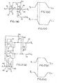
- FIG. 1(a) a conventional CMOS (Complementary-Metal-Oxide Semiconductor,) buffer circuit of the prior art and has been labeled "Prior Art".
- A represents an input
- a first stage gate 10 is composed of a P-channel transistor 12 and a N-channed transistor 14 which are coupled together to act as a CMOS inverter gate.
- Node 16 will maintain an inverted logic state with respect to the input logic signal A applied to line 18.
- a second stage gate 20 is composed of a P-channel transistor 22 and a N-channel transistor 24 which are coupled together to act as another CMOS inverter gate.
- the node 26 will maintain an inverted logic state with respect to the node 16.
- the node 26 is connected to the non-inverting output F at line 28, and the node 16 is connected to the inverting output F at line 30.
- Figures l(b) and l(c) illustrate the waveforms appearing at the outputs on the respective lines 28 and 30.
- the inverting output signal F on line 30 will be appearing before the non-inverting signal F on line 28 due to the inherent propagation delay in going through the second state gate 20.
- the outputs on lines 28 and 30 will not be symmetrical.
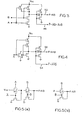
- the buffer circuit includes a CMOS inverter gate 32 formed of a P-channel transistor 34 and a N-channel transistor 36. Node 38 will maintain an inverter logic state with respect to node 40 to which the input logic signal A i is applied via input terminal 42.
- a first pair of N-channel MOS transistors Ql, Q2 have their drain electrodes coupled together.
- a second pair of N-channel MOS transistors Q3, Q4 have their drain electrodes coupled together.
- the input A i is applied via the input terminal 42 and node 40 to the gate electrodes of the transistors Q1 and Q4.
- the inverted input is applied via the node 38 to the gate electrodes of the transistors Q2 and Q3.
- a supply potential V OC is connected to the sources of the transistors Ql and Q3.
- the sources of the transistors Q2 and Q4 are connected to a ground potential.
- a pair of cross-coupled P-channel MOS transistors Q5, Q6 have their source electrodes tied together and to the supply potential V CC.
- the gate electrode of the transistor Q5 is connected to the drain of the transistor.
- Q6 and the gate of the transistor Q6 is connected to the drain of the transistor Q5.
- the drain of the transistor Q5 is also connected to the common drain of the transistors Ql, Q2 and to the non-inverting output F at line 44.
- the drain of the transistor Q6 is also connected to the common drain of the transistors Q3, Q4 and to the inverting output F at line 46. *
- Figures 2(b) and 2(c) illustrate the waveforms appearing at the outputs on the respective lines 44 and 46.
- the inverting output signal on line 46 will appear at the same time as the non-inverting output signal on line 44 without any propagation delay time.
- the outputs on the lines 44 and 46 will be symmetrical.
- FIG 5(a) there is shown a conventional * The inverter gate 32 is not required if the inverter input Ki is available from other previous circuits.
- the transmission gate design require true and complement input signals. However, it does not produce a complement output signal as in the conventional CMOS design.
- Figure 5(b) there is shown an alternate embodiment of a conventional transmission gate AND logic gate circuit which uses a reduced number of transistors than that of Figure 5(a). Nevertheless, it also does not produce a complement output signal.
- the AND logic gate circuit includes a first pair of N-channel type MOS transistors Q7, Q8; a second pair of N-channel type MOS transistors Q9, Q10; a third pair of N-channel type MOS transistors Qll, Q12; and a fourth pair of N-channel type MOS transistors Q13, Q14.
- the true input signal A is applied to the gate of the transistor Q7 of the first pair and to the gate of the transistor Q9 of the second pair.
- the complement input signal A is applied to the gate of the transistor Q8 of the first pair and to the gate of the transistor Q10 of the second pair.
- a supply potential V CC is connected to the sources of the transistors Q7 and Q10.
- the sources of the transistors Q8 and Q9 ae connected to a ground potential.
- the true input signal B is applied to the gate of the transistor Qll of the third pair and to the transistor Q13 of the fourth pair.
- the complement input signal B is applied to the gate of the transistor Q12 of the third pair and to the transistor Q14 of the fourth pair.
- the source of the transistor Q11 is connected to the drains of the transistors Q7, Q8 and the source of the transistor Q13 is connected to the drains of the transistors Q9, 010.
- the source of the transistor Q12 is connected to the ground potential, and the source of the transistor Q14 is connected to the supply potential Vcc-A pair of cross-coupled P-channel type MOS transistors Q15, Q16 have their sources connected to the supply potential V CC .
- the gate of the transistor Q15 is connected to the drain of the transistor Q16, and the gate of the transistor Q16 is connected to the drain of the transistor Q15.
- the drain of the transistor Q15 is also connected to the drains of the transistors Q11, Q12 of the third pair and to the true output F on line 64.
- the drain of the transistor Q16 is also connected to the drains of the transistors Q13, 014 of the fourth pair and to the complement output F on line 66.
- a buffered input signal is defined as one in which there is low impedance to ground in the low level state. Further, it should be apparent that a real "differential" will appear between the true output and complement output since one of the outputs will be near the supply potential V CC and the other output will be near the ground potential due to the pull-up action of the P-channel transistors Q15, Q16.
- a balanced CMOS multiplexer circuit of the present invention is illustrated in Figure 9.
- Inputs X 0 , X 1 , and X 2 represent true data signals and inputs X 0 , X 1 , and X 2 represent complement data signals.
- Inputs S 0 , S 1 , and S 2 represent control signals.
- Output F on line 68 represents the true output signal which is equal to the logical expression: S O X O + S 1 X 1 + S 2 X 2
- output F on line 70 represents the complement output signal which is equal to the logical expresssion: S 0 X 0 + S 1 X 1 + S 2 X 2 .
- the balanced multiplexer circuit includes a first pair of N-channel MOS transistors Q17, Q18; a second pair of N-channel MOS transistors Q19, Q20; a third pair of N-channel MOS transistors Q21, Q22; a fourth pair of N-channel MOS transistors Q23, Q24; a fifth pair of N-channel MOS transistors Q25, Q26; and a sixth pair of N-channel MOS transistors Q27, Q28.
- the true data signal X 0 is applied to the gate of the transistor Q17 of the first pair and to the gate of the transistor Q24 of the fourth pair.
- the complement data signal X 0 is applied to the gate of the transistor Q18 of the first pair and to the gate of the transistor Q23 of the fourth pair.
- the true data signal X 1 is applied to the gate of the transistor Q19 of the second pair and to the gate of transistor Q26 of the fifth pair.
- the complement data signal X 1 is applied to the gate of the transistor Q20 of the second pair and to the gate of the transistor Q25 of the fifth pair.
- the true data signal X 2 is applied to the gate of the transistor Q21 of the third pair and to the gate of the transistor Q28 of the sixth pair.
- the complement data signal X 2 is applied to the gate of the transistor Q 22 of the third pair and to the gate of the transistor Q27 of the sixth pair.
- a supply potential V CC is connected to the sources of the transistors Q17, Q19, Q21, Q23, Q25 and Q 27.
- the sources of the transistor Q18, Q20, Q22, Q24, Q26 and Q28 are connected to a ground potential.
- a first group of N-channel control transistors formed of MOS transistors Q29, Q30 and Q31 have their drains connected together.
- a second group of N-channel control transistors formed of MOS transistors Q32, Q33 and Q34 have their drains connected together.
- the drains of the transistors in each of the first through sixth pairs are connected together.
- the common drain of the first pair is also connected to the source of the transistor Q29.
- the common drains of the second through sixth pairs are also connected to the respective sources of the transistors Q30 through Q34.
- a pair of cross-coupled P-channel MOS transistors Q35 and Q36 have their sources connected to the supply potential V CC.
- the gate of the transistor Q35 is connected to the drain of the transistor Q36 and the gate of the transistor Q36 is connected to the drain of the transistor Q35.
- the drain of the transistor Q35 is further connected to the common drain of the first group of control transistors Q29, Q30 and Q31 and to the true output F on line 68.
- the drain of the transistor Q36 is connected to the common drain of the second group of control resistor Q32, Q33 and Q34 and to the complement output F on line 70.
- FIG. 10 An alternate embodiment of a balanced CMOS multiplexer circuit of the present invention is depicted in Figure 10 which requires a lesser number of N-channel transistors than that of Figure 9. As can be seen, this is due to the elimination of the N-channel transistors in the first through sixth pairs (017 through 028).
- the true data signals X 0 , X 1 , and X2 are applied directly to the respective sources of the transistors Q29, Q30 and Q31, and the complement data signals X 0 , X 1 and X2 are applied directly to the respective sources of the transistors Q32, Q33 and Q34.
- this circuit is identical to Figure 9. Again, this embodiment is possible only when the inputs are strong signals.
- the enclosed plus sign means "EXCLUSIVE-OR".
- the OR logic gate circuit includes a first pair of N-channel MOS transistors Q37, Q38; a second pair of N-channel MOS transistors Q39, 040; a third pair of N-channel MOS transistors Q41, Q42; and a fourth pair of N-channel os transistors Q43, Q44.
- the true input signal A is applied to the gate of the transistors Q37 and Q39.
- the complement input signal A is applied to the gates of the transistors Q38 and Q40.
- a supply potential V CC is applied to the sources of the transistors Q37 and Q40.
- the sources of the transistors Q38 and Q39 are tied to a ground potential.
- the true input signal B is applied to the gates of the transistors Q41 and Q43.
- the complement input signal B is applied to the gates of the transistors Q42 and Q44.
- the drains of the transistors Q37 and Q38 are tied together and further connected to the sources of the transistors Q41 and Q42.
- the drains of the transistors Q39 and Q40 are tied together and further connected to the sources of the transistors Q43 and Q44.
- a pair of cross-coupled P-channel MOS transistors Q45 and Q46 have their sources connected to the supply potential V CC .
- the gate of the transistor Q45 is connected to the drain of the transistor Q46 and the gate of the transistor Q46 is connected to the drain of the transistor Q45.
- the drain of the transistor Q 45 is also tied to the drains of the transistors Q41 and Q44 and to the complement output F on line 72.
- the drain of the transistor Q46 is also tied to the drains of the transistors Q42 and Q43 and to the true output F on line 74.
- FIG 12(a) there is shown a balanced CMOS D-type latch or flip-flop circuit.
- the D-type flip-flop circuit includes a first pair of N-channel MOS transistors Q47, Q48; a second pair of N-channel MOS transistors 049, 050; a third pair of N-channel MOS transistors Q51, Q52; and a fourth pair of N-channel MOS transistors Q53, Q54.
- the true input D is applied to the gates of the transistors Q47 and Q51.
- the complement input D is applied to the gates of the transistors Q48 and Q52.
- the true output Q on line 76 is applied as an input to the gates of the transistors Q49 and Q 53.
- the complement output Q on line 78 is applied as an input to the gates of the transistors Q50 and Q54.
- a supply potential V CC is connected to the sources of the transistors Q47, Q49, Q52 and Q54.
- the sources of the transistors Q48, Q50, Q51 and Q53 are tied to a ground potential.
- a first pair of N-channel clock transistors formed of MOS transistors Q55 and Q56 have their drains connected together.
- a second pair of N-channel clock transistors formed of MOS transistors Q57 and Q58 have their drains connected together.
- the true clock signal ⁇ is applied to the gates of the transistors Q55 and Q57.
- the complement clock signal ⁇ is applied to the gate of the transistor Q56 and Q58.
- the source of the transistor 055 is connected to the drains of the transistors Q47 and Q48.
- the source of the transistor Q56 is connected to the drains of the transistors Q49 and Q50.
- the source of the transistor Q57 is connected to the drains of the transistor Q51 and Q52.
- the source of the transistor Q58 is connected to the drains of the transistor Q53 and Q54.
- a pair of cross-coupled P-channel MOS transistors Q59 and Q60 have their drains connected to the supply potential 'è C .
- the gate of the transistor Q59 is connected to the drain of the transistor Q60 and the gate of the transistor Q60 is connected to the drain of the transistor Q59.
- the drain of the transistor Q59 is also connected to the common drain of the transistors Q55, Q56 and to the true output Q on the line 76.
- the drain of the transistor Q60 is also connected to the common drain of the transistors Q57, Q58 and to the complement output Q on the line 78.
- Figure 12(b) there is shown a representation of the circuit of Figure 12(a) in block diagram form.
- Two D-type flip-flop circuits of Figure 12(a) are shown in Figure 12(c) which is utilized to form a master-slave D-type flip-flop circuit.
- the present invention provides balanced CMOS logic gate circuits which are arranged on an integrated substrate with topological regularity so as to require a lesser amount of integrated surface area.
- the implementation of the various balanced CMOS logic gate circuits on such a substrate will minimize routing of interconnecting leads, thereby improving on the speed of operation.
Landscapes
- Engineering & Computer Science (AREA)
- Physics & Mathematics (AREA)
- Computer Hardware Design (AREA)
- Computing Systems (AREA)
- General Engineering & Computer Science (AREA)
- Mathematical Physics (AREA)
- Power Engineering (AREA)
- Logic Circuits (AREA)
Applications Claiming Priority (2)
| Application Number | Priority Date | Filing Date | Title |
|---|---|---|---|
| US688781 | 1985-01-04 | ||
| US06/688,781 US4620117A (en) | 1985-01-04 | 1985-01-04 | Balanced CMOS logic circuits |
Publications (2)
| Publication Number | Publication Date |
|---|---|
| EP0187697A2 true EP0187697A2 (fr) | 1986-07-16 |
| EP0187697A3 EP0187697A3 (fr) | 1988-10-26 |
Family
ID=24765739
Family Applications (1)
| Application Number | Title | Priority Date | Filing Date |
|---|---|---|---|
| EP86300025A Withdrawn EP0187697A3 (fr) | 1985-01-04 | 1986-01-03 | Circuit logiques CMOS équilibrés |
Country Status (3)
| Country | Link |
|---|---|
| US (1) | US4620117A (fr) |
| EP (1) | EP0187697A3 (fr) |
| JP (1) | JPS61199331A (fr) |
Cited By (3)
| Publication number | Priority date | Publication date | Assignee | Title |
|---|---|---|---|---|
| FR2618962A1 (fr) * | 1987-07-29 | 1989-02-03 | Intel Corp | Porte " ou exclusif " en technologie cmos |
| EP0511711A2 (fr) * | 1991-05-01 | 1992-11-04 | Koninklijke Philips Electronics N.V. | Circuit logique combinatoire programmable |
| GB2267614A (en) * | 1992-06-02 | 1993-12-08 | Plessey Semiconductors Ltd | Programmable logic cell |
Families Citing this family (33)
| Publication number | Priority date | Publication date | Assignee | Title |
|---|---|---|---|---|
| US4710649A (en) * | 1986-04-11 | 1987-12-01 | Raytheon Company | Transmission-gate structured logic circuits |
| US4910417A (en) * | 1986-09-19 | 1990-03-20 | Actel Corporation | Universal logic module comprising multiplexers |
| US5367208A (en) * | 1986-09-19 | 1994-11-22 | Actel Corporation | Reconfigurable programmable interconnect architecture |
| US4758744A (en) * | 1986-11-26 | 1988-07-19 | Rca Corporation | Decoder circuitry with reduced number of inverters and bus lines |
| FR2609585B1 (fr) * | 1987-01-13 | 1991-03-15 | Labo Electronique Physique | Circuit realisant la fonction ou-exclusif |
| JPH02222217A (ja) * | 1989-02-22 | 1990-09-05 | Toshiba Corp | プログラマブル論理回路 |
| US5475631A (en) * | 1989-03-09 | 1995-12-12 | Micron Technology, Inc. | Multiport RAM based multiprocessor |
| US4912665A (en) * | 1989-03-13 | 1990-03-27 | Micron Technology, Inc. | Arithmetic logic unit capable of having a narrow pitch |
| US4970677A (en) * | 1989-06-05 | 1990-11-13 | Harris Corporation | Full adder circuit with improved carry and sum logic gates |
| US5155387A (en) * | 1989-12-28 | 1992-10-13 | North American Philips Corp. | Circuit suitable for differential multiplexers and logic gates utilizing bipolar and field-effect transistors |
| KR950004745B1 (ko) * | 1990-01-23 | 1995-05-06 | 니뽄 덴끼 가부시끼가이샤 | 반도체 디지탈 회로 |
| US5039883A (en) * | 1990-02-21 | 1991-08-13 | Nec Electronics Inc. | Dual input universal logic structure |
| US5015881A (en) * | 1990-03-02 | 1991-05-14 | International Business Machines Corp. | High speed decoding circuit with improved AND gate |
| US5198705A (en) * | 1990-05-11 | 1993-03-30 | Actel Corporation | Logic module with configurable combinational and sequential blocks |
| US5055718A (en) * | 1990-05-11 | 1991-10-08 | Actel Corporation | Logic module with configurable combinational and sequential blocks |
| US5416367A (en) * | 1991-03-06 | 1995-05-16 | Quicklogic Corporation | Programmable application specific integrated circuit and logic cell therefor |
| US5122685A (en) * | 1991-03-06 | 1992-06-16 | Quicklogic Corporation | Programmable application specific integrated circuit and logic cell therefor |
| US5126596A (en) * | 1991-03-18 | 1992-06-30 | Motorola, Inc. | Transmission gate having a pass transistor with feedback |
| US5528177A (en) * | 1994-09-16 | 1996-06-18 | Research Foundation Of State University Of New York | Complementary field-effect transistor logic circuits for wave pipelining |
| US5508641A (en) * | 1994-12-20 | 1996-04-16 | International Business Machines Corporation | Integrated circuit chip and pass gate logic family therefor |
| US5568069A (en) * | 1995-02-27 | 1996-10-22 | Hughes Aircraft Company | High speed, low power pipelined logic circuit |
| US5777491A (en) * | 1995-03-31 | 1998-07-07 | International Business Machines Corporation | High-performance differential cascode voltage switch with pass gate logic elements |
| JPH0993118A (ja) * | 1995-09-22 | 1997-04-04 | Kawasaki Steel Corp | パストランジスタ論理回路 |
| US6097221A (en) * | 1995-12-11 | 2000-08-01 | Kawasaki Steel Corporation | Semiconductor integrated circuit capable of realizing logic functions |
| US5598114A (en) * | 1995-09-27 | 1997-01-28 | Intel Corporation | High speed reduced area multiplexer |
| US5719507A (en) * | 1995-10-12 | 1998-02-17 | Xilinx, Inc. | Logic gate having transmission gate for electrically configurable device multiplexer |
| US5936426A (en) * | 1997-02-03 | 1999-08-10 | Actel Corporation | Logic function module for field programmable array |
| US6040717A (en) * | 1997-07-28 | 2000-03-21 | I.C. Com Ltd. | FRCPG: Forecasted restoration complementary pass gates |
| US6069495A (en) * | 1997-11-21 | 2000-05-30 | Vsli Technology, Inc. | High-speed logic embodied differential dynamic CMOS true single phase clock latches and flip-flops with single transistor clock latches |
| US6288593B1 (en) | 2000-01-04 | 2001-09-11 | Translogic Technology, Inc. | Digital electronic circuit for use in implementing digital logic functions |
| US6252426B1 (en) * | 2000-03-07 | 2001-06-26 | Honeywell International Inc. | High speed logic family |
| US6501817B2 (en) | 2000-08-25 | 2002-12-31 | United Memories, Inc. | Area efficient redundancy multiplexer circuit technique for integrated circuit devices providing significantly reduced parasitic capacitance |
| US7336104B2 (en) * | 2004-06-28 | 2008-02-26 | Technion Research & Development Foundation Ltd. | Multiple-output transistor logic circuit |
Citations (2)
| Publication number | Priority date | Publication date | Assignee | Title |
|---|---|---|---|---|
| EP0094234A2 (fr) * | 1982-05-10 | 1983-11-16 | American Microsystems, Incorporated | Structure logique combinatoire utilisant des transistors de couplage |
| EP0130363A2 (fr) * | 1983-06-27 | 1985-01-09 | International Business Machines Corporation | Circuit logique différentiel réalisé en technologie à transistors complémentaires |
Family Cites Families (2)
| Publication number | Priority date | Publication date | Assignee | Title |
|---|---|---|---|---|
| JPS5597734A (en) * | 1979-01-19 | 1980-07-25 | Toshiba Corp | Logic circuit |
| US4367420A (en) * | 1980-06-02 | 1983-01-04 | Thompson Foss Incorporated | Dynamic logic circuits operating in a differential mode for array processing |
-
1985
- 1985-01-04 US US06/688,781 patent/US4620117A/en not_active Expired - Lifetime
- 1985-12-28 JP JP60299817A patent/JPS61199331A/ja active Pending
-
1986
- 1986-01-03 EP EP86300025A patent/EP0187697A3/fr not_active Withdrawn
Patent Citations (2)
| Publication number | Priority date | Publication date | Assignee | Title |
|---|---|---|---|---|
| EP0094234A2 (fr) * | 1982-05-10 | 1983-11-16 | American Microsystems, Incorporated | Structure logique combinatoire utilisant des transistors de couplage |
| EP0130363A2 (fr) * | 1983-06-27 | 1985-01-09 | International Business Machines Corporation | Circuit logique différentiel réalisé en technologie à transistors complémentaires |
Non-Patent Citations (2)
| Title |
|---|
| IBM TECHNICAL DISCLOSURE BULLETIN, vol. 27, no. 1B, June 1984, page 654, New York, US; J.A. HILTEBEITEL: "And-or-and-or-invert (AOAOI) cascode voltage switch" * |
| IBM TECHNICAL DISCLOSURE BULLETIN, vol. 27, no. 1B, June 1984, pages 657-658, New York, US; W.J. CRAIG et al.: "CVS logic circuit with decoupled outputs" * |
Cited By (6)
| Publication number | Priority date | Publication date | Assignee | Title |
|---|---|---|---|---|
| FR2618962A1 (fr) * | 1987-07-29 | 1989-02-03 | Intel Corp | Porte " ou exclusif " en technologie cmos |
| EP0511711A2 (fr) * | 1991-05-01 | 1992-11-04 | Koninklijke Philips Electronics N.V. | Circuit logique combinatoire programmable |
| EP0511711A3 (en) * | 1991-05-01 | 1995-03-15 | Philips Nv | Programmable combinational logic circuit |
| GB2267614A (en) * | 1992-06-02 | 1993-12-08 | Plessey Semiconductors Ltd | Programmable logic cell |
| US5418480A (en) * | 1992-06-02 | 1995-05-23 | Plessey Semiconductors Limited | Logic cell using only two N type transistors for generating each logic function |
| GB2267614B (en) * | 1992-06-02 | 1996-01-24 | Plessey Semiconductors Ltd | Logic cell |
Also Published As
| Publication number | Publication date |
|---|---|
| JPS61199331A (ja) | 1986-09-03 |
| US4620117A (en) | 1986-10-28 |
| EP0187697A3 (fr) | 1988-10-26 |
Similar Documents
| Publication | Publication Date | Title |
|---|---|---|
| EP0187697A2 (fr) | Circuit logiques CMOS équilibrés | |
| US4568842A (en) | D-Latch circuit using CMOS transistors | |
| US4920284A (en) | CMOS level converter circuit with reduced power consumption | |
| US4558236A (en) | Universal logic circuit | |
| US4506165A (en) | Noise rejection Set-Reset Flip-Flop circuitry | |
| US4150308A (en) | CMOS level shifter | |
| US5045730A (en) | Electrical circuitry providing compatibility between different logic levels | |
| US5170074A (en) | Master-slave clocked flip-flop circuit | |
| US4689763A (en) | CMOS full adder circuit | |
| KR100686983B1 (ko) | 레벨 컨버터 회로 | |
| US4591742A (en) | Output circuit capable of being connected to another circuit having transistors of any conduction type | |
| US4962471A (en) | High speed digital carry look ahead circuit for parallel adder | |
| US6967505B2 (en) | Input circuit | |
| KR100379607B1 (ko) | 래치 회로 | |
| US4631425A (en) | Logic gate circuit having P- and N- channel transistors coupled in parallel | |
| US4739503A (en) | Carry/borrow propagate adder/subtractor | |
| KR890005996A (ko) | 동기 플립플롭회로 | |
| US5994936A (en) | RS flip-flop with enable inputs | |
| JPH0614609B2 (ja) | 論理ゲ−ト・アレイ | |
| EP1130780B1 (fr) | Circuit logique intégré semi-conducteur | |
| US4259595A (en) | Clocking system for MOS transistor logic circuit | |
| JPS6037822A (ja) | Cmos論理回路 | |
| KR100202179B1 (ko) | 4비트 이븐 패리티 비트 발생 회로 | |
| JPH0446014B2 (fr) | ||
| KR970006626B1 (ko) | 고속 d- 플립플롭 회로 |
Legal Events
| Date | Code | Title | Description |
|---|---|---|---|
| PUAI | Public reference made under article 153(3) epc to a published international application that has entered the european phase |
Free format text: ORIGINAL CODE: 0009012 |
|
| AK | Designated contracting states |
Kind code of ref document: A2 Designated state(s): AT BE CH DE FR GB IT LI LU NL SE |
|
| PUAL | Search report despatched |
Free format text: ORIGINAL CODE: 0009013 |
|
| AK | Designated contracting states |
Kind code of ref document: A3 Designated state(s): AT BE CH DE FR GB IT LI LU NL SE |
|
| 17P | Request for examination filed |
Effective date: 19890413 |
|
| ITF | It: translation for a ep patent filed | ||
| 17Q | First examination report despatched |
Effective date: 19900814 |
|
| STAA | Information on the status of an ep patent application or granted ep patent |
Free format text: STATUS: THE APPLICATION IS DEEMED TO BE WITHDRAWN |
|
| 18D | Application deemed to be withdrawn |
Effective date: 19910226 |
|
| RIN1 | Information on inventor provided before grant (corrected) |
Inventor name: FANG, SHENG |