EP0186595B1 - Technique d'acheminement - Google Patents
Technique d'acheminement Download PDFInfo
- Publication number
- EP0186595B1 EP0186595B1 EP85402585A EP85402585A EP0186595B1 EP 0186595 B1 EP0186595 B1 EP 0186595B1 EP 85402585 A EP85402585 A EP 85402585A EP 85402585 A EP85402585 A EP 85402585A EP 0186595 B1 EP0186595 B1 EP 0186595B1
- Authority
- EP
- European Patent Office
- Prior art keywords
- signal
- address
- input
- output
- signals
- Prior art date
- Legal status (The legal status is an assumption and is not a legal conclusion. Google has not performed a legal analysis and makes no representation as to the accuracy of the status listed.)
- Expired
Links
Images


Classifications
-
- H—ELECTRICITY
- H04—ELECTRIC COMMUNICATION TECHNIQUE
- H04L—TRANSMISSION OF DIGITAL INFORMATION, e.g. TELEGRAPHIC COMMUNICATION
- H04L49/00—Packet switching elements
- H04L49/25—Routing or path finding in a switch fabric
-
- G—PHYSICS
- G06—COMPUTING; CALCULATING OR COUNTING
- G06F—ELECTRIC DIGITAL DATA PROCESSING
- G06F7/00—Methods or arrangements for processing data by operating upon the order or content of the data handled
- G06F7/22—Arrangements for sorting or merging computer data on continuous record carriers, e.g. tape, drum, disc
- G06F7/24—Sorting, i.e. extracting data from one or more carriers, rearranging the data in numerical or other ordered sequence, and rerecording the sorted data on the original carrier or on a different carrier or set of carriers sorting methods in general
-
- H—ELECTRICITY
- H04—ELECTRIC COMMUNICATION TECHNIQUE
- H04Q—SELECTING
- H04Q3/00—Selecting arrangements
- H04Q3/64—Distributing or queueing
- H04Q3/68—Grouping or interlacing selector groups or stages
-
- G—PHYSICS
- G06—COMPUTING; CALCULATING OR COUNTING
- G06F—ELECTRIC DIGITAL DATA PROCESSING
- G06F2207/00—Indexing scheme relating to methods or arrangements for processing data by operating upon the order or content of the data handled
- G06F2207/22—Indexing scheme relating to groups G06F7/22 - G06F7/36
- G06F2207/228—Sorting or merging network
-
- H—ELECTRICITY
- H04—ELECTRIC COMMUNICATION TECHNIQUE
- H04L—TRANSMISSION OF DIGITAL INFORMATION, e.g. TELEGRAPHIC COMMUNICATION
- H04L49/00—Packet switching elements
- H04L49/15—Interconnection of switching modules
-
- H—ELECTRICITY
- H04—ELECTRIC COMMUNICATION TECHNIQUE
- H04L—TRANSMISSION OF DIGITAL INFORMATION, e.g. TELEGRAPHIC COMMUNICATION
- H04L49/00—Packet switching elements
- H04L49/15—Interconnection of switching modules
- H04L49/1515—Non-blocking multistage, e.g. Clos
- H04L49/1546—Non-blocking multistage, e.g. Clos using pipelined operation
-
- H—ELECTRICITY
- H04—ELECTRIC COMMUNICATION TECHNIQUE
- H04L—TRANSMISSION OF DIGITAL INFORMATION, e.g. TELEGRAPHIC COMMUNICATION
- H04L49/00—Packet switching elements
- H04L49/40—Constructional details, e.g. power supply, mechanical construction or backplane
Definitions
- the invention relates to circuits for routing signals to specific lines, based on the address of each signal.
- Circuit elements are arrayed so as to throughput a signal from any of a number of inputs to a specific output based on a signal characteristic, such as an address header on a digital byte.
- Each element has two inputs, a "low” and a “high” output, and an internal address.
- the characteristic of two input signals are compared in the circuit element; the signal having the greater characteristic is throughput in the "high” output and the signal having the lesser characteristic is throughput to the "low” output.
- the element's internal address and throughput to the "low” output if it is less than or equal thereto. Otherwise it is throughput to the "high” output.
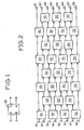
- Fig. 1 discloses a prior art bubble sort element 10 that compares the magnitude of signals impressed upon two inputs (A) and (B), and throughputs the signal of lesser magnitude to a "low” output (L) and the signal of the greater magnitude to a "high” output (H).
- the addresses of address-bearing data are compared by the element 10. The data bearing the lesser address is throughput to the "low” output (L), and the data bearing the greater address is throughput to the "high” output (H).
- the other input is null (N), and the input signal will be throughputto the "high” output (H) since it is ipso facto of greater magnitude.
- elements 10 are arrayed in a "brick-wall" structure so that signals presented to the inputs 11-18 are sorted according to magnitude at the outputs 21-28.
- the input signal having the greatest magnitude is sorted to the "highest" output 28, the signal having the next lower magnitude to the output 27, the signal having the next tower magnitude to the output 26, and so forth, filling the outputs 21-28 with sorted signals.
- Other interconnection techniques for achieving the same function are disclosed in U.S. Patents No. 3,428,946 (Batcher, 1969), entitled MEANS FOR MERGING DATA; No.
- null inputs (N) In the case of null inputs (N)-in other words, fewer than all of the inputs having signals impressed thereon-the signals are sorted to the higher numbered outputs since the null inputs will "rise” to the lower numbered inputs. Thus, the output to which an input signal is sorted is dependent upon the contingency of null inputs (N). Because of this dependency, these sort techniques are not suited to "routing". For routing, the criteria is that input data be uniquely routed to a specific output, regardless of the input upon which it is impressed and whether there are null inputs (N). Nevertheless, sorting techniques provide a useful backdrop against which to highlight the invention.
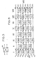
- Fig. 3 is shown a modified bubble sort element 30 that has an address (n) associated therewith.
- address-bearing data bytes
- the addresses of the bytes are compared, and the byte having the lesser address is throughput to a "low" output (L) and the byte having the greater address is throughput to a "high” output (H).
- the other input is considered null (N) and the comparison is made between the address of the byte and the element address (n).
- the byte is throughput to the "low” output (L) if its address is less than or equal to (n), or to the "high” output (H) if its address is greater than (n).
- the null input (N) is throughput to the other output. In the case of two null inputs (N), the outputs (L, H) are null.
- Fig. 4 discloses a circuit for the element 30.
- a similarly-sized byte (R) is presented to the input (B).
- a buffer 32 isolates the address of the byte (Q) and presents it on a line 33 to a value comparator 34 where it is compared to ZERO to test for a null input (N) on the input (A), in which case a logic ONE is provided on a line 35 to a multiplex switch 36.
- a buffer 38 isolates the address of the byte (R) and presents it on a line 39 to a value comparator 40 where it is compared to ZERO to test for a null input (N) on the input (B), in which case a logic ONE is provided on a line 41 to a multiplex switch 42. It would be equivalent to locate the buffers 32, 38 in the lines 33, 39 respectively, so that the entire bytes were compared ZERO for non input detection.
- An address means such as a constant generator 44 provides an address (n) on a line 45 to one input of each multiplexer 36, 42.
- the address means may also be hard wired, a dip- switch, or a ROM.
- the multiplexer 36 In response to the output of the comparator 34, the multiplexer 36 throughputs the address of the byte (Q) or, in the case of a null input (N) on the input (A), throughputs the stored address (n) to a line 46. Similarly, in response to the output of the comparator 40 the multiplexer 42 throughputs the address of the byte (R) or, in the case of a null input (N) on the input (B), throughputs the stored address (n) to a line 48.
- a comparator 50 is responsive to the throughputs of the multiplexers 36, 42 and provides a logic ONE on a line 51 to an OR gate 52 if the address on the line 46 is greater than the address on the line 48.
- the output of the OR gate 52 on a line 53 controls two multiplex switches 54 and 56, the latter via an inverter 58. These switches 54, 56 are operable to throughput the signals on the inputs (A) and (B) to the outputs (L) and (H) based on the output of the comparator 50. Therefore, if the address of the byte (Q) is less than the address of the byte (R); (A) is less than (B), the output of the comparator 50 is ZERO, the switch 56 throughputs the byte (Q) to the (L) output, and the switch 58 throughputs the byte (R) to the (H) output.
- a comparator 58 is also responsive to throughputs of the multiplexers 36, 42 and provides a logic ONE on a line 59 to an AND gate 60 if the address on the line 46 equals the address on the line 48. This can happen if both bytes (Q) and (R) have the same address, if both inputs (A) and (B) are null (N), or if one input is null and the address of the byte on the other input equals (n). If the input (A) is also null (n), a logic ONE is provided by the comparator 34 on the line 35 to the AND gate 60 so that a logic ONE is provided on a line 61 to the OR gate 52.
- Fig. 5 shows a technique for interconnecting and addressing several elements 30 so that signals presented to the 71-78 are uniquely routed to outputs 81-88 according to the value of a characteristic, such as their address. It will be noted that the interconnection of the elements 30 is identical to the interconnection of elements 10 in the generalized sorting technique discussed with reference to Fig. 2. The routing technique is discussed for eight inputs and eight outputs, but is applicable to routing more or fewer data.
- the elements 30 are labeled 30a-30bb and their internal addresses (n) are in parentheses.
- the outputs 81-88 are ordered, and correspond to address values 1-8, respectively.
- the object is that data bearing the address SEVEN, for instance, is routed to the output 87, regardless of which input 71-78 it is impressed upon and whether there are signals on the other inputs.
- the "brick wall” array of elements 30 involves eight routing stages (I-VIII).
- the four elements 30a-30d each receive a pair of the eight inputs 71-78 on their A/B inputs and route signals impressed thereon to their eight L/ H outputs, which are signal lines 81'-88' that correspond in value to the outputs 81-88.
- an element 30 can route a signal one line 81'-88' nearer to its ultimate destination 81-88.
- the elements 30c-30g of stage II receive the lines 82'-87' in an ordered hierarchial manner for comparison of adjacent lines. There are three, rather than four elements at this stage, since it would be redundant to make the same four comparisions as in stage I. Comparisons are made between the H output of element 30a and the L output of the element 30b, between the H output of the element 30b and the L output of the element 30c, and between the H output of the element 30c and the L output of the element 30d.
- stage III the ordered outputs of stage III are compared in four comparisions of adjacent pairs of the lines 81'-88'.
- Stages IV, VI and VIII are akin to stage II and stages V and VII are akin to stages I and III so that the eight stages I-VIII accomplish the routing technique of this invention.
- a byte (S), bearing the address FOUR, is presented at the input 76 to the input (B) of the element 30c. All other inputs 71-75, 77-78 are null inputs (N). Since the address associated with the element 30c is FIVE, the byte (S) is routed to the "low" output (L), which is connected to the input (B) of the element 30f by the line 85'. The address of the element 30f is FOUR, so the byte (S) is routed to the "low” output (L) on the line 84', which is connected to the input (B) of the element 30i.
- the address of the element 30i is THREE, so the byte (S) is routed to the "high” output (H) on the line 84', which is connected to the input (A) of the element 30m.
- the address of the element 30m is FOUR, so the byte (S) is routed to the "low” output (L) on the line 84', which is connected to the input (B) of the element 30p and so on, as shown, until the byte (S) arrives at the output 84.
- the routing technique is ideally suited to an even number (2X) of inputs/outputs, but could be adapted to an odd number.
- the routing technique employs a high-bandwidth solution with 0(n) latency and does not limit the number of input wires or restrict the number of conversations that can be made at any time (e.g. it is non-blocking).
- Control of the routing technique is reduced to inputting the correct destination address with each input datum.
- This problem could get complex except that the input of address is cyclic with the number of conversations multiplexed on a line.
- Figure 6 shows a shift register controller which could be used to contain the address information for the data input line. The shift register need only be changed when a conversation is started or finished.
- This design does not solve the problem of time- switching. That is, if two time-multiplexed signals attempt to go to the same output wire at the same input time-slot (regardless of the desired output- time slot) this system will fail. However, the physical analog crossbar will also fail in the same way and it is known to place time-multiplexing units at either end of the crossbar to prevent time-data collision. The memory storage solution of this problem does not have this time-data collision problem since its implementation also time- sorts.
- the routing technique is applicable to the routing of any high-bandwidth input data. It would be especially good as a terminal-to-computer data switch.
- the modular design of the routing technique lends itself to VLSI or perhaps wafer scale implementation, since the node design could be made fault tolerant and since redundant nodes can easily be added to the network.
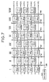
- the routing technique described with reference to Fig. 5 is especially well suited to a pipelined configuration, such as is shown in Fig. 7.
- storage registers 90-96 are placed at the output of each stage (I-Vil).
- the output of each stage is stored in the respective register until a signal on a line 98 from a controller 100 causes the registers 90-96 to throughput the signals to the next stage of the routing process.
- the throughput (bandwidth) of the system can be tailored thereby to a specific input rate, such as the standard 130ns per bit input rate of phone lines. This method puts no constraints on the number of incoming phone lines and the only time penalty paid is O(n) latency on output, which is unimportant in this particular application.
Landscapes
- Engineering & Computer Science (AREA)
- Computer Networks & Wireless Communication (AREA)
- General Engineering & Computer Science (AREA)
- Theoretical Computer Science (AREA)
- Signal Processing (AREA)
- Computer Hardware Design (AREA)
- Physics & Mathematics (AREA)
- General Physics & Mathematics (AREA)
- Data Exchanges In Wide-Area Networks (AREA)
Claims (4)
Applications Claiming Priority (2)
| Application Number | Priority Date | Filing Date | Title |
|---|---|---|---|
| US686314 | 1984-12-24 | ||
| US06/686,314 US4685128A (en) | 1984-12-24 | 1984-12-24 | Method and network for transmitting addressed signal samples from any network input to an addressed network output |
Publications (3)
| Publication Number | Publication Date |
|---|---|
| EP0186595A2 EP0186595A2 (fr) | 1986-07-02 |
| EP0186595A3 EP0186595A3 (en) | 1988-04-20 |
| EP0186595B1 true EP0186595B1 (fr) | 1989-08-23 |
Family
ID=24755814
Family Applications (1)
| Application Number | Title | Priority Date | Filing Date |
|---|---|---|---|
| EP85402585A Expired EP0186595B1 (fr) | 1984-12-24 | 1985-12-20 | Technique d'acheminement |
Country Status (3)
| Country | Link |
|---|---|
| US (1) | US4685128A (fr) |
| EP (1) | EP0186595B1 (fr) |
| DE (1) | DE3572578D1 (fr) |
Families Citing this family (5)
| Publication number | Priority date | Publication date | Assignee | Title |
|---|---|---|---|---|
| US4758981A (en) * | 1984-12-24 | 1988-07-19 | Sgs-Thomson Microelectronics, Inc. | Signal sorting element with internal signal address value sorting criterion |
| US4817084A (en) * | 1986-10-16 | 1989-03-28 | Bell Communications Research, Inc. | Batcher-Banyan packet switch with output conflict resolution scheme |
| EP0309670B1 (fr) * | 1987-09-29 | 1994-04-13 | Siemens Aktiengesellschaft | Concentrateur pour une réseau rapide de commutation de données |
| US6271693B1 (en) * | 1997-12-12 | 2001-08-07 | United Microelectronics Corp. | Multi-function switched-current magnitude sorter |
| GB2365660A (en) * | 2000-03-10 | 2002-02-20 | British Telecomm | Circuit switching |
Family Cites Families (13)
| Publication number | Priority date | Publication date | Assignee | Title |
|---|---|---|---|---|
| US3435417A (en) * | 1965-08-04 | 1969-03-25 | Sylvania Electric Prod | Electronic switching system |
| US3428946A (en) * | 1965-08-26 | 1969-02-18 | Goodyear Aerospace Corp | Means for merging data |
| US3593295A (en) * | 1968-05-10 | 1971-07-13 | Bell Telephone Labor Inc | Rearrangeable switching network |
| US3638193A (en) * | 1970-02-02 | 1972-01-25 | Bell Telephone Labor Inc | {62 -element switching network control |
| AT318018B (de) * | 1970-07-21 | 1974-09-25 | Siemens Ag | Koppelanordnung mit einer Mehrzahl von untereinander verbundenen, jeweils nur zwei erste und zwei zweite Leitungen aufweisenden Koppelvielfachen (Binärkopplern) |
| US3694580A (en) * | 1971-07-28 | 1972-09-26 | Bell Telephone Labor Inc | Time division switching system |
| US3963872A (en) * | 1974-06-03 | 1976-06-15 | North Electric Company | Non-symmetric folded four-stage switching network |
| US3976845A (en) * | 1975-12-08 | 1976-08-24 | Gte Sylvania Incorporated | Switching network having improved turn-on capability |
| US4075608A (en) * | 1976-01-19 | 1978-02-21 | The United States Of America As Represented By The Secretary Of The Navy | Multiple-channel data switch |
| US4186277A (en) * | 1976-01-23 | 1980-01-29 | Siemens Aktiengesellschaft | Time division multiplex telecommunications switching network |
| US4307466A (en) * | 1980-01-15 | 1981-12-22 | Goldschmidt Hugh A C | Audio system for drive-in theaters |
| JPS56110149A (en) * | 1980-02-05 | 1981-09-01 | Nec Corp | Parallel classification processing device |
| US4758981A (en) * | 1984-12-24 | 1988-07-19 | Sgs-Thomson Microelectronics, Inc. | Signal sorting element with internal signal address value sorting criterion |
-
1984
- 1984-12-24 US US06/686,314 patent/US4685128A/en not_active Expired - Lifetime
-
1985
- 1985-12-20 DE DE8585402585T patent/DE3572578D1/de not_active Expired
- 1985-12-20 EP EP85402585A patent/EP0186595B1/fr not_active Expired
Also Published As
| Publication number | Publication date |
|---|---|
| DE3572578D1 (en) | 1989-09-28 |
| EP0186595A3 (en) | 1988-04-20 |
| US4685128A (en) | 1987-08-04 |
| EP0186595A2 (fr) | 1986-07-02 |
Similar Documents
| Publication | Publication Date | Title |
|---|---|---|
| US4516238A (en) | Self-routing switching network | |
| US4918686A (en) | Data transfer network suitable for use in a parallel computer | |
| KR19980084431A (ko) | 고속 패킷 스위칭을 위한 다단 상호 연결 망 | |
| US5016245A (en) | Modular expandable digital single-stage switching network in ATM (Asynchronous Transfer Mode) technology for a fast packet-switched transmission of information | |
| US5612952A (en) | Packet switch and buffer for storing and processing packets routing to different ports | |
| Koppelman et al. | A self-routing permutation network | |
| WO1991005375A1 (fr) | Procede et appareil permettant de simuler un reseau d'interconnexion | |
| US5319639A (en) | Crossbar with return net for scalable self-routing non-blocking message switching and routing system | |
| US4910730A (en) | Batcher-banyan network | |
| JPH03218144A (ja) | 高速パケット交換機 | |
| EP0186595B1 (fr) | Technique d'acheminement | |
| US5216420A (en) | Matrix sorting network for sorting N inputs onto N outputs | |
| US5043980A (en) | Switching cell for packet switching network | |
| US5220664A (en) | Merging network with three or more simultaneous inputs | |
| US5175539A (en) | Interconnecting network | |
| CA2006392C (fr) | Reseau de commutation mono-menage numerique modulaire extensible fonctionnant en mode de transfert asynchrone pour la transmission rapide d'informations par commutation de paquets | |
| JP2954220B2 (ja) | 並列計算機のためのデータ転送ネットワーク | |
| JP2008160522A (ja) | 多段スイッチの制御回路 | |
| JPH10294746A (ja) | Nビットセットのうちのmビットセットを置換するためのインターフェース装置、制御ユニット、および論理セル | |
| JPH0865318A (ja) | 非同期転送モード・データ・セル・ルーティング装置 | |
| Lee et al. | New self-routing permutation networks | |
| Jajszczyk et al. | Optimization of large-scale growable ATM switching fabrics | |
| JP3002659B2 (ja) | データ転送ネットワーク | |
| JP2803209B2 (ja) | パケットスイッチ | |
| JP4158264B2 (ja) | ソート・マージ処理装置およびソート・マージ回路 |
Legal Events
| Date | Code | Title | Description |
|---|---|---|---|
| PUAI | Public reference made under article 153(3) epc to a published international application that has entered the european phase |
Free format text: ORIGINAL CODE: 0009012 |
|
| AK | Designated contracting states |
Kind code of ref document: A2 Designated state(s): DE FR GB IT NL |
|
| PUAL | Search report despatched |
Free format text: ORIGINAL CODE: 0009013 |
|
| AK | Designated contracting states |
Kind code of ref document: A3 Designated state(s): DE FR GB IT NL |
|
| 17P | Request for examination filed |
Effective date: 19880721 |
|
| 17Q | First examination report despatched |
Effective date: 19881110 |
|
| RAP1 | Party data changed (applicant data changed or rights of an application transferred) |
Owner name: SGS-THOMSON MICROELECTRONICS, INC. (A DELAWARE COR |
|
| GRAA | (expected) grant |
Free format text: ORIGINAL CODE: 0009210 |
|
| AK | Designated contracting states |
Kind code of ref document: B1 Designated state(s): DE FR GB IT NL |
|
| REF | Corresponds to: |
Ref document number: 3572578 Country of ref document: DE Date of ref document: 19890928 |
|
| ITF | It: translation for a ep patent filed |
Owner name: JACOBACCI & PERANI S.P.A. |
|
| ET | Fr: translation filed | ||
| PGFP | Annual fee paid to national office [announced via postgrant information from national office to epo] |
Ref country code: NL Payment date: 19891231 Year of fee payment: 5 |
|
| PLBE | No opposition filed within time limit |
Free format text: ORIGINAL CODE: 0009261 |
|
| STAA | Information on the status of an ep patent application or granted ep patent |
Free format text: STATUS: NO OPPOSITION FILED WITHIN TIME LIMIT |
|
| 26N | No opposition filed | ||
| ITTA | It: last paid annual fee | ||
| PG25 | Lapsed in a contracting state [announced via postgrant information from national office to epo] |
Ref country code: NL Effective date: 19910701 |
|
| NLV4 | Nl: lapsed or anulled due to non-payment of the annual fee | ||
| PGFP | Annual fee paid to national office [announced via postgrant information from national office to epo] |
Ref country code: DE Payment date: 19971230 Year of fee payment: 13 |
|
| PG25 | Lapsed in a contracting state [announced via postgrant information from national office to epo] |
Ref country code: DE Free format text: LAPSE BECAUSE OF NON-PAYMENT OF DUE FEES Effective date: 19991001 |
|
| PGFP | Annual fee paid to national office [announced via postgrant information from national office to epo] |
Ref country code: FR Payment date: 20011212 Year of fee payment: 17 |
|
| PGFP | Annual fee paid to national office [announced via postgrant information from national office to epo] |
Ref country code: GB Payment date: 20011219 Year of fee payment: 17 |
|
| REG | Reference to a national code |
Ref country code: GB Ref legal event code: IF02 |
|
| PG25 | Lapsed in a contracting state [announced via postgrant information from national office to epo] |
Ref country code: GB Free format text: LAPSE BECAUSE OF NON-PAYMENT OF DUE FEES Effective date: 20021220 |
|
| GBPC | Gb: european patent ceased through non-payment of renewal fee |
Effective date: 20021220 |
|
| PG25 | Lapsed in a contracting state [announced via postgrant information from national office to epo] |
Ref country code: FR Free format text: LAPSE BECAUSE OF NON-PAYMENT OF DUE FEES Effective date: 20030901 |
|
| REG | Reference to a national code |
Ref country code: FR Ref legal event code: ST |