EP0186443B1 - Silicon nitride films for integrated circuits - Google Patents
Silicon nitride films for integrated circuits Download PDFInfo
- Publication number
- EP0186443B1 EP0186443B1 EP85309262A EP85309262A EP0186443B1 EP 0186443 B1 EP0186443 B1 EP 0186443B1 EP 85309262 A EP85309262 A EP 85309262A EP 85309262 A EP85309262 A EP 85309262A EP 0186443 B1 EP0186443 B1 EP 0186443B1
- Authority
- EP
- European Patent Office
- Prior art keywords
- silicon nitride
- silane
- approximately
- ammonia
- chamber
- Prior art date
- Legal status (The legal status is an assumption and is not a legal conclusion. Google has not performed a legal analysis and makes no representation as to the accuracy of the status listed.)
- Expired - Lifetime
Links
- 229910052581 Si3N4 Inorganic materials 0.000 title claims abstract description 50
- HQVNEWCFYHHQES-UHFFFAOYSA-N silicon nitride Chemical compound N12[Si]34N5[Si]62N3[Si]51N64 HQVNEWCFYHHQES-UHFFFAOYSA-N 0.000 title claims abstract description 48
- 229910021529 ammonia Inorganic materials 0.000 claims abstract description 26
- 238000002161 passivation Methods 0.000 claims abstract description 20
- 238000006243 chemical reaction Methods 0.000 claims abstract description 18
- 230000005855 radiation Effects 0.000 claims abstract description 10
- QGZKDVFQNNGYKY-UHFFFAOYSA-N Ammonia Chemical compound N QGZKDVFQNNGYKY-UHFFFAOYSA-N 0.000 claims description 33
- 238000000034 method Methods 0.000 claims description 26
- BLRPTPMANUNPDV-UHFFFAOYSA-N Silane Chemical compound [SiH4] BLRPTPMANUNPDV-UHFFFAOYSA-N 0.000 claims description 21
- IJGRMHOSHXDMSA-UHFFFAOYSA-N Atomic nitrogen Chemical compound N#N IJGRMHOSHXDMSA-UHFFFAOYSA-N 0.000 claims description 17
- 229910000077 silane Inorganic materials 0.000 claims description 17
- 229910052710 silicon Inorganic materials 0.000 claims description 12
- 239000010703 silicon Substances 0.000 claims description 12
- 239000000758 substrate Substances 0.000 claims description 11
- 229910052757 nitrogen Inorganic materials 0.000 claims description 9
- 239000012159 carrier gas Substances 0.000 claims description 7
- 230000001678 irradiating effect Effects 0.000 claims 1
- 239000010408 film Substances 0.000 abstract description 44
- 238000010521 absorption reaction Methods 0.000 abstract description 10
- 239000007789 gas Substances 0.000 abstract description 10
- 239000010409 thin film Substances 0.000 abstract description 7
- 238000005137 deposition process Methods 0.000 abstract description 3
- 230000001419 dependent effect Effects 0.000 abstract 1
- 230000004941 influx Effects 0.000 abstract 1
- 238000000151 deposition Methods 0.000 description 21
- 230000008021 deposition Effects 0.000 description 20
- XUIMIQQOPSSXEZ-UHFFFAOYSA-N Silicon Chemical compound [Si] XUIMIQQOPSSXEZ-UHFFFAOYSA-N 0.000 description 11
- 239000004065 semiconductor Substances 0.000 description 8
- 238000005229 chemical vapour deposition Methods 0.000 description 5
- 230000003287 optical effect Effects 0.000 description 5
- VYPSYNLAJGMNEJ-UHFFFAOYSA-N silicon dioxide Inorganic materials O=[Si]=O VYPSYNLAJGMNEJ-UHFFFAOYSA-N 0.000 description 5
- 238000002834 transmittance Methods 0.000 description 5
- 238000007667 floating Methods 0.000 description 4
- 239000000203 mixture Substances 0.000 description 4
- 229910000069 nitrogen hydride Inorganic materials 0.000 description 4
- 235000012239 silicon dioxide Nutrition 0.000 description 4
- UFHFLCQGNIYNRP-UHFFFAOYSA-N Hydrogen Chemical compound [H][H] UFHFLCQGNIYNRP-UHFFFAOYSA-N 0.000 description 3
- 230000008033 biological extinction Effects 0.000 description 3
- 230000006870 function Effects 0.000 description 3
- 239000001257 hydrogen Substances 0.000 description 3
- 229910052739 hydrogen Inorganic materials 0.000 description 3
- 239000000463 material Substances 0.000 description 3
- 150000004767 nitrides Chemical class 0.000 description 3
- 239000010453 quartz Substances 0.000 description 3
- 239000000376 reactant Substances 0.000 description 3
- 238000004364 calculation method Methods 0.000 description 2
- 239000000356 contaminant Substances 0.000 description 2
- 238000000354 decomposition reaction Methods 0.000 description 2
- 238000005516 engineering process Methods 0.000 description 2
- CPBQJMYROZQQJC-UHFFFAOYSA-N helium neon Chemical compound [He].[Ne] CPBQJMYROZQQJC-UHFFFAOYSA-N 0.000 description 2
- 239000012212 insulator Substances 0.000 description 2
- 238000011835 investigation Methods 0.000 description 2
- QSHDDOUJBYECFT-UHFFFAOYSA-N mercury Chemical compound [Hg] QSHDDOUJBYECFT-UHFFFAOYSA-N 0.000 description 2
- 229910052753 mercury Inorganic materials 0.000 description 2
- 238000000623 plasma-assisted chemical vapour deposition Methods 0.000 description 2
- DGAQECJNVWCQMB-PUAWFVPOSA-M Ilexoside XXIX Chemical compound C[C@@H]1CC[C@@]2(CC[C@@]3(C(=CC[C@H]4[C@]3(CC[C@@H]5[C@@]4(CC[C@@H](C5(C)C)OS(=O)(=O)[O-])C)C)[C@@H]2[C@]1(C)O)C)C(=O)O[C@H]6[C@@H]([C@H]([C@@H]([C@H](O6)CO)O)O)O.[Na+] DGAQECJNVWCQMB-PUAWFVPOSA-M 0.000 description 1
- 229910052782 aluminium Inorganic materials 0.000 description 1
- XAGFODPZIPBFFR-UHFFFAOYSA-N aluminium Chemical compound [Al] XAGFODPZIPBFFR-UHFFFAOYSA-N 0.000 description 1
- 229910021417 amorphous silicon Inorganic materials 0.000 description 1
- 230000004888 barrier function Effects 0.000 description 1
- 239000013626 chemical specie Substances 0.000 description 1
- 238000010276 construction Methods 0.000 description 1
- 238000011109 contamination Methods 0.000 description 1
- 230000002596 correlated effect Effects 0.000 description 1
- 230000000875 corresponding effect Effects 0.000 description 1
- 238000005260 corrosion Methods 0.000 description 1
- 230000007797 corrosion Effects 0.000 description 1
- 239000013078 crystal Substances 0.000 description 1
- 239000012535 impurity Substances 0.000 description 1
- 238000004519 manufacturing process Methods 0.000 description 1
- 239000000320 mechanical mixture Substances 0.000 description 1
- 229910052751 metal Inorganic materials 0.000 description 1
- 239000002184 metal Substances 0.000 description 1
- 229910001092 metal group alloy Inorganic materials 0.000 description 1
- 238000004806 packaging method and process Methods 0.000 description 1
- 239000002245 particle Substances 0.000 description 1
- 230000035515 penetration Effects 0.000 description 1
- 238000005268 plasma chemical vapour deposition Methods 0.000 description 1
- 230000010287 polarization Effects 0.000 description 1
- 229910021420 polycrystalline silicon Inorganic materials 0.000 description 1
- 229920005591 polysilicon Polymers 0.000 description 1
- 230000035484 reaction time Effects 0.000 description 1
- 150000003377 silicon compounds Chemical class 0.000 description 1
- 239000000377 silicon dioxide Substances 0.000 description 1
- 238000004088 simulation Methods 0.000 description 1
- 229910052708 sodium Inorganic materials 0.000 description 1
- 239000011734 sodium Substances 0.000 description 1
- 238000001228 spectrum Methods 0.000 description 1
- 238000009281 ultraviolet germicidal irradiation Methods 0.000 description 1
- 238000007740 vapor deposition Methods 0.000 description 1
- 238000001429 visible spectrum Methods 0.000 description 1
Images


Classifications
-
- H—ELECTRICITY
- H01—ELECTRIC ELEMENTS
- H01L—SEMICONDUCTOR DEVICES NOT COVERED BY CLASS H10
- H01L21/00—Processes or apparatus adapted for the manufacture or treatment of semiconductor or solid state devices or of parts thereof
- H01L21/02—Manufacture or treatment of semiconductor devices or of parts thereof
- H01L21/02104—Forming layers
- H01L21/02107—Forming insulating materials on a substrate
- H01L21/02225—Forming insulating materials on a substrate characterised by the process for the formation of the insulating layer
- H01L21/0226—Forming insulating materials on a substrate characterised by the process for the formation of the insulating layer formation by a deposition process
- H01L21/02263—Forming insulating materials on a substrate characterised by the process for the formation of the insulating layer formation by a deposition process deposition from the gas or vapour phase
- H01L21/02271—Forming insulating materials on a substrate characterised by the process for the formation of the insulating layer formation by a deposition process deposition from the gas or vapour phase deposition by decomposition or reaction of gaseous or vapour phase compounds, i.e. chemical vapour deposition
- H01L21/02274—Forming insulating materials on a substrate characterised by the process for the formation of the insulating layer formation by a deposition process deposition from the gas or vapour phase deposition by decomposition or reaction of gaseous or vapour phase compounds, i.e. chemical vapour deposition in the presence of a plasma [PECVD]
-
- C—CHEMISTRY; METALLURGY
- C23—COATING METALLIC MATERIAL; COATING MATERIAL WITH METALLIC MATERIAL; CHEMICAL SURFACE TREATMENT; DIFFUSION TREATMENT OF METALLIC MATERIAL; COATING BY VACUUM EVAPORATION, BY SPUTTERING, BY ION IMPLANTATION OR BY CHEMICAL VAPOUR DEPOSITION, IN GENERAL; INHIBITING CORROSION OF METALLIC MATERIAL OR INCRUSTATION IN GENERAL
- C23C—COATING METALLIC MATERIAL; COATING MATERIAL WITH METALLIC MATERIAL; SURFACE TREATMENT OF METALLIC MATERIAL BY DIFFUSION INTO THE SURFACE, BY CHEMICAL CONVERSION OR SUBSTITUTION; COATING BY VACUUM EVAPORATION, BY SPUTTERING, BY ION IMPLANTATION OR BY CHEMICAL VAPOUR DEPOSITION, IN GENERAL
- C23C16/00—Chemical coating by decomposition of gaseous compounds, without leaving reaction products of surface material in the coating, i.e. chemical vapour deposition [CVD] processes
- C23C16/22—Chemical coating by decomposition of gaseous compounds, without leaving reaction products of surface material in the coating, i.e. chemical vapour deposition [CVD] processes characterised by the deposition of inorganic material, other than metallic material
- C23C16/30—Deposition of compounds, mixtures or solid solutions, e.g. borides, carbides, nitrides
- C23C16/34—Nitrides
- C23C16/345—Silicon nitride
-
- H—ELECTRICITY
- H01—ELECTRIC ELEMENTS
- H01L—SEMICONDUCTOR DEVICES NOT COVERED BY CLASS H10
- H01L21/00—Processes or apparatus adapted for the manufacture or treatment of semiconductor or solid state devices or of parts thereof
- H01L21/02—Manufacture or treatment of semiconductor devices or of parts thereof
- H01L21/02104—Forming layers
- H01L21/02107—Forming insulating materials on a substrate
- H01L21/02109—Forming insulating materials on a substrate characterised by the type of layer, e.g. type of material, porous/non-porous, pre-cursors, mixtures or laminates
- H01L21/02112—Forming insulating materials on a substrate characterised by the type of layer, e.g. type of material, porous/non-porous, pre-cursors, mixtures or laminates characterised by the material of the layer
- H01L21/02123—Forming insulating materials on a substrate characterised by the type of layer, e.g. type of material, porous/non-porous, pre-cursors, mixtures or laminates characterised by the material of the layer the material containing silicon
- H01L21/0217—Forming insulating materials on a substrate characterised by the type of layer, e.g. type of material, porous/non-porous, pre-cursors, mixtures or laminates characterised by the material of the layer the material containing silicon the material being a silicon nitride not containing oxygen, e.g. SixNy or SixByNz
-
- H—ELECTRICITY
- H01—ELECTRIC ELEMENTS
- H01L—SEMICONDUCTOR DEVICES NOT COVERED BY CLASS H10
- H01L21/00—Processes or apparatus adapted for the manufacture or treatment of semiconductor or solid state devices or of parts thereof
- H01L21/02—Manufacture or treatment of semiconductor devices or of parts thereof
- H01L21/02104—Forming layers
- H01L21/02107—Forming insulating materials on a substrate
- H01L21/02109—Forming insulating materials on a substrate characterised by the type of layer, e.g. type of material, porous/non-porous, pre-cursors, mixtures or laminates
- H01L21/02205—Forming insulating materials on a substrate characterised by the type of layer, e.g. type of material, porous/non-porous, pre-cursors, mixtures or laminates the layer being characterised by the precursor material for deposition
- H01L21/02208—Forming insulating materials on a substrate characterised by the type of layer, e.g. type of material, porous/non-porous, pre-cursors, mixtures or laminates the layer being characterised by the precursor material for deposition the precursor containing a compound comprising Si
- H01L21/02211—Forming insulating materials on a substrate characterised by the type of layer, e.g. type of material, porous/non-porous, pre-cursors, mixtures or laminates the layer being characterised by the precursor material for deposition the precursor containing a compound comprising Si the compound being a silane, e.g. disilane, methylsilane or chlorosilane
-
- H—ELECTRICITY
- H01—ELECTRIC ELEMENTS
- H01L—SEMICONDUCTOR DEVICES NOT COVERED BY CLASS H10
- H01L21/00—Processes or apparatus adapted for the manufacture or treatment of semiconductor or solid state devices or of parts thereof
- H01L21/02—Manufacture or treatment of semiconductor devices or of parts thereof
- H01L21/04—Manufacture or treatment of semiconductor devices or of parts thereof the devices having potential barriers, e.g. a PN junction, depletion layer or carrier concentration layer
- H01L21/18—Manufacture or treatment of semiconductor devices or of parts thereof the devices having potential barriers, e.g. a PN junction, depletion layer or carrier concentration layer the devices having semiconductor bodies comprising elements of Group IV of the Periodic Table or AIIIBV compounds with or without impurities, e.g. doping materials
- H01L21/30—Treatment of semiconductor bodies using processes or apparatus not provided for in groups H01L21/20 - H01L21/26
- H01L21/31—Treatment of semiconductor bodies using processes or apparatus not provided for in groups H01L21/20 - H01L21/26 to form insulating layers thereon, e.g. for masking or by using photolithographic techniques; After treatment of these layers; Selection of materials for these layers
- H01L21/314—Inorganic layers
- H01L21/318—Inorganic layers composed of nitrides
- H01L21/3185—Inorganic layers composed of nitrides of siliconnitrides
-
- H—ELECTRICITY
- H01—ELECTRIC ELEMENTS
- H01L—SEMICONDUCTOR DEVICES NOT COVERED BY CLASS H10
- H01L29/00—Semiconductor devices specially adapted for rectifying, amplifying, oscillating or switching and having potential barriers; Capacitors or resistors having potential barriers, e.g. a PN-junction depletion layer or carrier concentration layer; Details of semiconductor bodies or of electrodes thereof ; Multistep manufacturing processes therefor
- H01L29/66—Types of semiconductor device ; Multistep manufacturing processes therefor
- H01L29/68—Types of semiconductor device ; Multistep manufacturing processes therefor controllable by only the electric current supplied, or only the electric potential applied, to an electrode which does not carry the current to be rectified, amplified or switched
- H01L29/76—Unipolar devices, e.g. field effect transistors
- H01L29/772—Field effect transistors
- H01L29/78—Field effect transistors with field effect produced by an insulated gate
- H01L29/788—Field effect transistors with field effect produced by an insulated gate with floating gate
- H01L29/7881—Programmable transistors with only two possible levels of programmation
-
- Y—GENERAL TAGGING OF NEW TECHNOLOGICAL DEVELOPMENTS; GENERAL TAGGING OF CROSS-SECTIONAL TECHNOLOGIES SPANNING OVER SEVERAL SECTIONS OF THE IPC; TECHNICAL SUBJECTS COVERED BY FORMER USPC CROSS-REFERENCE ART COLLECTIONS [XRACs] AND DIGESTS
- Y10—TECHNICAL SUBJECTS COVERED BY FORMER USPC
- Y10S—TECHNICAL SUBJECTS COVERED BY FORMER USPC CROSS-REFERENCE ART COLLECTIONS [XRACs] AND DIGESTS
- Y10S428/00—Stock material or miscellaneous articles
- Y10S428/922—Static electricity metal bleed-off metallic stock
- Y10S428/9335—Product by special process
- Y10S428/938—Vapor deposition or gas diffusion
Definitions
- topside layer In the construction of semiconductor integrated circuits, several types of topside layers are currently in use. This topside “passivation layer” is used as a dielectric barrier to protect the underlying circuitry of the integrated circuit from both moisture and contaminants, which can cause corrosion or electric shorts.
- UV ultraviolet
- EPROM erasable programmable read only memory
- the erase feature is provided by shining ultraviolet light onto the semiconductor chip. This excites the electrons trapped on a floating gate region of the circuit structure and causes the electrons to move off the floating gate.
- the topside passivation layer of the integrated circuit must be transparent to UV light to a degree sufficient to allow the energy levels of the trapped electrons to be raised to a state where they can diffuse off the gate.
- Silicon nitride is considered to be one of the best compositions for use as a passivation layer on semiconductor integrated circuits as a dielectric. It is known to have a high resistance to moisture and hydrogen penetration which would ruin the circuit. Moreover, diffusivity of various impurities, such as sodium, is much lower in silicon nitride than in other insulators, such as silicon dioxide. thus, integrated circuits made with a silicon nitride passivation layer are less susceptible to ionic contamination problems.
- Silicon nitride is generally deposited by combining silane (SiH 4 ) and ammonia (NH 3 ) by the following chemical vapor deposition (CVD) reaction:
- This pyrolytic reaction can take place at atmospheric pressure both with nitrogen (at approximately 650°C) or hydrogen (at approximately 1000°C) as carrier gases. However, these temperatures are impractical for deposition of topside films.
- Plasma deposition involves the use of gas reactants, in an evacuated reactor, that are converted into very reactive chemical species with the help of an RF glow discharge and result in vapor deposition of the desired material.
- the plasma-deposition process is a variation of the CVD process in which a gas plasma replaces the heat-induced decomposition reactions.
- the most significant difference lies in the lower temperature of the plasma deposition process (approximately 200 to 450°C), which does not cause a phase change of the underlying metallic alloy film and does not alter the junction depth of transistors.
- silicon nitride deposited by plasma techniques is opaque to UV light at 253.7 nm (the wavelength of mercury UV light used to erase EPROM devices). See e.g., K. Alexander, et al., Moisture Resistive, U. V. Transmissive Passivation for Plastic Encapsulated EPROM Devices, IEEE International Reliability Physics Symposium, Las Vegas (1984); J. K. Chu, et al., Plasma CVD Oxynitride as a Dielectric and Passivation Film, Electrochem. Soc. Ext. Abstr., Vol., 83-2, Abstract No. 321 (1983); M.J. Rand and D. R. Wonsidler, Optical Absorption as a Control Test for Plasma Silicon Nitride Deposition, J. Electrochem. Soc. Vol. 125, No. 1, 99 (1978).
- silicon nitride has been considered unsuitable for use as a passivation layer on UV EPROM devices.
- silicon oxynitride films with refractive indices below 1.80 are widely considered to be the films of choice as passivation layers for EPROM packaging. Processes have been developed to yield oxynitride films with refractive indices of 1.70 ⁇ 0.1. However, erase times of films created in some commercially available plasma deposition systems were found to be much shorter than others. This result, in conjunction with data on integrity of the films, suggested that deposition conditions strongly affect film characteristics. A wide range of deposition parameters, including flows of each participant gas in the reaction, temperature, pressure, RF power and frequency, as well as geometry of the different systems, were thus subject to the investigation leading to the present invention.
- the present invention seeks to provide a method of forming an ultraviolet radiation sensitive EPROM with a silicon nitride passivation layer.
- such a method comprises establishing a flow of silane and ammonia over the substrate of an EPROM wafer in a heated and evacuated reaction chamber, and catalysing the atmosphere in the chamber to create a plasma such that the silane and ammonia react to deposit a silicon nitride film on the substrate, the film being of sufficient thickness to form a passivation layer, the temperature of the chamber being in the range of 350°C to 450°C, and the ratio of silane to ammonia in the said flow and the temperature within the said range each being selected such that not more than 2% excess silicon is present in the deposited passivation layer whereby the layer is transparent to ultraviolet radiation.
- an exemplary EPROM structure is generally indicated at numeral 2.
- the operation of EPROM integrated circuits is known in the art. With respect to the present invention, it is relevant to understand that incident UV light, shown as arrows 4, must excite the electrons trapped on a polysilicon floating gate 6 to an extent whereby they will then move off of the floating gate 6, migrating across the insulator layer 8 to control gate 5 and to substrate 7, hence "erasing" the stored memory data bit.
- the passivation layer 9 must be largely transparent to light in the ultraviolet wavelength 253.7 nm.
- n N (A) The refractive index of pyrolytic silicon nitride as a function of wavelength, n N (A) is known to obey the following relationship:
- n( ⁇ ) the refractive index of plasma nitride as a function of wavelength
- the absorption coefficient of an amorphous dielectric can be expressed as where E is the photon energy, Eg is the energy band gap of the dielectric, A and r are constants depending on the nature of the amorphous film and B is a constant which can be evaluated if Eg. A, r and the cross-over value of a, i.e. a c , are given.
- E h e / ⁇ where h is Planck's constant and c is speed of light in vacuum.
- silicon nitride films were deposited on a bare silicon single crystal substrate in a plasma reactor, using SiH 4 , NH 3 and N 2 gases with varied silane-to-ammonia gas flow ratio and constant total gas flow.
- Refractive index of the deposited films at 632.8 nm were measured using a Rudolph ellipsometer.
- the thickness of the films were then measured, with the knowledge of their refractive indicies, using a Nanospec thickness gauge.
- An HP spectrophotometer was utilized to obtain reflectance versus wavelength of the incident light in the 200 nm to 800 nm range. The angle of incidence was fixed at 30°.
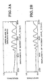
- Figures 2 and 3 show the resultant theoretical and experimental reflectance versus wavelength, from silicon nitride processed with "large” and “small” SiH 4 -to-NH 3 ratios.
- the measured refractive indices of "large” and “small” ratio films are, respectively, 2.14 and 1.93.
- the corresponding measured thicknesses of the films are, respectively; 765 nm and 770 nm. Values of various other parameters used for the simulation are given in the Figures' captions. These values yielded the excellent fit between experimental and theoretical spectra shown in the Figures.
- Transmittance of these films can be calculated based on the knowledge of their optical constants. Calculations demonstrated that only a slight percentage of excess silicon in stoichiometric silicon nitride would decrease transmittance, T, by orders of magnitude.
- the results for films 1 11m thick on a quartz substrate are summarized in the table of Figure 4.
- Refractive index, n, and absorption coefficient, a for any medium depend on the energy and thereby, the wavelength of the incident radiation.
- the absorption coefficient is a strong measure of the absorptance.
- absorptance increases exponentially by a) increasing the absorption coefficient, keeping the thickness constant, and b) increasing the thickness, keeping the absorption coefficient constant.
- values of n and a for silicon nitride, as well as amorphous Si are taken from commonly known data. Values of n and a for silicon nitride with excess Si are estimated based on a simple structural model assuming mechanical mixture of silicon nitride and Si. The microstructure of plasma deposited nitride is certainly more complicated due to large amounts (20%) of hydrogen usually incorporated in the films, which tends to reduce n and a. The conclusion, however, remains the same: excess silicon in a plasma deposition reaction renders a silicon nitride layer which is opaque to UV light.
- the refractive index and energy band gap of stoichiometric silicon nitride are, respectively, 1.96 and 5.2 eV.
- the film with refractive index of 2.14 is virtually opaque to UV light.
- Plasma deposition techniques are known in the state of the art of fabrication of semiconductor integrated circuits. Therefore, the present process can be carried out with a variety of commercially available equipment. Two embodiments are described herein in detail as performed using t e Plasma Enhanced Chemical Vapor Deposition (PECVD) system manufactured by Advanced Semiconductor Materials America, Inc. (ASM), and the AMS 3300, manufactured by Applied Materials Corporation. It is to be understood that parameter variations for the process will vary due to the geometry and operating specifications of the particular plasma deposition machine used to deposit the silicon nitride film on the semiconductor substrate or device.
- PECVD Plasma Enhanced Chemical Vapor Deposition
- ASM Advanced Semiconductor Materials America, Inc.
- AMS 3300 manufactured by Applied Materials Corporation
- the ASM system was used. The following steps are those performed in accordance with the prescribed techniques recommended by the manufacturer of the system.
- the semiconductor device such as a wafer upon which EPROM circuitry has been fabricated, is loaded into the machine's reaction chamber.
- the recommended operating temperature of the chamber is 380 degrees Centigrade.
- the chamber is evacuated and the gas inlet and outlet lines are purged to clean the system of any unwanted contaminants.
- the next step is to introduce the reactants, silane and ammonia, into the chamber in order to establish a uniform flow over the wafer, establishing a contant pressure.
- the ASM operating parameters call for a flow ratio of 600 standard cubic centimeters per minute (SCCM) of silane to 4500 SCCM of ammonia, or a ratio of 2:15.
- the atmosphere of the reaction chamber is intermittently irradiated with an RF of 50 kHz to catalyze a plasma environment (by ionizing the particles of gas in the chamber, causing the decomposition of the silane), allowing it to react with the ammonia. Silicon nitride is deposited thereby upon the wafer.
- the temperature of the reaction chamber is raised to 400 degrees Centigrade. (For devices using metal interconnects other than aluminum, the temperature may be operably higher).
- the AMS 3300 system was used to deposit the silicon nitride passivation layer.
- nitrogen is used as a carrier gas for introducing the flow of silane and ammonia across the surface of the wafer upon which the silicon nitride layer is to be deposited.
- the reaction chamber temperature has an upper practical limit of 350 degrees Centigrade.
- the carrier gas is used to improve the uniformity of the deposited layer. With the pure nitrogen present, the ratio of silane-to-ammonia is lowered from the recommended 16:21 to 7:21 and the flow of nitrogen is increased by approximately 11%. By doing so, a silicon nitride film having an index of refraction of 1.93 ⁇ 0.03 is achieved.
- An acceptable thickness for silicon nitride passivation layers is approximately one micron. Deposition rates also vary with machine geometries. For example, the ASM system has a deposition rate of 25 nm per minute. The plasma deposition must be carried on for at least 40 minutes to obtain an acceptable layer. Thicker layers can be deposited by lengthening the reaction times.
- the ratio of silane-to-ammonia must be carefully adjusted and the temperature raised sufficiently so that silicon in excess of the level which exists in stoichiometrically pure silicon nitride is minimized in order for the layer formed to be transparent to ultraviolet light.
- An EPROM having a superior passivation layer of silicon nitride can be thusly fabricated.
- Ultraviolet light transparent silicon nitride films deposited in accordance with the above- described techniques allow erasure of an EPROM within three to thirty minutes.
Landscapes
- Engineering & Computer Science (AREA)
- Chemical & Material Sciences (AREA)
- Microelectronics & Electronic Packaging (AREA)
- Power Engineering (AREA)
- Physics & Mathematics (AREA)
- Condensed Matter Physics & Semiconductors (AREA)
- General Physics & Mathematics (AREA)
- Computer Hardware Design (AREA)
- Manufacturing & Machinery (AREA)
- Chemical Kinetics & Catalysis (AREA)
- Metallurgy (AREA)
- Ceramic Engineering (AREA)
- Inorganic Chemistry (AREA)
- General Chemical & Material Sciences (AREA)
- Materials Engineering (AREA)
- Mechanical Engineering (AREA)
- Organic Chemistry (AREA)
- Plasma & Fusion (AREA)
- Formation Of Insulating Films (AREA)
- Chemical Vapour Deposition (AREA)
- Bipolar Transistors (AREA)
- Non-Volatile Memory (AREA)
- Element Separation (AREA)
Priority Applications (1)
| Application Number | Priority Date | Filing Date | Title |
|---|---|---|---|
| AT85309262T ATE55510T1 (de) | 1984-12-21 | 1985-12-19 | Siliciumnitridfilme fuer integrierte schaltungen. |
Applications Claiming Priority (2)
| Application Number | Priority Date | Filing Date | Title |
|---|---|---|---|
| US684516 | 1984-12-21 | ||
| US06/684,516 US4618541A (en) | 1984-12-21 | 1984-12-21 | Method of forming a silicon nitride film transparent to ultraviolet radiation and resulting article |
Publications (3)
| Publication Number | Publication Date |
|---|---|
| EP0186443A2 EP0186443A2 (en) | 1986-07-02 |
| EP0186443A3 EP0186443A3 (en) | 1988-09-14 |
| EP0186443B1 true EP0186443B1 (en) | 1990-08-08 |
Family
ID=24748354
Family Applications (1)
| Application Number | Title | Priority Date | Filing Date |
|---|---|---|---|
| EP85309262A Expired - Lifetime EP0186443B1 (en) | 1984-12-21 | 1985-12-19 | Silicon nitride films for integrated circuits |
Country Status (5)
| Country | Link |
|---|---|
| US (1) | US4618541A (ja) |
| EP (1) | EP0186443B1 (ja) |
| JP (1) | JP2630355B2 (ja) |
| AT (1) | ATE55510T1 (ja) |
| DE (1) | DE3579137D1 (ja) |
Families Citing this family (52)
| Publication number | Priority date | Publication date | Assignee | Title |
|---|---|---|---|---|
| FR2580864B1 (fr) * | 1984-12-18 | 1987-05-22 | Thomson Csf | Couche barriere au bombardement ionique pour tube a vide |
| US4786864A (en) * | 1985-03-29 | 1988-11-22 | International Business Machines Corporation | Photon assisted tunneling testing of passivated integrated circuits |
| US4761332A (en) * | 1985-06-24 | 1988-08-02 | International Business Machines Corporation | Planarized ceramic substrates |
| US5010024A (en) * | 1987-03-04 | 1991-04-23 | Advanced Micro Devices, Inc. | Passivation for integrated circuit structures |
| EP0281324B1 (en) * | 1987-03-04 | 2000-07-19 | Advanced Micro Devices, Inc. | Improved passivation for integrated circuit structures |
| JP2551595B2 (ja) * | 1987-07-31 | 1996-11-06 | 工業技術院長 | 半導体不揮発性メモリ素子 |
| US5020030A (en) * | 1988-10-31 | 1991-05-28 | Huber Robert J | Nonvolatile SNOS memory cell with induced capacitor |
| JPH0645893B2 (ja) * | 1989-02-17 | 1994-06-15 | 科学技術庁長官官房会計課長 | 薄膜の形成方法 |
| US4951063A (en) * | 1989-05-22 | 1990-08-21 | Xerox Corporation | Heating elements for thermal ink jet devices |
| EP0408054A3 (en) * | 1989-07-14 | 1991-10-30 | Kabushiki Kaisha Toshiba | Ultraviolet erasable non-volatile semiconductor memory apparatus |
| US5041888A (en) * | 1989-09-18 | 1991-08-20 | General Electric Company | Insulator structure for amorphous silicon thin-film transistors |
| DE4013306A1 (de) * | 1990-04-26 | 1991-10-31 | Hoechst Ag | Optische formkoerper aus siliziumnitrid, sowie verfahren zu deren herstellung |
| FR2666324B1 (fr) * | 1990-09-03 | 1993-04-09 | Saint Gobain Vitrage Int | Couches minces de nitrure de silicium a proprietes ameliorees. |
| EP0484916A3 (en) * | 1990-11-07 | 1993-06-02 | Sumitomo Electric Industries, Limited | Silicon nitride sintered body |
| JP2667605B2 (ja) * | 1991-02-21 | 1997-10-27 | 株式会社東芝 | 不揮発性半導体記憶装置およびその製造方法 |
| US5260236A (en) * | 1991-06-07 | 1993-11-09 | Intel Corporation | UV transparent oxynitride deposition in single wafer PECVD system |
| JP2791525B2 (ja) * | 1992-04-16 | 1998-08-27 | 三菱電機株式会社 | 反射防止膜の選定方法およびその方法により選定された反射防止膜 |
| JP3632256B2 (ja) * | 1994-09-30 | 2005-03-23 | 株式会社デンソー | 窒化シリコン膜を有する半導体装置の製造方法 |
| US5578517A (en) * | 1994-10-24 | 1996-11-26 | Taiwan Semiconductor Manufacturing Company Ltd. | Method of forming a highly transparent silicon rich nitride protective layer for a fuse window |
| EP0738424B1 (en) * | 1994-11-07 | 2010-05-19 | Macronix International Co., Ltd. | Integrated circuit passivation process |
| US5780891A (en) | 1994-12-05 | 1998-07-14 | Micron Technology, Inc. | Nonvolatile floating gate memory with improved interploy dielectric |
| US5728453A (en) * | 1995-12-28 | 1998-03-17 | Advanced Micro Devices, Inc. | Method of fabricating topside structure of a semiconductor device |
| US6207994B1 (en) * | 1996-11-05 | 2001-03-27 | Power Integrations, Inc. | High-voltage transistor with multi-layer conduction region |
| US6639277B2 (en) | 1996-11-05 | 2003-10-28 | Power Integrations, Inc. | High-voltage transistor with multi-layer conduction region |
| US6168983B1 (en) | 1996-11-05 | 2001-01-02 | Power Integrations, Inc. | Method of making a high-voltage transistor with multiple lateral conduction layers |
| US6566281B1 (en) * | 1997-10-15 | 2003-05-20 | International Business Machines Corporation | Nitrogen-rich barrier layer and structures formed |
| US6166439A (en) * | 1997-12-30 | 2000-12-26 | Advanced Micro Devices, Inc. | Low dielectric constant material and method of application to isolate conductive lines |
| US6768171B2 (en) | 2000-11-27 | 2004-07-27 | Power Integrations, Inc. | High-voltage transistor with JFET conduction channels |
| US6509220B2 (en) | 2000-11-27 | 2003-01-21 | Power Integrations, Inc. | Method of fabricating a high-voltage transistor |
| US6424007B1 (en) * | 2001-01-24 | 2002-07-23 | Power Integrations, Inc. | High-voltage transistor with buried conduction layer |
| US6573558B2 (en) * | 2001-09-07 | 2003-06-03 | Power Integrations, Inc. | High-voltage vertical transistor with a multi-layered extended drain structure |
| US6555873B2 (en) * | 2001-09-07 | 2003-04-29 | Power Integrations, Inc. | High-voltage lateral transistor with a multi-layered extended drain structure |
| US6635544B2 (en) * | 2001-09-07 | 2003-10-21 | Power Intergrations, Inc. | Method of fabricating a high-voltage transistor with a multi-layered extended drain structure |
| US7221011B2 (en) * | 2001-09-07 | 2007-05-22 | Power Integrations, Inc. | High-voltage vertical transistor with a multi-gradient drain doping profile |
| US7786533B2 (en) | 2001-09-07 | 2010-08-31 | Power Integrations, Inc. | High-voltage vertical transistor with edge termination structure |
| US6930364B2 (en) * | 2001-09-13 | 2005-08-16 | Silicon Light Machines Corporation | Microelectronic mechanical system and methods |
| US6963403B2 (en) * | 2002-01-15 | 2005-11-08 | Council Of Scientific And Industrial Research | Method for determining the reflectance profile of materials |
| DE10223954A1 (de) * | 2002-05-29 | 2003-12-11 | Infineon Technologies Ag | Plasmaangeregtes chemisches Gasphasenabscheide-Verfahren zum Abscheiden von Siliziumnitrid oder Siliziumoxinitrid, Verfahren zum Herstellen einer Schicht-Anordnung und Schicht-Anordnung |
| EP1398830A1 (en) * | 2002-09-12 | 2004-03-17 | STMicroelectronics S.r.l. | Process for the contact opening definition for the active element electric connections |
| US6924241B2 (en) * | 2003-02-24 | 2005-08-02 | Promos Technologies, Inc. | Method of making a silicon nitride film that is transmissive to ultraviolet light |
| US8420520B2 (en) * | 2006-05-18 | 2013-04-16 | Megica Corporation | Non-cyanide gold electroplating for fine-line gold traces and gold pads |
| US7468536B2 (en) | 2007-02-16 | 2008-12-23 | Power Integrations, Inc. | Gate metal routing for transistor with checkerboarded layout |
| US7557406B2 (en) | 2007-02-16 | 2009-07-07 | Power Integrations, Inc. | Segmented pillar layout for a high-voltage vertical transistor |
| US7859037B2 (en) * | 2007-02-16 | 2010-12-28 | Power Integrations, Inc. | Checkerboarded high-voltage vertical transistor layout |
| US8653583B2 (en) | 2007-02-16 | 2014-02-18 | Power Integrations, Inc. | Sensing FET integrated with a high-voltage transistor |
| US7595523B2 (en) | 2007-02-16 | 2009-09-29 | Power Integrations, Inc. | Gate pullback at ends of high-voltage vertical transistor structure |
| US8563095B2 (en) * | 2010-03-15 | 2013-10-22 | Applied Materials, Inc. | Silicon nitride passivation layer for covering high aspect ratio features |
| US9660053B2 (en) | 2013-07-12 | 2017-05-23 | Power Integrations, Inc. | High-voltage field-effect transistor having multiple implanted layers |
| US10325988B2 (en) | 2013-12-13 | 2019-06-18 | Power Integrations, Inc. | Vertical transistor device structure with cylindrically-shaped field plates |
| US9543396B2 (en) | 2013-12-13 | 2017-01-10 | Power Integrations, Inc. | Vertical transistor device structure with cylindrically-shaped regions |
| US20160023242A1 (en) * | 2014-07-28 | 2016-01-28 | Osram Sylvania Inc. | Method of making wavelength converters for solid state lighting applications |
| JP7076971B2 (ja) * | 2017-09-28 | 2022-05-30 | キヤノン株式会社 | 撮像装置およびその製造方法ならびに機器 |
Family Cites Families (6)
| Publication number | Priority date | Publication date | Assignee | Title |
|---|---|---|---|---|
| JPS5432509B2 (ja) * | 1972-06-02 | 1979-10-15 | ||
| JPS5244795A (en) * | 1975-10-08 | 1977-04-08 | Hitachi Ltd | Formation of silicon nitride film |
| SE7700229L (sv) * | 1976-01-22 | 1977-07-23 | Western Electric Co | Forfarande for beleggning av substrat genom utfellning fran ett plasma |
| US4181751A (en) * | 1978-05-24 | 1980-01-01 | Hughes Aircraft Company | Process for the preparation of low temperature silicon nitride films by photochemical vapor deposition |
| JPS554918A (en) * | 1978-06-26 | 1980-01-14 | Hitachi Ltd | Passivation film structure and manufacturing method thereof |
| JPS56149306A (en) * | 1980-04-21 | 1981-11-19 | Kokusai Electric Co Ltd | Formation of silicon nitride film |
-
1984
- 1984-12-21 US US06/684,516 patent/US4618541A/en not_active Expired - Lifetime
-
1985
- 1985-12-19 DE DE8585309262T patent/DE3579137D1/de not_active Expired - Lifetime
- 1985-12-19 AT AT85309262T patent/ATE55510T1/de not_active IP Right Cessation
- 1985-12-19 EP EP85309262A patent/EP0186443B1/en not_active Expired - Lifetime
- 1985-12-20 JP JP60289137A patent/JP2630355B2/ja not_active Expired - Lifetime
Also Published As
| Publication number | Publication date |
|---|---|
| JP2630355B2 (ja) | 1997-07-16 |
| EP0186443A2 (en) | 1986-07-02 |
| US4618541A (en) | 1986-10-21 |
| DE3579137D1 (de) | 1990-09-13 |
| JPS61159576A (ja) | 1986-07-19 |
| ATE55510T1 (de) | 1990-08-15 |
| EP0186443A3 (en) | 1988-09-14 |
Similar Documents
| Publication | Publication Date | Title |
|---|---|---|
| EP0186443B1 (en) | Silicon nitride films for integrated circuits | |
| US4581622A (en) | UV erasable EPROM with UV transparent silicon oxynitride coating | |
| US6395650B1 (en) | Methods for forming metal oxide layers with enhanced purity | |
| US4371587A (en) | Low temperature process for depositing oxide layers by photochemical vapor deposition | |
| EP1340247B1 (en) | Method of forming dielectric films | |
| Ito et al. | Very thin silicon nitride films grown by direct thermal reaction with nitrogen | |
| EP0030798A1 (en) | Low temperature process for depositing oxide layers by photochemical vapor deposition | |
| JPS60258915A (ja) | レ−ザ−化学気相沈積方法および装置 | |
| US6924241B2 (en) | Method of making a silicon nitride film that is transmissive to ultraviolet light | |
| US6531714B1 (en) | Process for the production of a semiconductor device having better interface adhesion between dielectric layers | |
| Katz et al. | Properties of titanium nitride thin films deposited by rapid‐thermal‐low‐pressure‐metalorganic‐chemical‐vapor‐deposition technique using tetrakis (dimethylamido) titanium precursor | |
| US20030003243A1 (en) | Method for forming film | |
| KR20040026147A (ko) | 절연막 형성방법, 반도체장치 및 제조장치 | |
| Bergonzo et al. | Low pressure photodeposition of silicon nitride films using a xenon excimer lamp | |
| US6906365B2 (en) | Ferroelectric memory device including an upper protection electrode | |
| Stein | Hydrogen content and annealing of memory quality silicon-oxynitride films | |
| Rojas et al. | Characterization of silicon dioxide and phosphosilicate glass deposited films | |
| Nguyen et al. | Plasma deposition and characterization of thin silicon‐rich silicon nitride films | |
| US6037614A (en) | Methods for manufacturing group IV element alloy semiconductor materials and devices that include such materials | |
| Lee et al. | The preparation, characterization and application of plasma-enhanced chemically vapour deposited silicon nitride films deposited at low temperatures | |
| Inada et al. | Chemical vapor deposition of silicon nitride: encapsulant layers for annealing gallium arsenide | |
| Gritsenko et al. | Study of Excess Silicon at Si3 N 4/Thermal SiO2 Interface Using EELS and Ellipsometric Measurements | |
| Shibagaki et al. | Low temperature silicon nitride deposition using microwave-excited active nitrogen | |
| Logothetidis et al. | In-situ and real time room temperature oxidation studies of fcc TiN thin films | |
| Jun et al. | Composition, oxidation, and optical properties of fluorinated silicon nitride film by inductively coupled plasma enhanced chemical vapor deposition |
Legal Events
| Date | Code | Title | Description |
|---|---|---|---|
| PUAI | Public reference made under article 153(3) epc to a published international application that has entered the european phase |
Free format text: ORIGINAL CODE: 0009012 |
|
| AK | Designated contracting states |
Kind code of ref document: A2 Designated state(s): AT BE CH DE FR GB IT LI LU NL SE |
|
| PUAL | Search report despatched |
Free format text: ORIGINAL CODE: 0009013 |
|
| AK | Designated contracting states |
Kind code of ref document: A3 Designated state(s): AT BE CH DE FR GB IT LI LU NL SE |
|
| 17P | Request for examination filed |
Effective date: 19881029 |
|
| 17Q | First examination report despatched |
Effective date: 19890210 |
|
| GRAA | (expected) grant |
Free format text: ORIGINAL CODE: 0009210 |
|
| AK | Designated contracting states |
Kind code of ref document: B1 Designated state(s): AT BE CH DE FR GB IT LI LU NL SE |
|
| PG25 | Lapsed in a contracting state [announced via postgrant information from national office to epo] |
Ref country code: SE Free format text: THE PATENT HAS BEEN ANNULLED BY A DECISION OF A NATIONAL AUTHORITY Effective date: 19900808 Ref country code: NL Effective date: 19900808 Ref country code: LI Effective date: 19900808 Ref country code: IT Free format text: LAPSE BECAUSE OF FAILURE TO SUBMIT A TRANSLATION OF THE DESCRIPTION OR TO PAY THE FEE WITHIN THE PRESCRIBED TIME-LIMIT;WARNING: LAPSES OF ITALIAN PATENTS WITH EFFECTIVE DATE BEFORE 2007 MAY HAVE OCCURRED AT ANY TIME BEFORE 2007. THE CORRECT EFFECTIVE DATE MAY BE DIFFERENT FROM THE ONE RECORDED. Effective date: 19900808 Ref country code: FR Effective date: 19900808 Ref country code: CH Effective date: 19900808 Ref country code: BE Effective date: 19900808 Ref country code: AT Effective date: 19900808 |
|
| REF | Corresponds to: |
Ref document number: 55510 Country of ref document: AT Date of ref document: 19900815 Kind code of ref document: T |
|
| REF | Corresponds to: |
Ref document number: 3579137 Country of ref document: DE Date of ref document: 19900913 |
|
| REG | Reference to a national code |
Ref country code: CH Ref legal event code: PL |
|
| PG25 | Lapsed in a contracting state [announced via postgrant information from national office to epo] |
Ref country code: GB Effective date: 19901219 |
|
| EN | Fr: translation not filed | ||
| PG25 | Lapsed in a contracting state [announced via postgrant information from national office to epo] |
Ref country code: LU Free format text: LAPSE BECAUSE OF NON-PAYMENT OF DUE FEES Effective date: 19901231 |
|
| NLV1 | Nl: lapsed or annulled due to failure to fulfill the requirements of art. 29p and 29m of the patents act | ||
| PLBE | No opposition filed within time limit |
Free format text: ORIGINAL CODE: 0009261 |
|
| STAA | Information on the status of an ep patent application or granted ep patent |
Free format text: STATUS: NO OPPOSITION FILED WITHIN TIME LIMIT |
|
| 26N | No opposition filed | ||
| GBPC | Gb: european patent ceased through non-payment of renewal fee | ||
| PG25 | Lapsed in a contracting state [announced via postgrant information from national office to epo] |
Ref country code: DE Effective date: 19910903 |