EP0185411B1 - Schaltvorrichtung zur Unterdrückung eines Signals - Google Patents
Schaltvorrichtung zur Unterdrückung eines Signals Download PDFInfo
- Publication number
- EP0185411B1 EP0185411B1 EP85201915A EP85201915A EP0185411B1 EP 0185411 B1 EP0185411 B1 EP 0185411B1 EP 85201915 A EP85201915 A EP 85201915A EP 85201915 A EP85201915 A EP 85201915A EP 0185411 B1 EP0185411 B1 EP 0185411B1
- Authority
- EP
- European Patent Office
- Prior art keywords
- output
- amplifier
- input
- differential amplifier
- current
- Prior art date
- Legal status (The legal status is an assumption and is not a legal conclusion. Google has not performed a legal analysis and makes no representation as to the accuracy of the status listed.)
- Expired - Lifetime
Links
Images


Classifications
-
- H—ELECTRICITY
- H03—ELECTRONIC CIRCUITRY
- H03K—PULSE TECHNIQUE
- H03K17/00—Electronic switching or gating, i.e. not by contact-making and –breaking
- H03K17/51—Electronic switching or gating, i.e. not by contact-making and –breaking characterised by the components used
- H03K17/56—Electronic switching or gating, i.e. not by contact-making and –breaking characterised by the components used by the use, as active elements, of semiconductor devices
- H03K17/60—Electronic switching or gating, i.e. not by contact-making and –breaking characterised by the components used by the use, as active elements, of semiconductor devices the devices being bipolar transistors
-
- H—ELECTRICITY
- H03—ELECTRONIC CIRCUITRY
- H03F—AMPLIFIERS
- H03F3/00—Amplifiers with only discharge tubes or only semiconductor devices as amplifying elements
- H03F3/72—Gated amplifiers, i.e. amplifiers which are rendered operative or inoperative by means of a control signal
-
- H—ELECTRICITY
- H03—ELECTRONIC CIRCUITRY
- H03G—CONTROL OF AMPLIFICATION
- H03G3/00—Gain control in amplifiers or frequency changers without distortion of the input signal
- H03G3/20—Automatic control
- H03G3/30—Automatic control in amplifiers having semiconductor devices
- H03G3/34—Muting amplifier when no signal is present or when only weak signals are present, or caused by the presence of noise signals, e.g. squelch systems
- H03G3/348—Muting in response to a mechanical action or to power supply variations, e.g. during tuning; Click removal circuits
Definitions
- the invention relates to a switching device for suppressing a signal, comprising:
- Such a switching device is disclosed in United States Patent Specification US-A-4,315,221.
- the device described therein is constituted by a differential amplifier which is arranged as a voltage follower and whose output drives an output stage comprising two complementary output transistors arranged as emitter followers.
- These output transistors are operated in class AB by means of a bias circuit comprising two diodes and two current sources included in a switchable current mirror.
- the signal to the output of the output stage is suppressed by switching off the current mirror and hence the quiescent current of the output stage.
- a drawback of this circuit is that in the switched-off condition the input signal is present on the input of the output stage, so that the signal may still appear on the output of the output stage as a result of crosstalk.
- Another drawback is that in the switched-on condition the output signal may be distorted as a result of the non-linear resistance of the output transistors.
- United States Patent Specification US-A-4.,366,442 discloses a switching device of the type defined in the opening paragraph, which also comprises a differential amplifier whose output drives a class AB output stage by means of two diodes and a current source.
- the output stage in this switching device comprises two parallel branches each comprising two complementary output transistors. The output of the first branch is fed back to an input of the differential amplifier and the output of the second branch constitutes the output of the switching device. The signal to this output is suppressed by switching off the current sources of the differential amplifier and the output stage.
- This arrangement also has the drawback that the output signal may be distorted in the switched-on condition.
- the output transistors of the first branch produce hardly any distortion owing to the feedback, but unless they are loaded in the same way as the output transistors of the first branch the output transistors of the second branch will give rise to distortion. However, in general these transistors are not loaded in the same way.
- the invention is based on the recognition of the following facts.
- the switched-on condition the output of the output stage is fully fed back to the second input of the first differential amplifier, so that the switching device operates as a voltage follower.
- This negative feedback leads to a substantial reduction of the distortion produced by the non-linear resistance of the output transistors, so that the input signal appears substantially undistorted on the output.
- the switched-off condition the first differential amplifier and the output amplifier are currentless, whilst a second differential amplifier is switched on. The first input of the latter is connected to earth and its output is fully fed back to the second input, so that this differential amplifier operates as a voltage follower. Then there is no signal on the input of the output amplifier in the switched-off condition, so that the input signal is suppressed almost completely and the occurrence of cross-talk is precluded.
- An advantageous embodiment of the invention is characterized in that the first current source and the third current source are replaced by a current source which is common to the first differential amplifier and the second differential amplifier and which is switchable from the first differential amplifier to the second differential amplifier and vice versa, and the first conversion circuit and the second conversion circuit are replaced by a conversion circuit which is common to the first differential amplifier and the second differential amplifier.
- a further embodiment may be characterized in that the output of the conversion circuit is connected to the input of a driver amplifier having an output coupled to the input of the output amplifier.
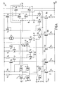
- Fig. 1 is the basic diagram of a switching device in accordance with the invention.
- the switching device comprises a first input amplifier 1 having a non-inverting input 2, to which an input signal v, may be applied, and an inverting input 3.
- the input amplifier 1 comprises a differential amplifier, not shown for the sake of clarity, whose bias current is furnished by a current source 4 which can be disconnected by means of a switch 5.
- the output 6 of the amplifier 1 is connected to the input 7 of an output amplifier 8.
- the output 9 of this amplifier 8 constitutes the output of the switching device and is connected to the inverting input 3 of the input amplifier 1.
- the output amplifier 8 receives a bias current which is supplied by at least one current source 10, which can be disconnected by means of a switch 11.
- the switching device comprises a second input amplifier 12 having a non-inverting input 13 which is earthed for signals, and an inverting input 14.
- the output 15 of this amplifier 12 is connected to the inverting input 14 and to the input 7 of the output amplifier 8.
- the second input amplifier 12 also comprises a differential amplifier, not shown, whose bias current is furnished by a current source 16 which can be switched on by means of a switch 17.
- the switches 5, 11 and 17 are energised by control means, not shown, in such a way that the switches 5 and 11 are closed simultaneously and at the same time the switch 17 is opened, and vice versa.
- the switching device operates as follows. In the switched-on condition of the switching device the switches 5 and 11 are closed and the switch 17 is consequently open.
- the first input amplifier 1 and the output amplifier 8 are powered by the current sources 4 and 10. Owing to full negative feedback from the output 9 of the output amplifier 8 to the inverting input 3 of the first input amplifier 1 the switching device operates as a voltage follower.
- the distortion, which is mainly caused by the output amplifier 8 is reduced substantially by this negative feedback, so that the substantially undistorted input voltage v, appears on the output 9.
- the switches 5 and 11 are open and the switch 17 is closed, so that now only the second input amplifier 12 is operative.
- this input amplifier 12 operates as a voltage follower.
- the voltage on the output 15 and hence on the input 7 of the output amplifier is therefore 0 V.
- no signal appears on the input 7 of the output amplifier 8 the signal cannot appear on the output 9 as a result of crosstalk.
- the first differential amplifier 1 and the second differential amplifier 12 have equal loads, which may be followed by identical driver amplifiers.
- the basic arrangement shown in Fig. 1 may be simplified by combining the two loads into one common load and the driver amplifiers into one common driver amplifier.
- Fig. 2 shows this simplified arrangement, in which the common load and, as the case may be, the common driver amplifier bear the reference numeral 20.
- the current sources 4 and 16 may be combined to form one current source 21 which can be switched from differential amplifier 1 to differential amplifier 12 and vice versa by means of one switch 22. Otherwise the circuit operates in the same way as that shown in Fig. 1.
- the first differential amplifier 1 comprises two transistors T, and T 2 , the base 2 of the transistor T, constituting the non-inverting input to which an input signal v, is applied, and the base 3 of transistor T 2 constituting the inverting input.
- the collector of transistor T is connected to an input of a current mirror 20, which comprises a diode-connected transistor T 8 and a transistor Tg and which has its output connected to the collector of transistor T 2 and to the output 6 of the differential amplifier.
- the current mirror 20 constitutes a conversion circuit by means of which the differential collector currents of the transistors T 1 and T 2 are converted into a single-ended output current.
- the second differential amplifier 12 comprises two transistors T 3 and T 4 , the base 13 of the transistor T 3 being connected to earth and constituting the non-inverting input.
- the collector of transistor T 3 and the collector of transistor T 4 are connected to the collector of transistor T 1 and the collector of transistor T 2 , respectively, so that the current mirror 20 constitutes a conversion circuit which is common to the two differential amplifiers 1 and 12.
- the base 14 of transistor T 4 constitutes the inverting input of the differential amplifier 12 and is connected to the output 6 of this amplifier.
- the emitter currents of the differential amplifiers 1 and 12 are furnished by a current source 21 which comprises a transistor T 7 whose base is at a reference voltage V ref and whose emitter is connected to the negative power-supply line 30 by means of a resistor R 1 .
- the current from the current source 21 can be switched from one differential amplifier to the other by means of a switch 22 comprising two transistors T 5 and T 6 arranged as a differential pair, the control signals for this change-over being applied to the base 33 of the transistor T 5 and the base 34 of the transistor T 6 , respectively.
- the common output 6 of the two differential amplifiers 1 and 12 is connected to the input 7 of an output amplifier 8 comprising two complementary output transistors T 10 and T 11 arranged as an emitter followers, the common emitter terminal constituting the output 9 of the switching device.
- the base of the transistor T 11 is connected to the emitter of a transistor T 13 , whose base is connected to the input 7 of the output amplifier 8 and whose collector is connected to the positive power-supply terminal 31.
- the emitter of the transistor T 13 can be connected to a current source 10a by means of a switch 11a, which current source comprises a transistor T 16 whose base is at a reference voltage and whose emitter is connected to the negative power-supply terminal 30 via a resistor R 2 .
- the switch 11 a comprises two transistors T 14 and T 15 arranged as a differential pair, the collector of the transistor T 14 being connected to the emitter of the transistor T 13 and the collector of the transistor T 15 being connected to the positive power-supply terminal 31.
- the control signals applied to the bases of the transistors T 14 and T 15 are the same as those applied to the bases 33 and 34 of the transistors T 5 and T 6 .
- the base of transistor T 10 is connected to the emitter of a transistor T 12 , whose base is connected to the input 7 and whose collector is connected to the negative power-supply terminal 30.
- the emitter of the transistor T 12 is connected to the output of a current mirror comprising a diode-connected transistor T 20 and transistor T 21 , whose base-emitter junction is arranged in parallel with that of the transistor T 20 .
- the input of the current mirror may be connected to a current source 10b by means of a switch 11b, which current source comprises a transistor T 19 whose base is at a reference voltage and whose emitter is connected to the negative power-supply terminal 30 via a resistor R 3 .
- the switch 11 b comprises two transistors T 17 and T 18 arranged as a differential pair, the collector of the transistor T 17 being connected to the input of the current mirror T 20 , T 21 and the collector of the transistor T 18 being connected to the positive power-supply terminal 31.
- the base of the transistor T 17 is connected to the base 33 of the transistor T s and the base of the transistor T 18 is connected to the base 34 of the transistor T 6 .
- the bases 33 and 34 receive such control signals that the voltage on the base 33 of the transistor T 5 is high relative to the voltage on the base 34 of the transistor T s .
- the transistor T s is turned on and the transistor T 6 is turned off.
- the current source 21 is connected to the differential amplifier 1 and the differential amplifier 12 is disconnected.
- the transistor T 14 conducts and the transistor T, 5 is cut off, so that the current source 10a is connected to the emitter of the transistor T 13 .
- the current source 10b is connected to the emitter of the transistor T 12 via the conductive transistor T 17 and the current mirror T 2O , T 21 .
- the conducting transistors T 12 and T 13 ensure that a voltage equal to two base-emitter voltages appears between the bases of the transistors T 10 and T 11 . As a result of this voltage a small quiescent current will flow in the output transistors T 10 and T 11 , so that the output amplifier 8 is operated in class AB.
- the combination of the differential amplifier and the output amplifier 8 will behave as a voltage follower in the switched-on condition. Therefore, the voltage on the output 9 is substantially equal to the voltage on the input 2 and the harmonic distortion of the output signal as a result of the non-linearity of the resistances of the output transistors T 10 and T 11 is reduced substantially by the negative feedback.
- the voltage on the base 34 of the transistor T 6 is high relative to the voltage on the base of the transistor T 5 , so that the transistor T 6 is turned on and the transistor T 5 is cut off.
- the current source 21 is connected to the commoned emitters of the transistors T 3 and T 4 via the transistor T 6 , so that now the differential amplifier 12 is switched on and the differential amplifier 1 is turned off.
- the voltages on the bases of the transistors T 18 and T 15 are now also high relative to the voltages on the bases of the transistors T1 7 and T 14 , so that the transistors T 18 and T 15 conduct and the transistors T 14 and T 17 are cut off.
- the current sources 10a and 10b are connected to the positive power-supply terminal 31, so that the output amplifier 8 is currentless.
- the output 9 of the output amplifier 8 then has a high impedance.
- the differential amplifier 12 will behave as a voltage follower.
- the voltage on the output 6 and hence on the input 7 of the output amplifier 8 is then 0 V. Therefore, no signal will appear on the input 7 of the output amplifier 8 in the switched-off condition, so that a very good suppression of the input signal is obtained.
- the transistors of the differential amplifiers 1 and 2 may alternatively be PNP transistors, in which case the transistors of the current mirror 20 should be NPN transistors.
- the input of the current mirror should then be connected to the collector of the transistor T 2 and the output of the current mirror should be connected to the collector of the transistor T 1 .
- Further other current mirror may be used instead of the current mirror shown.
- the collectors of the transistors T 12 and T 13 may be connected to the base of the relevant transistor instead of to the negative power-supply terminal and the positive power-supply terminal, so that the transistors T 12 and T 13 are then connected as diodes.
- FIG. 4 A switching device in accordance with a second embodiment will now be described in more detail with reference to Fig. 4, in which identical parts bear the same reference numerals as in Fig. 3.
- the interconnected collectors of the transistors T 1 and T 3 and the interconnected collectors of the transistors T 2 and T 4 are not connected to the input and to the output of a current mirror, respectively, but are connected to the positive power-supply terminal 31 by means of a resistor R 4 and an identical resistor R 5 , respectively.
- the voltages across the resistors R 4 and R 5 are applied to the base of a transistor T 23 , which is operated as an emitter follower by means of a current source 35, and to the base of a transistor T 24 , which is operated as an emitter follower by means of a current source 36, respectively.
- the current sources 35 and 36 comprise transistors T 25 and T 26 whose bases are at a reference voltage and whose emitters are connected to the negative power-supply terminal 30 by a resistor R 8 and a resistor R 9 , respectively.
- the emitter of the transistor T 23 is connected to the base of a transistor T 27 , whose emitter is connected to the positive power-supply terminal 31 by a resistor R 6 .
- the emitter of the transistor T 24 is connected to the base of a transistor T 28 having a resistor R 7 arranged in the emitter line.
- the collector of the transistor T 27 is connected to the collector of the transistor T 28 by a current mirror comprising a diode-connected transistor T 29 and a transistor T 30 whose base-emitter junction is arranged in parallel with that of the transistor T 29 .
- the transistors T 23 to T 30 with the resistors R 4 to R 7 constitute a conversion circuit for converting the collector currents of the transistors T 1 and T 2 into a single-ended output current.
- the collector current of the transistor T 1 is converted into a voltage by means of resistor R 4 , which voltage is applied to the voltage-to-current converter.
- T 27 , R o via the emitter follower T 23 and the current source 35.
- the collector current of the transistor T 27 is consequently inverted relative to the collector current of the transistor T 1 .
- the collector current of the transistor T 28 is inverted relative to the collector current or the transistor T 2 .
- the output current of the current mirror T 29 , T 30 is inverted relative to the output current of the current mirror 20 in the embodiment shown in Fig. 3, which is necessary in view of the inverting driver amplifier used in the circuit shown in Fig. 4.
- the collector of the transistor T 28 is connected to the input 41 of this driver amplifier 40, which comprises two transistors T 4 , and T 42 in Darlington arrangement, the collector of the transistor T 41 being connected to the positive power-supply terminal 31 and the collector of the transistor T 42 being connected to a current source 37.
- the collector of the transistor T 42 constitutes the common output 6 of the first input amplifier and the second input amplifier.
- a capacitor C 1 is arranged between the output 6 and the input 41 of the driver amplifier 40.
- the output 6 is connected to the inverting input 14 of the second differential amplifier 12 and to the input 7 of the output amplifier 8, which is of the same construction as that shown in Fig. 3.
- the driver amplifier 40 provides an additional amplification of the signal from the differential amplifiers.
- the circuit operates in the same way as that in Fig. 3. In the switched-on condition the differential amplifier 1 together with the driver amplifier 40 and the output amplifier 8 are driven and the negative feedback between the output 9 and the inverting input 3 ensures that the voltage on the output 9 is substantially identical to the voltage on input 2. In the switched-off condition the second differential amplifier 12 together with the driver amplifier 40 is driven.
- the first differential amplifier 1 and the second differential amplifier 12 may comprise PNP transistors in which case the collectors of the transistors T 1 and T 2 should be connected to the input and the output, respectively, of a current mirror, the input of the driver amplifier being driven directly by the output.
- a switching device in accordance with a third embodiment will be described with reference to Fig. 5, in which identical parts bear the same reference numerals as in Fig. 4.
- the circuit Up to the common driver amplifier the circuit is identical to that shown in Fig. 4.
- the output amplifier 8 differs from that shown in Fig. 4 in that the transistor T 12 is an NPN-transistor instead of a PNP-transistor and the transistor T 13 is a PNP-transistor instead of an NPN-transistor.
- the transistors T 12 and T, 3 are now arranged between the bases of the output transistors T 10 and T 11 and are connected as diodes, the emitters of these transistors being interconnected and being connected to the input 14 of the second differential amplifier 12 and to the collectors of the transistors T, 5 and T 5 ,.
- the collector of the transistor T, 3 constitutes the input 7 of the output amplifier 8 and is again connected to the collector of the transistor T 14 which together with transistor T 15 constitutes the switch 11a.
- the common emitter terminal of the transistors T 14 and T, 5 is not connected to a current source but to the output 6 of the driver amplifier 40, which is otherwise identical to the driver amplifier 40 in Fig.
- the collector of the transistor T 12 is connected to the collector of the transistor T 17 via a current mirror comprising transistors T 20 and T 2 ,, which transistor T 17 together with the transistor T, 8 constitutes a differential pair whose common emitter terminal is connected to a current source 10b, which comprises the transistor T 19 and the resistor R 3 .
- the collector of the transistor T, 8 is not connected to the positive power-supply terminal 31 but to the collector of the transistor T, 5 via a current mirror comprising the transistors T 50 and T 51 .
- the voltage on the bases of the transistor T 14 and the transistor T 17 is high relative to the voltage on the bases of the transistor T 15 and the transistor T 18 , so that the transistors T 14 and T 17 conduct and the transistors T, 5 and T 18 are cut off.
- the current from the current source 10b now flows through the diodes T 12 , T 13 via the transistor T 17 and the current mirror T 20 , T 21 .
- the current now flowing in these diodes T 12 , T, 3 is of the order of magnitude of 1 mA. If the input 41 of the driver amplifier 40 is driven as far as possible towards the level of the negative power-supply terminal, the transistor T 42 will be substantially cut off and the collector current of the transistor T 21 will flow almost entirely to the base of the transistor T 10 .
- the last- mentioned transistor is a NPN transistor whose current gain factor ⁇ 100, so that the maximum output current in the present case is of the order of magnitude of 100 mA. If the input 41 of the driver amplifier is driven as far as possible towards the level of the positive power-supply terminal 31, the transistor T 42 will be fully conductive.
- the maximum collector current of the transistor T 42 is equal to the product of the current gain factors of the NPN transistors T 4 , and T 42 and the maximum output current of the input amplifiers 1 and 2.
- the current gain factors are ⁇ 100 and the maximum output current is dictated by the output current of the current source 21, which may be of the order of magnitude of 10 ⁇ A. Consequently, the maximum collector current of the transistor T 42 is of the order of magnitude of 100 mA.
- the voltages on the bases of the transistor T, 8 and the transistor T, 5 are high relative to the voltages on the bases of the transistors T 17 and T 14 , so that the transistors T 18 and T 15 conduct and the transistors T 17 and T 14 are cut off.
- the current from the current source 10b now flows to the output 6 of the driver amplifier 40 via the current mirror T 50 , T 51 and the transistor T 15 , which driver amplifier takes up this entire current.
- the output amplifier 8 is turned off and no signal will appear on its input 7.
- the invention is not limited to the present embodiments.
- other types of switches may be used for the switches 22, 11 a and 11b shown in the Figures.
- the differential amplifiers 1 and 12 may be of different types. The same applies to the driver amplifiers 40.
- the switching device is connected to a symmetrical power supply.
- these inputs may be connected to, for example, a tapping of a voltage divider comprising two identical resistors and arranged between the positive power-supply terminal and the negative power-supply terminal.
- the switching device may also be operated with an asymmetrical power supply.
- the first inputs of the two differential amplifiers and the output of the switching device may then be connected by a resistor, in known manner, to a tapping on a series arrangement of a resistor and a capacitor arranged between the positive power-supply terminal and the negative power-supply terminal.
- the delay in coupling the output to the remainder of the circuit when the power supply is switched on should then be adapted to the time required for charging this capacitor.
Claims (8)
dadurch gekennzeichnet, daß die Schaltung außerdem enthält,
Applications Claiming Priority (2)
| Application Number | Priority Date | Filing Date | Title |
|---|---|---|---|
| NL8403819A NL8403819A (nl) | 1984-12-17 | 1984-12-17 | Schakelinrichting voor het onderdrukken van een signaal. |
| NL8403819 | 1984-12-17 |
Publications (2)
| Publication Number | Publication Date |
|---|---|
| EP0185411A1 EP0185411A1 (de) | 1986-06-25 |
| EP0185411B1 true EP0185411B1 (de) | 1990-03-14 |
Family
ID=19844919
Family Applications (1)
| Application Number | Title | Priority Date | Filing Date |
|---|---|---|---|
| EP85201915A Expired - Lifetime EP0185411B1 (de) | 1984-12-17 | 1985-11-21 | Schaltvorrichtung zur Unterdrückung eines Signals |
Country Status (7)
| Country | Link |
|---|---|
| US (1) | US4670720A (de) |
| EP (1) | EP0185411B1 (de) |
| JP (1) | JP2578096B2 (de) |
| KR (1) | KR940000940B1 (de) |
| DE (1) | DE3576621D1 (de) |
| NL (1) | NL8403819A (de) |
| SG (1) | SG120792G (de) |
Families Citing this family (11)
| Publication number | Priority date | Publication date | Assignee | Title |
|---|---|---|---|---|
| JP2547781B2 (ja) * | 1987-07-13 | 1996-10-23 | 株式会社東芝 | Btl電力増幅回路 |
| US4857861A (en) * | 1987-09-23 | 1989-08-15 | U. S. Philips Corporation | Amplifier arrangement with improved quiescent current control |
| US4972157A (en) * | 1989-07-21 | 1990-11-20 | Advanced Micro Devices, Inc. | Operational amplifier having selectable inputs |
| JP3038952B2 (ja) * | 1991-03-15 | 2000-05-08 | 日本電気株式会社 | 増幅回路 |
| US5332928A (en) * | 1992-12-10 | 1994-07-26 | Threepenny Electronics Corporation | Battery drain reducer |
| DE69406108T2 (de) * | 1994-04-15 | 1998-02-12 | St Microelectronics Srl | Niederfrequenzverstärker |
| DE19756135C1 (de) * | 1997-12-17 | 1999-08-05 | Schwerionenforsch Gmbh | Extrapolierender Diskriminator |
| EP0938186B1 (de) * | 1998-02-19 | 2003-11-12 | STMicroelectronics S.r.l. | Anschliessen einer Kapazität an einen gegenseitig exklusiv selektierten integrierten Verstärker aus einer Vielzahl von integrierten Verstärkern |
| US6316993B1 (en) * | 1999-02-22 | 2001-11-13 | Texas Instruments Incorporated | Analog circuitry for start-up glitch suppression |
| JP4853034B2 (ja) * | 2006-01-31 | 2012-01-11 | ミツミ電機株式会社 | 出力回路 |
| JP6256135B2 (ja) * | 2014-03-20 | 2018-01-10 | 株式会社デンソー | 弾性表面波センサの信号処理装置および信号処理方法 |
Family Cites Families (7)
| Publication number | Priority date | Publication date | Assignee | Title |
|---|---|---|---|---|
| JPS5574115U (de) * | 1978-11-15 | 1980-05-22 | ||
| JPS55159630A (en) * | 1979-05-30 | 1980-12-11 | Mitsubishi Electric Corp | Analog switch |
| EP0025950B1 (de) * | 1979-09-19 | 1983-06-08 | Kabushiki Kaisha Toshiba | Verstärkervorrichtung |
| JPS6221070Y2 (de) * | 1980-07-14 | 1987-05-28 | ||
| JPS6035845B2 (ja) * | 1980-09-03 | 1985-08-16 | 松下電器産業株式会社 | ミュ−ティング増幅器 |
| JPH0230902Y2 (de) * | 1981-03-02 | 1990-08-21 | ||
| JPS592433A (ja) * | 1982-06-28 | 1984-01-09 | Toshiba Corp | サンプル回路 |
-
1984
- 1984-12-17 NL NL8403819A patent/NL8403819A/nl not_active Application Discontinuation
-
1985
- 1985-11-20 US US06/799,877 patent/US4670720A/en not_active Expired - Fee Related
- 1985-11-21 DE DE8585201915T patent/DE3576621D1/de not_active Expired - Lifetime
- 1985-11-21 EP EP85201915A patent/EP0185411B1/de not_active Expired - Lifetime
- 1985-12-13 KR KR1019850009384A patent/KR940000940B1/ko not_active IP Right Cessation
- 1985-12-17 JP JP60282129A patent/JP2578096B2/ja not_active Expired - Lifetime
-
1992
- 1992-11-24 SG SG1207/92A patent/SG120792G/en unknown
Also Published As
| Publication number | Publication date |
|---|---|
| NL8403819A (nl) | 1986-07-16 |
| KR860005492A (ko) | 1986-07-23 |
| JPS61144920A (ja) | 1986-07-02 |
| KR940000940B1 (ko) | 1994-02-04 |
| JP2578096B2 (ja) | 1997-02-05 |
| DE3576621D1 (de) | 1990-04-19 |
| SG120792G (en) | 1993-01-29 |
| EP0185411A1 (de) | 1986-06-25 |
| US4670720A (en) | 1987-06-02 |
Similar Documents
| Publication | Publication Date | Title |
|---|---|---|
| US5410274A (en) | Single-ended and differential amplifiers with high feedback input impedance and low distortion | |
| EP0185411B1 (de) | Schaltvorrichtung zur Unterdrückung eines Signals | |
| US4249136A (en) | PWM Signal power amplifier | |
| US4335360A (en) | Class AB push-pull amplifiers | |
| US5448311A (en) | Tri-state video differential driver | |
| US4367419A (en) | Analog switch | |
| US4063185A (en) | Direct coupling type power amplifier circuit | |
| US4723111A (en) | Amplifier arrangement | |
| US5378938A (en) | Sample-and-hold circuit including push-pull transconductance amplifier and current mirrors for parallel feed-forward slew enhancement and error correction | |
| JPS6262084B2 (de) | ||
| US4165494A (en) | Bi-state linear amplifier | |
| JPS63287174A (ja) | テレビジョン信号増幅回路装置 | |
| US4403200A (en) | Output stage for operational amplifier | |
| EP0566334B1 (de) | Abtast- und Haltschaltkreis mit ganzem Signalmodulationsausgleich unter Verwendung von bipolaren Transistoren eines Typs | |
| JPS6038043B2 (ja) | スイツチ回路 | |
| JPH02153616A (ja) | 駆動回路 | |
| US5225791A (en) | Non-saturating complementary type unity gain amplifier | |
| EP0156411B1 (de) | Darlingtontransistoranordnung | |
| JPH0580164B2 (de) | ||
| US3936731A (en) | Amplifier with fast recovery after input signal overswing | |
| EP0750390B1 (de) | Bildröhrensteuerungsgerät | |
| EP0156410A1 (de) | Verstärkeranordnung | |
| US4453134A (en) | High voltage operational amplifier | |
| US4538116A (en) | Output stage for an operational amplifier | |
| US5023568A (en) | Combined current differencing and operational amplifier circuit |
Legal Events
| Date | Code | Title | Description |
|---|---|---|---|
| PUAI | Public reference made under article 153(3) epc to a published international application that has entered the european phase |
Free format text: ORIGINAL CODE: 0009012 |
|
| AK | Designated contracting states |
Kind code of ref document: A1 Designated state(s): BE DE FR GB IT NL |
|
| 17P | Request for examination filed |
Effective date: 19861222 |
|
| 17Q | First examination report despatched |
Effective date: 19890214 |
|
| GRAA | (expected) grant |
Free format text: ORIGINAL CODE: 0009210 |
|
| AK | Designated contracting states |
Kind code of ref document: B1 Designated state(s): BE DE FR GB IT NL |
|
| PG25 | Lapsed in a contracting state [announced via postgrant information from national office to epo] |
Ref country code: NL Effective date: 19900314 Ref country code: BE Effective date: 19900314 |
|
| REF | Corresponds to: |
Ref document number: 3576621 Country of ref document: DE Date of ref document: 19900419 |
|
| ITF | It: translation for a ep patent filed |
Owner name: ING. C. GREGORJ S.P.A. |
|
| ET | Fr: translation filed | ||
| NLV1 | Nl: lapsed or annulled due to failure to fulfill the requirements of art. 29p and 29m of the patents act | ||
| PLBE | No opposition filed within time limit |
Free format text: ORIGINAL CODE: 0009261 |
|
| STAA | Information on the status of an ep patent application or granted ep patent |
Free format text: STATUS: NO OPPOSITION FILED WITHIN TIME LIMIT |
|
| 26N | No opposition filed | ||
| ITTA | It: last paid annual fee | ||
| ITPR | It: changes in ownership of a european patent |
Owner name: CAMBIO RAGIONE SOCIALE;PHILIPS ELECTRONICS N.V. |
|
| REG | Reference to a national code |
Ref country code: FR Ref legal event code: CD |
|
| PGFP | Annual fee paid to national office [announced via postgrant information from national office to epo] |
Ref country code: GB Payment date: 19971103 Year of fee payment: 13 |
|
| PGFP | Annual fee paid to national office [announced via postgrant information from national office to epo] |
Ref country code: FR Payment date: 19971118 Year of fee payment: 13 |
|
| PGFP | Annual fee paid to national office [announced via postgrant information from national office to epo] |
Ref country code: DE Payment date: 19980123 Year of fee payment: 13 |
|
| REG | Reference to a national code |
Ref country code: FR Ref legal event code: CD |
|
| PG25 | Lapsed in a contracting state [announced via postgrant information from national office to epo] |
Ref country code: GB Free format text: LAPSE BECAUSE OF NON-PAYMENT OF DUE FEES Effective date: 19981121 |
|
| GBPC | Gb: european patent ceased through non-payment of renewal fee |
Effective date: 19981121 |
|
| PG25 | Lapsed in a contracting state [announced via postgrant information from national office to epo] |
Ref country code: FR Free format text: LAPSE BECAUSE OF NON-PAYMENT OF DUE FEES Effective date: 19990730 |
|
| REG | Reference to a national code |
Ref country code: FR Ref legal event code: ST |
|
| PG25 | Lapsed in a contracting state [announced via postgrant information from national office to epo] |
Ref country code: DE Free format text: LAPSE BECAUSE OF NON-PAYMENT OF DUE FEES Effective date: 19990901 |