EP0182971A2 - Générateur de remise à zéro de puissance marche/arrêt - Google Patents
Générateur de remise à zéro de puissance marche/arrêt Download PDFInfo
- Publication number
- EP0182971A2 EP0182971A2 EP85109367A EP85109367A EP0182971A2 EP 0182971 A2 EP0182971 A2 EP 0182971A2 EP 85109367 A EP85109367 A EP 85109367A EP 85109367 A EP85109367 A EP 85109367A EP 0182971 A2 EP0182971 A2 EP 0182971A2
- Authority
- EP
- European Patent Office
- Prior art keywords
- power supply
- voltage
- output
- differential amplifier
- power
- Prior art date
- Legal status (The legal status is an assumption and is not a legal conclusion. Google has not performed a legal analysis and makes no representation as to the accuracy of the status listed.)
- Granted
Links
- 238000012544 monitoring process Methods 0.000 claims abstract description 4
- 239000003990 capacitor Substances 0.000 claims description 25
- 230000015556 catabolic process Effects 0.000 claims description 3
- 230000003534 oscillatory effect Effects 0.000 claims 1
- 230000007704 transition Effects 0.000 claims 1
- 238000010586 diagram Methods 0.000 description 5
- 230000005764 inhibitory process Effects 0.000 description 3
- 238000000034 method Methods 0.000 description 3
- 230000009471 action Effects 0.000 description 2
- 230000006870 function Effects 0.000 description 2
- 230000004048 modification Effects 0.000 description 2
- 238000012986 modification Methods 0.000 description 2
- 208000000044 Amnesia Diseases 0.000 description 1
- 208000026139 Memory disease Diseases 0.000 description 1
- 230000003139 buffering effect Effects 0.000 description 1
- 238000006243 chemical reaction Methods 0.000 description 1
- 230000000295 complement effect Effects 0.000 description 1
- 230000008878 coupling Effects 0.000 description 1
- 238000010168 coupling process Methods 0.000 description 1
- 238000005859 coupling reaction Methods 0.000 description 1
- 230000000694 effects Effects 0.000 description 1
- 230000002401 inhibitory effect Effects 0.000 description 1
- 230000006984 memory degeneration Effects 0.000 description 1
- 208000023060 memory loss Diseases 0.000 description 1
- 238000004806 packaging method and process Methods 0.000 description 1
- 230000008569 process Effects 0.000 description 1
- 230000035945 sensitivity Effects 0.000 description 1
- 230000001052 transient effect Effects 0.000 description 1
Images
Classifications
-
- G—PHYSICS
- G06—COMPUTING; CALCULATING OR COUNTING
- G06F—ELECTRIC DIGITAL DATA PROCESSING
- G06F1/00—Details not covered by groups G06F3/00 - G06F13/00 and G06F21/00
- G06F1/24—Resetting means
-
- G—PHYSICS
- G01—MEASURING; TESTING
- G01R—MEASURING ELECTRIC VARIABLES; MEASURING MAGNETIC VARIABLES
- G01R19/00—Arrangements for measuring currents or voltages or for indicating presence or sign thereof
- G01R19/165—Indicating that current or voltage is either above or below a predetermined value or within or outside a predetermined range of values
- G01R19/16533—Indicating that current or voltage is either above or below a predetermined value or within or outside a predetermined range of values characterised by the application
- G01R19/16538—Indicating that current or voltage is either above or below a predetermined value or within or outside a predetermined range of values characterised by the application in AC or DC supplies
-
- G—PHYSICS
- G06—COMPUTING; CALCULATING OR COUNTING
- G06F—ELECTRIC DIGITAL DATA PROCESSING
- G06F1/00—Details not covered by groups G06F3/00 - G06F13/00 and G06F21/00
- G06F1/26—Power supply means, e.g. regulation thereof
- G06F1/28—Supervision thereof, e.g. detecting power-supply failure by out of limits supervision
-
- H—ELECTRICITY
- H03—ELECTRONIC CIRCUITRY
- H03K—PULSE TECHNIQUE
- H03K17/00—Electronic switching or gating, i.e. not by contact-making and –breaking
- H03K17/22—Modifications for ensuring a predetermined initial state when the supply voltage has been applied
-
- H—ELECTRICITY
- H03—ELECTRONIC CIRCUITRY
- H03K—PULSE TECHNIQUE
- H03K17/00—Electronic switching or gating, i.e. not by contact-making and –breaking
- H03K17/22—Modifications for ensuring a predetermined initial state when the supply voltage has been applied
- H03K2017/226—Modifications for ensuring a predetermined initial state when the supply voltage has been applied in bipolar transistor switches
Definitions
- the present invention relates to a power on/off reset generator for use with digital logic and computer systems, and more specifically to a device for inhibiting such systems for write protection and protecting such systems from false interface signals while power is being sequenced.
- Class 3 system When power line interruptions occur or transient conditions exist, there may be loss of data or modification of data in memory in digital data systems. Some systems have utilized battery backup to prevent memory loss, but this procedure does not protect against the effect of power surges or transients. Some military systems require control of the logic system only during turn on and turn off, referred to as Class 3 system, while others require that reset signal control be provided at all times, including the system power off condition, known as Class 4 system.
- Certain counters, registers and similar circuits in computers and other logic circuits must be initialized to a preselected state whenever the supply voltage has been below some minimum value, such as occurs when power is first turned on, or during primary power failures.
- the circuit which detects such minimum voltage levels and generates a reset signal which is utilized by the system to perform the required initialization is referred to as a Power On Reset (P.O.R.) Generator.
- An improved power on reset generator is provided in accordance with this invention, which combines a stable voltage sensor, a time delay, a Schmitt trigger and an output driver which provides a P.O.R. signal to the controlled logic system.
- the stable voltage sensor includes a precision threshold which does not require initial adjustment and is insensitive to rise time of the monitored power supply. For example, when a 5 volt Transistor-Transistor-Logic (TTL) power supply is to be monitored, it is important that the sensor be set to a threshold E T very near the minimum TTL operating point of 4.5 volts. To obtain the requires precision without requiring adjustment, a differential amplifier is used with precision bias resistors and a temperature compensated precision voltage reference zener diode.
- TTL Transistor-Transistor-Logic
- the P.O.R. signal When the power supply is off, the P.O.R. signal is LOW, referred to as a LOW-active signal.
- a portion of the supply voltage is applied to the base of the first transistor of the differential amplifier and the base of the second transistor of the differential amplifier is maintained near ground. That transistor quickly saturates.
- the time delay circuit is implemented by a timing capacitor having a discharge transistor connected across its terminals. Saturation of the differential amplifier causes the discharge transistor to discharge any charge on the capacitor.
- the timing capacitor is connected via a precision timing resistor to the power supply and will begin to charge, generating a delay ramp voltage across the capacitor.
- the zener diode is selected in accordance with the desired value of E T . Therefore, the ramp will begin when E T is reached.
- the power supply voltage continues to rise to its normal operating level.
- the delay time is selected to be in accordance with the user requirements.
- a second differential amplifier is provided to supply a temperature-stable threshold to sense the timing ramp.
- the timing ramp voltage across the timing capacitor is connected to the input transistor of the second differential amplifier.
- the input transistor drives the P.O.R. generator output transistor, which has positive feedback to the input.
- the output transistor produces positive feedback for a Schmitt trigger function. This causes a clear, sharp HIGH P.O.R. signal which is connected to the controlled system.
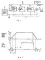
- System power supply 10 furnishes a normal operating voltage E s to the controlled system.
- the output of supply 10 is connected to stable voltage sensor 20.
- Stable voltage sensor 20 is set to respond when the power supply voltage reaches the selected threshold voltage E T , shown in Fig.3, which is the minimum for which the circuits in the controlled system are guaranteed to operate. This occurs at time t 3 .
- Sensor 20 triggers time delay circuit 30, which has a delay T selected to permit the controlled system to complete its reset process.
- time delay 30 trips Schmitt trigger 40, causing driver amplifier 50 to release the active-LOW reset signal on lead 52; note Line B of Fig.3.
- This HIGH on lead 52 enables the controlled system.
- the voltage sensor 20 resets Schmitt trigger 40, and produces the active-LOW reset signal on lead 52. It may be noted that, prior to the power supply 10 attaining the required E o voltage, the P.O.R. output on lead 52 will be uncontrolled in the interval t l , and the power supply voltage E 0 is insufficient to enable the controlled systems. This same situation occurs during turn off at t 2 .
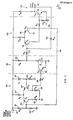
- Stable voltage sensor 20 is implemented by differential amplifier 23, 24 (Q 1 , Q 2 ), hereinafter referred to as the first differential amplifier. It will be noted that the base of Q 2 24 is returned to ground via resistor 26 (R 3 ) and to the power supply positive lead 11 by zener diode 25. The base of Q 1 23 is biased by resistors 21, 22 (R 2 , R l ). With reference to Fig.3, resistors 21, 22 and zener diode 25 (U 1 ) are selected such that the desired threshold voltage is:
- E Z is the zener (U 1 ) breakdown voltage.
- the percentage tolerance directly relates to the E T threshold tolerance.
- the zener is selected to have a precision value and the P.O.R. circuit can be built without requiring adjustable or selectable components.
- a typical example is a power supply for TTL circuits having an E S of 5 volts, which require a minimum E T voltage of 4,5.
- resistor 27 When the power supply is turned on and the power supply voltage exceeds the point designated E o , which is typically 0,7 volts, saturation of Q 2 24 occurs, causing current flow through resistor 27 (R 4 ) and resistor 28 (R 7 ) to saturate transistor 32 (Q 3 ). To ensure saturation, resistor 27 is a much smaller value than normally used for a differential amplifier.
- Transistor 32 serves as a low-impedance discharge transistor for timing capacitor 31 (C 1 ), to remove any residual charge therefrom.
- the supply continues to rise to the point when zener 25 (U 1 ) conducts. After this zener diode 25 offset, the base voltage of Q 2 24 will rise at a faster rate than the base voltage of Q 1 23.
- transistor Q 2 turns off and the first differential amplifier saturates in the opposite direction. Hence, the lack of voltage across resistor 29 (R 6 ) turns transistor 32 off.
- the ability of the low impedance discharge transistor 32 to rapidly discharge capacitor 31 ensures that the circuit will detect extremely short loss-of-power transients which, if undetected, could cause operational failure in fast reaction logic circuitry.
- capacitor 31 After discharge, capacitor 31 begins to charge via precision timing resistor 33 (R 8 ). As will be understood, the charge time is controlled by the time constant R 8 C 1 .
- the voltage across capacitor 31 is applied to the base of transistor 41 (Q 4 ) of the second differential amplifier via resistor 43 (R 9 ).
- the second differential amplifier utilizing transistors Q 4 and Q 5 , in conjunction with feedback from the output driver, acts as the Schmitt trigger 40, and the voltage applied to the base of transistor Q 4 may be regarded as a first input to the second differential amplifier.
- the threshold for the second differential amplifier is set by lead 45 connected to the junction of shared resistors 21, 22, and this may be regarded as a second input to the second differential amplifier.
- the output of the second differential amplifier is connected via R 11 to the base of transistor 51 (Q 6 ).
- transistor 41 When the voltage ramp developing across capacitor 31 crosses the threshold, transistor 41 turns off. Due to the slope of the delay ramp, the turn off tends to be slow. However, as transistor 41 starts to turn off, the output of the second differential amplifier, applied to the base of transistor 51 drops, causing the collector voltage of transistor 51 to rise. The collector of Q 6 is connected via resistor 44 (R I3 ) to the base of transistor 41, thus providing the positive feedback causing the Schmitt trigger action. Resistor 43 (R 9 ) isolates this feedback from capacitor 31.
- capacitor 31 is selected to obtain the desired delay. If it is desired to switch in a battery backup for a "power fail" situation, the voltage across resistor 53 (R 5 ) can be connected to a switching transistor complementary to transistor 32.
- output driver 50 permits direct drive of the controlled system in a power fail-safe manner without the need for buffering.
- the generator is powered from the supply voltage being monitored, yet provides reset control down to a small fraction of the nominal voltage.
- the circuits are insensitive to power supply rise and fall times and produce a bounce free output.
- the P.O.R. generator of this invention is powered from the supply it is monitoring, yet is capable of maintaining active control of the controlled logic system even under marginal power supply conditions. For example, control to 0.7 volts is typical. This characteristic is due to the circuit of Fig.3 requiring only one base-emitter drop before establishing saturation. The circuit is free of sensitivity to the rise and fall times of the monitored power supply through the use of direct current coupling, use of only voltage-sensitive devices, and the action of the Schmitt trigger.
- circuit may be realized by monolithic integrated circuit packaging with terminals for an outboard delay capacitor which may be selected for a desired delay time.
Landscapes
- Engineering & Computer Science (AREA)
- Theoretical Computer Science (AREA)
- Physics & Mathematics (AREA)
- General Physics & Mathematics (AREA)
- General Engineering & Computer Science (AREA)
- Power Engineering (AREA)
- Electronic Switches (AREA)
- Measurement Of Current Or Voltage (AREA)
- Steering Control In Accordance With Driving Conditions (AREA)
- Apparatus For Radiation Diagnosis (AREA)
- Amplifiers (AREA)
Applications Claiming Priority (2)
| Application Number | Priority Date | Filing Date | Title |
|---|---|---|---|
| US06/657,557 US4611126A (en) | 1984-10-04 | 1984-10-04 | Power on/off reset generator |
| US657557 | 1984-10-04 |
Publications (3)
| Publication Number | Publication Date |
|---|---|
| EP0182971A2 true EP0182971A2 (fr) | 1986-06-04 |
| EP0182971A3 EP0182971A3 (en) | 1987-08-26 |
| EP0182971B1 EP0182971B1 (fr) | 1990-06-13 |
Family
ID=24637689
Family Applications (1)
| Application Number | Title | Priority Date | Filing Date |
|---|---|---|---|
| EP85109367A Expired - Lifetime EP0182971B1 (fr) | 1984-10-04 | 1985-07-25 | Générateur de remise à zéro de puissance marche/arrêt |
Country Status (8)
| Country | Link |
|---|---|
| US (1) | US4611126A (fr) |
| EP (1) | EP0182971B1 (fr) |
| CA (1) | CA1234600A (fr) |
| DE (1) | DE3578223D1 (fr) |
| DK (1) | DK451385A (fr) |
| ES (1) | ES8700809A1 (fr) |
| IL (1) | IL75975A (fr) |
| NO (1) | NO166906C (fr) |
Cited By (7)
| Publication number | Priority date | Publication date | Assignee | Title |
|---|---|---|---|---|
| EP0307912A2 (fr) * | 1987-09-18 | 1989-03-22 | Fujitsu Limited | Dispositif logique programmable |
| EP0316608A1 (fr) * | 1987-11-20 | 1989-05-24 | Siemens Aktiengesellschaft | Dispositif de commande des fonctions d'un véhicule en cas de chute de charges |
| EP0505951A2 (fr) * | 1991-03-26 | 1992-09-30 | THOMSON multimedia | Circuit de contrôle de panne d'alimentation pour microprocesseur |
| EP0594967A1 (fr) * | 1992-10-26 | 1994-05-04 | Motorola, Inc. | Circuit de remise à zéro à la mise sous tension |
| EP0632278A1 (fr) * | 1993-07-02 | 1995-01-04 | Tandem Computers Incorporated | Système de mise sous tension |
| US5564010A (en) * | 1993-05-24 | 1996-10-08 | Thomson Consumer Electronics, Inc. | Reset signal generator, for generating resets of multiple duration |
| EP0692876A3 (fr) * | 1994-07-12 | 1997-04-02 | Gen Instrument Corp | Circuit de remise à zéro à la mise sous tension |
Families Citing this family (23)
| Publication number | Priority date | Publication date | Assignee | Title |
|---|---|---|---|---|
| EP0219617A1 (fr) * | 1985-10-03 | 1987-04-29 | Mitsubishi Denki Kabushiki Kaisha | Equipement digital |
| JPS62199114A (ja) * | 1986-02-27 | 1987-09-02 | Oki Electric Ind Co Ltd | アナログ・デイジタル混在型集積回路 |
| US4716322A (en) * | 1986-03-25 | 1987-12-29 | Texas Instruments Incorporated | Power-up control circuit including a comparator, Schmitt trigger, and latch |
| JPH0630541B2 (ja) * | 1986-10-09 | 1994-04-20 | シャープ株式会社 | 動作停止及び復帰回路装置 |
| US4733100A (en) * | 1987-01-14 | 1988-03-22 | Fox Technology, Inc. | Automatic on/off circuit with time delay |
| US4788462A (en) * | 1987-02-12 | 1988-11-29 | United Technologies Corporation | Power-On-Reset (POR) circuit |
| US5394104A (en) * | 1992-06-25 | 1995-02-28 | Xilinx, Inc. | Power-on reset circuit including dual sense amplifiers |
| US5416363A (en) * | 1993-04-22 | 1995-05-16 | Micron Semiconductor, Inc. | Logic circuit initialization |
| US6005423A (en) * | 1994-02-10 | 1999-12-21 | Xilinx, Inc. | Low current power-on reset circuit |
| US5552725A (en) * | 1994-08-05 | 1996-09-03 | Advanced Micro Devices, Inc. | Low power, slew rate insensitive power-on reset circuit |
| US5929672A (en) * | 1995-06-16 | 1999-07-27 | Rohm Co., Ltd. | Power on reset circuit and one chip microcomputer using same |
| US5778238A (en) * | 1996-06-19 | 1998-07-07 | Microchip Technology Incorporated | Power-down reset circuit |
| KR100206931B1 (ko) * | 1996-08-23 | 1999-07-01 | 구본준 | 전원 인가 회로 |
| US6259285B1 (en) * | 1997-12-05 | 2001-07-10 | Intel Corporation | Method and apparatus for detecting supply power loss |
| US6943596B2 (en) * | 2002-03-12 | 2005-09-13 | Broadcom Corporation | Power-on reset circuit for use in low power supply voltage applications |
| US7310760B1 (en) * | 2002-12-11 | 2007-12-18 | Chung Sun | Apparatus and method for initializing an integrated circuit device and activating a function of the device once an input power supply has reached a threshold voltage |
| KR100562501B1 (ko) * | 2003-05-02 | 2006-03-21 | 삼성전자주식회사 | 파워-온 초기화 회로 및 그를 포함하는 반도체 집적 회로장치 |
| JP4504108B2 (ja) * | 2004-06-15 | 2010-07-14 | 富士通セミコンダクター株式会社 | リセット回路 |
| US7466894B2 (en) * | 2005-05-23 | 2008-12-16 | Semiconductor Components Industries, L.L.C. | Power supply output monitor |
| CN201229545Y (zh) * | 2008-04-28 | 2009-04-29 | 鸿富锦精密工业(深圳)有限公司 | 开机重置电路及使用其的电子设备 |
| CN109617543B (zh) * | 2018-10-11 | 2023-06-27 | 珠海妙存科技有限公司 | 一种精确控制检测阈值的加速掉电和复位方法及电路 |
| US20230076801A1 (en) * | 2021-09-07 | 2023-03-09 | Cobham Advanced Electronic Solutions, Inc. | Bias circuit |
| CN116488629B (zh) * | 2023-06-16 | 2023-09-01 | 上海芯龙半导体技术股份有限公司 | 开关机模块 |
Citations (2)
| Publication number | Priority date | Publication date | Assignee | Title |
|---|---|---|---|---|
| US4096560A (en) | 1977-10-28 | 1978-06-20 | Rockwell International Corporation | Protection circuit to minimize the effects of power line interruptions on the contents of a volatile electronic memory |
| US4296338A (en) | 1979-05-01 | 1981-10-20 | Motorola, Inc. | Power on and low voltage reset circuit |
Family Cites Families (27)
| Publication number | Priority date | Publication date | Assignee | Title |
|---|---|---|---|---|
| US3365587A (en) * | 1968-01-23 | Gen Electric | Circuit for generating large pulses of electrical currents having short rise and fall times | |
| US3125715A (en) * | 1964-03-17 | Regulated power supply circuits | ||
| GB954227A (en) * | 1960-12-29 | 1964-04-02 | Gen Electric Co Ltd | Improvements in or relating to voltage comparison circuits |
| US3174094A (en) * | 1962-02-01 | 1965-03-16 | Hughes Aircraft Co | High efficiency power supply utilizing a negative resistance device |
| US3321747A (en) * | 1964-10-02 | 1967-05-23 | Hughes Aircraft Co | Memory protection system |
| US3409783A (en) * | 1965-04-20 | 1968-11-05 | Navy Usa | High-low voltage amplitude monitor |
| US3337742A (en) * | 1965-04-20 | 1967-08-22 | William H Baehr | Power supply monitor and bus transfer switch |
| US3491264A (en) * | 1965-12-15 | 1970-01-20 | Superior Electric Co | Semiconductor overcurrent protection circuit |
| US3428820A (en) * | 1966-05-19 | 1969-02-18 | Motorola Inc | Electroresponsive controls |
| US3505537A (en) * | 1967-03-09 | 1970-04-07 | Rca Corp | Signal envelope discriminator and gating circuit |
| US3510756A (en) * | 1967-09-13 | 1970-05-05 | Burroughs Corp | Switching mode voltage regulator |
| US3514691A (en) * | 1967-11-22 | 1970-05-26 | Datascan Inc | Power supply for plural logic cards |
| US3551746A (en) * | 1968-01-02 | 1970-12-29 | Westinghouse Electric Corp | Voltage acceptor circuit and overvoltage undervoltage detector for use therein |
| US3539869A (en) * | 1968-10-07 | 1970-11-10 | North Electric Co | Frequency generator with overload protection |
| US3560861A (en) * | 1969-01-16 | 1971-02-02 | Motorola Inc | Electronic sensing system for selectively energizing and de-energizing apparatus |
| US3571604A (en) * | 1969-03-14 | 1971-03-23 | Bell Telephone Labor Inc | Dual polarity voltage regulator with tracking outputs |
| US3624489A (en) * | 1970-02-02 | 1971-11-30 | Litton Systems Inc | Constant current variable load regulator |
| US3670246A (en) * | 1970-03-16 | 1972-06-13 | Forbro Design Corp | Under-voltage monitoring device having time delay means for regulated power supplies |
| JPS5723473B2 (fr) * | 1972-09-22 | 1982-05-19 | ||
| US3760230A (en) * | 1972-11-09 | 1973-09-18 | Gould Inc | High speed ac failure detector circuit |
| US3937937A (en) * | 1973-12-26 | 1976-02-10 | Xerox Corporation | Primary power fault detector |
| US4010403A (en) * | 1974-06-27 | 1977-03-01 | Gte Sylvania Incorporated | Radiation protected solid state voltage regulating apparatus |
| US3950654A (en) * | 1974-11-14 | 1976-04-13 | American Microsystems, Inc. | Power-on initializing circuit for a calculator system |
| US4234920A (en) * | 1978-11-24 | 1980-11-18 | Engineered Systems, Inc. | Power failure detection and restart system |
| US4198698A (en) * | 1978-12-06 | 1980-04-15 | Fairchild Camera And Instrument Corporation | Chip select power-down control circuitry |
| JPS55113188A (en) * | 1979-02-23 | 1980-09-01 | Hitachi Ltd | Mos memory driver circuit |
| US4401901A (en) * | 1981-06-01 | 1983-08-30 | Advanced Micro Devices, Inc. | Comparator |
-
1984
- 1984-10-04 US US06/657,557 patent/US4611126A/en not_active Expired - Fee Related
-
1985
- 1985-07-25 EP EP85109367A patent/EP0182971B1/fr not_active Expired - Lifetime
- 1985-07-25 DE DE8585109367T patent/DE3578223D1/de not_active Expired - Fee Related
- 1985-07-31 IL IL75975A patent/IL75975A/xx not_active IP Right Cessation
- 1985-07-31 CA CA000487903A patent/CA1234600A/fr not_active Expired
- 1985-08-22 NO NO853310A patent/NO166906C/no unknown
- 1985-08-26 ES ES546405A patent/ES8700809A1/es not_active Expired
- 1985-10-03 DK DK451385A patent/DK451385A/da not_active Application Discontinuation
Patent Citations (2)
| Publication number | Priority date | Publication date | Assignee | Title |
|---|---|---|---|---|
| US4096560A (en) | 1977-10-28 | 1978-06-20 | Rockwell International Corporation | Protection circuit to minimize the effects of power line interruptions on the contents of a volatile electronic memory |
| US4296338A (en) | 1979-05-01 | 1981-10-20 | Motorola, Inc. | Power on and low voltage reset circuit |
Cited By (11)
| Publication number | Priority date | Publication date | Assignee | Title |
|---|---|---|---|---|
| EP0307912A2 (fr) * | 1987-09-18 | 1989-03-22 | Fujitsu Limited | Dispositif logique programmable |
| EP0307912A3 (en) * | 1987-09-18 | 1989-07-12 | Fujitsu Limited | Programmable logic device |
| EP0316608A1 (fr) * | 1987-11-20 | 1989-05-24 | Siemens Aktiengesellschaft | Dispositif de commande des fonctions d'un véhicule en cas de chute de charges |
| EP0505951A2 (fr) * | 1991-03-26 | 1992-09-30 | THOMSON multimedia | Circuit de contrôle de panne d'alimentation pour microprocesseur |
| EP0505951A3 (en) * | 1991-03-26 | 1992-11-19 | Thomson Consumer Electronics | Microcomputer power failure control circuit |
| US5285452A (en) * | 1991-03-26 | 1994-02-08 | Thomson Consumer Electronics S.A. | Microcomputer power failure control circuit |
| EP0594967A1 (fr) * | 1992-10-26 | 1994-05-04 | Motorola, Inc. | Circuit de remise à zéro à la mise sous tension |
| US5564010A (en) * | 1993-05-24 | 1996-10-08 | Thomson Consumer Electronics, Inc. | Reset signal generator, for generating resets of multiple duration |
| EP0632278A1 (fr) * | 1993-07-02 | 1995-01-04 | Tandem Computers Incorporated | Système de mise sous tension |
| US5834958A (en) * | 1993-07-02 | 1998-11-10 | Tandem Computers Incorporated | Power on system |
| EP0692876A3 (fr) * | 1994-07-12 | 1997-04-02 | Gen Instrument Corp | Circuit de remise à zéro à la mise sous tension |
Also Published As
| Publication number | Publication date |
|---|---|
| NO166906C (no) | 1991-09-11 |
| US4611126A (en) | 1986-09-09 |
| NO166906B (no) | 1991-06-03 |
| NO853310L (no) | 1986-04-07 |
| DK451385A (da) | 1986-04-05 |
| DK451385D0 (da) | 1985-10-03 |
| DE3578223D1 (de) | 1990-07-19 |
| CA1234600A (fr) | 1988-03-29 |
| EP0182971A3 (en) | 1987-08-26 |
| IL75975A (en) | 1991-07-18 |
| EP0182971B1 (fr) | 1990-06-13 |
| ES546405A0 (es) | 1986-10-16 |
| IL75975A0 (en) | 1985-12-31 |
| ES8700809A1 (es) | 1986-10-16 |
Similar Documents
| Publication | Publication Date | Title |
|---|---|---|
| EP0182971A2 (fr) | Générateur de remise à zéro de puissance marche/arrêt | |
| EP0426663B1 (fr) | Appareil permettant la commutation definie d'un micro-ordinateur en mode d'attente | |
| US4433390A (en) | Power processing reset system for a microprocessor responding to sudden deregulation of a voltage | |
| US5537584A (en) | Power instability control of a memory card and a data processing device therefor | |
| US4367422A (en) | Power on restart circuit | |
| US4429236A (en) | Apparatus for generating pulses upon decreases in supply voltage | |
| EP0010882B1 (fr) | Circuit de commutation | |
| US4109161A (en) | Memory circuit with protection circuit | |
| US5883532A (en) | Power-on reset circuit based upon FET threshold level | |
| US4547740A (en) | Monitoring device for integrated drive amplifiers | |
| US5357395A (en) | Undervoltage protection circuit, system and method of operating same | |
| US4262222A (en) | Interruptable signal generator | |
| JPH0784655A (ja) | 駆動回路 | |
| US4367423A (en) | Reset signal generator | |
| US5543741A (en) | Reset circuit for generating reset pulse over an interval of reduced voltage supply | |
| JP2863658B2 (ja) | 特に自動車応用のためのマイクロプロセッサリセット装置 | |
| US3274444A (en) | Signal responsive apparatus | |
| US6182230B1 (en) | Active accelerated discharge of a capacitive system | |
| US5568342A (en) | Apparatus and method for protecting an amplifier circuit | |
| US4845467A (en) | Keyboard having microcomputerized encoder | |
| US3735154A (en) | Disabling circuit having a predetermined disabling interval | |
| EP0868688B1 (fr) | Circuit de reinitialisation destine a assurer une reinitialisation correcte en cas de baisse progressive d'alimentation electrique | |
| US4764839A (en) | Low voltage reset circuit | |
| JP2520112B2 (ja) | 線路異常監視装置 | |
| US3551697A (en) | Trigger circuit employing constant current sources |
Legal Events
| Date | Code | Title | Description |
|---|---|---|---|
| PUAI | Public reference made under article 153(3) epc to a published international application that has entered the european phase |
Free format text: ORIGINAL CODE: 0009012 |
|
| AK | Designated contracting states |
Kind code of ref document: A2 Designated state(s): BE CH DE FR GB IT LI NL SE |
|
| PUAL | Search report despatched |
Free format text: ORIGINAL CODE: 0009013 |
|
| AK | Designated contracting states |
Kind code of ref document: A3 Designated state(s): BE CH DE FR GB IT LI NL SE |
|
| 17P | Request for examination filed |
Effective date: 19870907 |
|
| 17Q | First examination report despatched |
Effective date: 19890523 |
|
| GRAA | (expected) grant |
Free format text: ORIGINAL CODE: 0009210 |
|
| AK | Designated contracting states |
Kind code of ref document: B1 Designated state(s): BE CH DE FR GB IT LI NL SE |
|
| ITF | It: translation for a ep patent filed | ||
| REF | Corresponds to: |
Ref document number: 3578223 Country of ref document: DE Date of ref document: 19900719 |
|
| ET | Fr: translation filed | ||
| PLBE | No opposition filed within time limit |
Free format text: ORIGINAL CODE: 0009261 |
|
| STAA | Information on the status of an ep patent application or granted ep patent |
Free format text: STATUS: NO OPPOSITION FILED WITHIN TIME LIMIT |
|
| 26N | No opposition filed | ||
| PGFP | Annual fee paid to national office [announced via postgrant information from national office to epo] |
Ref country code: BE Payment date: 19910624 Year of fee payment: 7 |
|
| PG25 | Lapsed in a contracting state [announced via postgrant information from national office to epo] |
Ref country code: BE Effective date: 19920731 |
|
| BERE | Be: lapsed |
Owner name: WERKZEUGMASCHINENFABRIK OERLIKON-BUHRLE A.G. Effective date: 19920731 |
|
| ITTA | It: last paid annual fee | ||
| EAL | Se: european patent in force in sweden |
Ref document number: 85109367.4 |
|
| PGFP | Annual fee paid to national office [announced via postgrant information from national office to epo] |
Ref country code: FR Payment date: 19970613 Year of fee payment: 13 |
|
| PGFP | Annual fee paid to national office [announced via postgrant information from national office to epo] |
Ref country code: SE Payment date: 19970618 Year of fee payment: 13 |
|
| PGFP | Annual fee paid to national office [announced via postgrant information from national office to epo] |
Ref country code: GB Payment date: 19970620 Year of fee payment: 13 |
|
| PGFP | Annual fee paid to national office [announced via postgrant information from national office to epo] |
Ref country code: DE Payment date: 19970623 Year of fee payment: 13 |
|
| PGFP | Annual fee paid to national office [announced via postgrant information from national office to epo] |
Ref country code: NL Payment date: 19970630 Year of fee payment: 13 Ref country code: CH Payment date: 19970630 Year of fee payment: 13 |
|
| PG25 | Lapsed in a contracting state [announced via postgrant information from national office to epo] |
Ref country code: GB Free format text: LAPSE BECAUSE OF NON-PAYMENT OF DUE FEES Effective date: 19980725 |
|
| PG25 | Lapsed in a contracting state [announced via postgrant information from national office to epo] |
Ref country code: SE Free format text: LAPSE BECAUSE OF NON-PAYMENT OF DUE FEES Effective date: 19980726 |
|
| PG25 | Lapsed in a contracting state [announced via postgrant information from national office to epo] |
Ref country code: LI Free format text: LAPSE BECAUSE OF NON-PAYMENT OF DUE FEES Effective date: 19980731 Ref country code: CH Free format text: LAPSE BECAUSE OF NON-PAYMENT OF DUE FEES Effective date: 19980731 |
|
| PG25 | Lapsed in a contracting state [announced via postgrant information from national office to epo] |
Ref country code: NL Free format text: LAPSE BECAUSE OF NON-PAYMENT OF DUE FEES Effective date: 19990201 |
|
| REG | Reference to a national code |
Ref country code: CH Ref legal event code: PL |
|
| GBPC | Gb: european patent ceased through non-payment of renewal fee |
Effective date: 19980725 |
|
| EUG | Se: european patent has lapsed |
Ref document number: 85109367.4 |
|
| PG25 | Lapsed in a contracting state [announced via postgrant information from national office to epo] |
Ref country code: FR Free format text: LAPSE BECAUSE OF NON-PAYMENT OF DUE FEES Effective date: 19990331 |
|
| NLV4 | Nl: lapsed or anulled due to non-payment of the annual fee |
Effective date: 19990201 |
|
| PG25 | Lapsed in a contracting state [announced via postgrant information from national office to epo] |
Ref country code: DE Free format text: LAPSE BECAUSE OF NON-PAYMENT OF DUE FEES Effective date: 19990501 |
|
| REG | Reference to a national code |
Ref country code: FR Ref legal event code: ST |