EP0182070B1 - Bloc de connecteur électrique - Google Patents
Bloc de connecteur électrique Download PDFInfo
- Publication number
- EP0182070B1 EP0182070B1 EP85112796A EP85112796A EP0182070B1 EP 0182070 B1 EP0182070 B1 EP 0182070B1 EP 85112796 A EP85112796 A EP 85112796A EP 85112796 A EP85112796 A EP 85112796A EP 0182070 B1 EP0182070 B1 EP 0182070B1
- Authority
- EP
- European Patent Office
- Prior art keywords
- circuit board
- connector strip
- press
- strip
- printed circuit
- Prior art date
- Legal status (The legal status is an assumption and is not a legal conclusion. Google has not performed a legal analysis and makes no representation as to the accuracy of the status listed.)
- Expired - Lifetime
Links
Images
Classifications
-
- H—ELECTRICITY
- H01—ELECTRIC ELEMENTS
- H01R—ELECTRICALLY-CONDUCTIVE CONNECTIONS; STRUCTURAL ASSOCIATIONS OF A PLURALITY OF MUTUALLY-INSULATED ELECTRICAL CONNECTING ELEMENTS; COUPLING DEVICES; CURRENT COLLECTORS
- H01R12/00—Structural associations of a plurality of mutually-insulated electrical connecting elements, specially adapted for printed circuits, e.g. printed circuit boards [PCB], flat or ribbon cables, or like generally planar structures, e.g. terminal strips, terminal blocks; Coupling devices specially adapted for printed circuits, flat or ribbon cables, or like generally planar structures; Terminals specially adapted for contact with, or insertion into, printed circuits, flat or ribbon cables, or like generally planar structures
- H01R12/70—Coupling devices
- H01R12/7005—Guiding, mounting, polarizing or locking means; Extractors
- H01R12/7011—Locking or fixing a connector to a PCB
- H01R12/7064—Press fitting
Definitions
- the invention relates to an electrical connector strip which is provided with a plurality of rows of contact elements which are connected by means of connection elements to a printed circuit board of an electrical assembly, the portions of the connection elements projecting from the receiving chambers for the contact elements being bent toward the circuit board, and the connector strip being attached its rear has several flanges with downward facing press-in pins.
- Such a connector strip is known for example from DE-A 29 25 590.
- This known connector strip has at least two press-in pins which can be inserted into corresponding openings in the printed circuit.
- press-in pins When using several press-in pins, the use of which is desirable for reasons of strength, the problem arises that both the printed circuit board and the connector strip must be manufactured in such a way that a very high tolerance must be achieved because of the press-in pins. This leads to very expensive manufacturing processes.
- the object of the invention is to provide a connector strip of the type mentioned above, which does not necessarily have to meet the highest tolerance requirements for assembly with a printed circuit board.
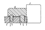
- the drawing shows a cross section through a flange 6 of a connector strip 1, and the associated cross section through a printed circuit board 2.
- the majority of the connector strip body is shown as a plan view to simplify the illustration.
- the one-piece contact elements consisting of contact springs and connection elements, which are held in chambers of the connector strip and make contact with the circuit board, are not shown in the drawing, since they are not essential to the invention.
- the task is to firmly connect the connector strip 1 to the printed circuit board 2.
- the connector strip 1 has a plurality of arbitrarily distributed flanges 6, which are provided with press-in pins 3.
- press-in pins are provided per flange.
- the press-in pin 3 immediately adjacent to the connector strip 1 is of larger dimensions. This press-in pin 3 has a larger diameter and. a greater length. A certain demonstration is thereby achieved.
- the press-in pin taking over the demonstration is dimensioned to be larger.
- the second press-in pin mainly serves to finally fix the connector strip with respect to the printed circuit board 2.
- the holes in the printed circuit board 2 required for receiving the press-in pin 3 are identified by reference number 5.
- crimp ribs 7 are provided on each strip pin directly adjacent to the strip body. These pinch ribs have a triangular cross section, which increases towards the underside of the flange 6. In addition to a firm contact of the printed circuit board 2 with the connector strip body, the pinch ribs 7 at the same time ensure that the plug-in force is also transmitted to the body of the connector strip 1 and is partly absorbed by it.
Claims (1)
- Barrette de connecteur électrique, équipée de plusieurs rangées d'éléments de contact qui sont reliés à l'aide d'éléments de raccordement, à une plaquette à circuits imprimés d'un module électrique, les sections des éléments de raccordement, qui ressortent des chambres de logement prévues pour les éléments de contact, étant recourbées en direction de la plaquette à circuits imprimés, et la barrette de connecteur (1) comportant, sur sa face arrière, plusieurs tétons enfichables à force, dirigés vers le bas, caractérisée par le fait qu'une nervure de serrage (7), qui possède une section transversale triangulaire dont la taille augmente en direction de la face inférieure de la bride (6), est formée sur le corps (1) de la barrette, en vis-à-vis de chaque téton enfichable à force (3), directement voisin du corps de la barrette.
Applications Claiming Priority (2)
| Application Number | Priority Date | Filing Date | Title |
|---|---|---|---|
| DE3441310 | 1984-11-12 | ||
| DE3441310 | 1984-11-12 |
Publications (3)
| Publication Number | Publication Date |
|---|---|
| EP0182070A2 EP0182070A2 (fr) | 1986-05-28 |
| EP0182070A3 EP0182070A3 (en) | 1988-09-14 |
| EP0182070B1 true EP0182070B1 (fr) | 1990-06-06 |
Family
ID=6250098
Family Applications (1)
| Application Number | Title | Priority Date | Filing Date |
|---|---|---|---|
| EP85112796A Expired - Lifetime EP0182070B1 (fr) | 1984-11-12 | 1985-10-09 | Bloc de connecteur électrique |
Country Status (4)
| Country | Link |
|---|---|
| US (1) | US4710132A (fr) |
| EP (1) | EP0182070B1 (fr) |
| JP (1) | JPS61121270A (fr) |
| DE (1) | DE3578104D1 (fr) |
Families Citing this family (13)
| Publication number | Priority date | Publication date | Assignee | Title |
|---|---|---|---|---|
| AT387126B (de) * | 1986-06-16 | 1988-12-12 | Alcatel Austria Ag | Halterung fuer leiterplatten |
| DE3824459A1 (de) * | 1988-07-19 | 1990-01-25 | Binder Franz Elektr | Einbaustecker, insbesondere fuer medizinische geraete |
| EP0397057B1 (fr) * | 1989-05-12 | 1994-07-27 | Siemens Aktiengesellschaft | Assemblage pour la connexion mécanique et électrique d'une plaque de câblage d'extension à une plaque de câblage de base |
| JP2791831B2 (ja) * | 1990-10-26 | 1998-08-27 | 日本エー・エム・ピー株式会社 | 電気コネクタ |
| DE4034789C1 (fr) * | 1990-11-02 | 1992-04-16 | C.A. Weidmueller Gmbh & Co, 4930 Detmold, De | |
| US5277618A (en) * | 1991-05-02 | 1994-01-11 | E. I. Du Pont Nemours And Company | Connector having fixing means for mounting on a substrate |
| NL192067C (nl) * | 1991-05-02 | 1997-01-07 | Du Pont Nederland | Connector met bevestigingsmiddelen voor montage op een substraat. |
| TW323002U (en) * | 1993-11-22 | 1997-12-11 | Molex Inc | Receptacle mounting means for IC card |
| CA2158703A1 (fr) * | 1994-09-30 | 1996-03-31 | Kevin G. Henderson | Connecteur electrique et dispositif pour aligner les broches de contact electrique |
| JP3148855B2 (ja) * | 1996-03-01 | 2001-03-26 | モレックス インコーポレーテッド | 電気コネクタ |
| JPH10228958A (ja) * | 1997-02-14 | 1998-08-25 | Yazaki Corp | コネクタ |
| JP4832109B2 (ja) * | 2006-02-27 | 2011-12-07 | 矢崎総業株式会社 | 電気接続箱 |
| EP3471520B1 (fr) | 2017-10-10 | 2021-10-06 | Vitesco Technologies GmbH | Agencement de montage de carte de circuit imprimé |
Family Cites Families (11)
| Publication number | Priority date | Publication date | Assignee | Title |
|---|---|---|---|---|
| US2976345A (en) * | 1957-10-31 | 1961-03-21 | Whitso Inc | Insulated electric terminal |
| US3000066A (en) * | 1959-06-29 | 1961-09-19 | United Carr Fastener Corp | Molding and the like fastening devices |
| US3319918A (en) * | 1965-06-18 | 1967-05-16 | Illinois Tool Works | Shock mounting groummet |
| DE1802821A1 (de) * | 1968-10-12 | 1970-06-04 | Standard Elek K Lorenz Ag | Hochpoliger Steckverbinder fuer die Fernsprech- oder eine andere Informationen verarbeitende Technik |
| US3727169A (en) * | 1970-11-12 | 1973-04-10 | Deutsch Co Electronic Co Divis | Connector for printed circuit boards |
| US4050769A (en) * | 1976-03-18 | 1977-09-27 | Elfab Corporation | Electrical connector |
| US4457570A (en) * | 1980-02-12 | 1984-07-03 | Virginia Patent Development Corporation | Connector for mating modular plug with printed circuit board |
| DE2925590A1 (de) * | 1978-06-29 | 1980-01-17 | Bunker Ramo | Elektrische kontaktanordnung fuer einen an einer gedruckten schaltung anschliessbaren verbinder |
| JPS5541682A (en) * | 1979-05-08 | 1980-03-24 | Sony Corp | Method of mounting terminals at printed board |
| DE2938760A1 (de) * | 1979-09-25 | 1981-04-02 | Siemens AG, 1000 Berlin und 8000 München | Kontaktfeder fuer eine niederohmige masseverbindung einer leiterplatte mit einem geerdeten baugruppentraeger |
| US4477142A (en) * | 1983-03-29 | 1984-10-16 | Amp Incorporated | Fastener |
-
1985
- 1985-10-02 US US06/783,112 patent/US4710132A/en not_active Expired - Lifetime
- 1985-10-09 EP EP85112796A patent/EP0182070B1/fr not_active Expired - Lifetime
- 1985-10-09 DE DE8585112796T patent/DE3578104D1/de not_active Expired - Lifetime
- 1985-11-12 JP JP60252136A patent/JPS61121270A/ja active Pending
Also Published As
| Publication number | Publication date |
|---|---|
| EP0182070A2 (fr) | 1986-05-28 |
| EP0182070A3 (en) | 1988-09-14 |
| JPS61121270A (ja) | 1986-06-09 |
| US4710132A (en) | 1987-12-01 |
| DE3578104D1 (de) | 1990-07-12 |
Similar Documents
| Publication | Publication Date | Title |
|---|---|---|
| DE69724036T2 (de) | Flachkabelverbindungs-Struktur | |
| DE69634005T2 (de) | Steckverbinder mit integriertem leiterplattenzusammenbau | |
| DE69814322T2 (de) | Verbinder für eine gedruckte Leiterplatte und Herstellungsverfahren dafür | |
| DE1765654A1 (de) | Anschlussvorrichtung fuer gedruckte Schaltungen | |
| EP0182070B1 (fr) | Bloc de connecteur électrique | |
| DE60309777T2 (de) | Anschlusskontakt für Leiterplatte | |
| DE2409075A1 (de) | Elektrischer verbinder | |
| DE69911911T2 (de) | Crimpanschlussklemme für flexible Leiterplatte und Crimpanordnung für Leitungsader | |
| DE2941029A1 (de) | Zum einpressverbinden mit einem elektrischen leiter vorgesehenen elektrischen anschlussteil, verfahren zum verbinden eines anschlussteils mit einem elektrischen leiter sowie verbinder mit einer mehrzahl elektrischer anschlussteile | |
| DE2234961C3 (de) | Verfahren zur Herstellung von Steckern für Schaltplatten | |
| DE4427451C1 (de) | Buchsenleiste oder 90 DEG -Stiftleiste | |
| DE102006011262A1 (de) | Elektrischer Verbinder und Verfahren zu dessen Herstellung | |
| DE202009014251U1 (de) | System zur Verbindung elektrischer Leiter mit voneinander verschiedenen Potentialen sowie Steckadapter für das System | |
| DE69923652T2 (de) | Modularer gefilterter Verbinder | |
| DE19607706A1 (de) | Koax-Verbinder | |
| EP0856911A1 (fr) | Bloc de connexion multipolaire | |
| DE4034789C1 (fr) | ||
| DE2007014A1 (de) | Elektrische Kontaktbuchse und Verfahren zu ihrer Herstellung | |
| DE3933658A1 (de) | Elektrischer steckverbinder | |
| EP1129511B1 (fr) | Composant electrique pour carte de circuits et procede pour implanter automatiquement des composants de ce type sur des cartes de circuits | |
| DE2303537A1 (de) | Anschlusschiene und verfahren zu ihrer herstellung | |
| DE60009024T2 (de) | Elektrischer Verbinder für ein Flachkabel | |
| DE8433087U1 (de) | Elektrische Steckverbinderleiste | |
| DE10157099B4 (de) | Elektrischer Verbinder für die Datentechnik | |
| EP1038335B1 (fr) | Ensemble de lames de contact destine a une barrette de connexion multiple pour des raccords de cables, et barrette de connexion multiple |
Legal Events
| Date | Code | Title | Description |
|---|---|---|---|
| PUAI | Public reference made under article 153(3) epc to a published international application that has entered the european phase |
Free format text: ORIGINAL CODE: 0009012 |
|
| AK | Designated contracting states |
Kind code of ref document: A2 Designated state(s): CH DE FR GB IT LI SE |
|
| PUAL | Search report despatched |
Free format text: ORIGINAL CODE: 0009013 |
|
| AK | Designated contracting states |
Kind code of ref document: A3 Designated state(s): CH DE FR GB IT LI SE |
|
| 17P | Request for examination filed |
Effective date: 19881010 |
|
| 17Q | First examination report despatched |
Effective date: 19890308 |
|
| GRAA | (expected) grant |
Free format text: ORIGINAL CODE: 0009210 |
|
| AK | Designated contracting states |
Kind code of ref document: B1 Designated state(s): CH DE FR GB IT LI SE |
|
| REF | Corresponds to: |
Ref document number: 3578104 Country of ref document: DE Date of ref document: 19900712 |
|
| ITF | It: translation for a ep patent filed |
Owner name: STUDIO JAUMANN |
|
| ET | Fr: translation filed | ||
| GBT | Gb: translation of ep patent filed (gb section 77(6)(a)/1977) | ||
| PLBE | No opposition filed within time limit |
Free format text: ORIGINAL CODE: 0009261 |
|
| STAA | Information on the status of an ep patent application or granted ep patent |
Free format text: STATUS: NO OPPOSITION FILED WITHIN TIME LIMIT |
|
| 26N | No opposition filed | ||
| ITTA | It: last paid annual fee | ||
| EAL | Se: european patent in force in sweden |
Ref document number: 85112796.9 |
|
| REG | Reference to a national code |
Ref country code: CH Ref legal event code: PUE Owner name: SIEMENS AKTIENGESELLSCHAFT BERLIN UND MUENCHEN -DA Ref country code: CH Ref legal event code: NV Representative=s name: RIEDERER HASLER & PARTNER PATENTANWAELTE AG |
|
| REG | Reference to a national code |
Ref country code: GB Ref legal event code: 732E |
|
| REG | Reference to a national code |
Ref country code: GB Ref legal event code: IF02 |
|
| PGFP | Annual fee paid to national office [announced via postgrant information from national office to epo] |
Ref country code: GB Payment date: 20040915 Year of fee payment: 20 |
|
| PGFP | Annual fee paid to national office [announced via postgrant information from national office to epo] |
Ref country code: FR Payment date: 20041004 Year of fee payment: 20 |
|
| PGFP | Annual fee paid to national office [announced via postgrant information from national office to epo] |
Ref country code: SE Payment date: 20041005 Year of fee payment: 20 |
|
| PGFP | Annual fee paid to national office [announced via postgrant information from national office to epo] |
Ref country code: DE Payment date: 20041029 Year of fee payment: 20 |
|
| PGFP | Annual fee paid to national office [announced via postgrant information from national office to epo] |
Ref country code: CH Payment date: 20050107 Year of fee payment: 20 |
|
| PG25 | Lapsed in a contracting state [announced via postgrant information from national office to epo] |
Ref country code: GB Free format text: LAPSE BECAUSE OF EXPIRATION OF PROTECTION Effective date: 20051008 |
|
| REG | Reference to a national code |
Ref country code: CH Ref legal event code: PL |
|
| REG | Reference to a national code |
Ref country code: GB Ref legal event code: PE20 |
|
| EUG | Se: european patent has lapsed |