EP0182070B1 - Electrical connector block - Google Patents
Electrical connector block Download PDFInfo
- Publication number
- EP0182070B1 EP0182070B1 EP85112796A EP85112796A EP0182070B1 EP 0182070 B1 EP0182070 B1 EP 0182070B1 EP 85112796 A EP85112796 A EP 85112796A EP 85112796 A EP85112796 A EP 85112796A EP 0182070 B1 EP0182070 B1 EP 0182070B1
- Authority
- EP
- European Patent Office
- Prior art keywords
- circuit board
- connector strip
- press
- strip
- printed circuit
- Prior art date
- Legal status (The legal status is an assumption and is not a legal conclusion. Google has not performed a legal analysis and makes no representation as to the accuracy of the status listed.)
- Expired - Lifetime
Links
Images
Classifications
-
- H—ELECTRICITY
- H01—ELECTRIC ELEMENTS
- H01R—ELECTRICALLY-CONDUCTIVE CONNECTIONS; STRUCTURAL ASSOCIATIONS OF A PLURALITY OF MUTUALLY-INSULATED ELECTRICAL CONNECTING ELEMENTS; COUPLING DEVICES; CURRENT COLLECTORS
- H01R12/00—Structural associations of a plurality of mutually-insulated electrical connecting elements, specially adapted for printed circuits, e.g. printed circuit boards [PCB], flat or ribbon cables, or like generally planar structures, e.g. terminal strips, terminal blocks; Coupling devices specially adapted for printed circuits, flat or ribbon cables, or like generally planar structures; Terminals specially adapted for contact with, or insertion into, printed circuits, flat or ribbon cables, or like generally planar structures
- H01R12/70—Coupling devices
- H01R12/7005—Guiding, mounting, polarizing or locking means; Extractors
- H01R12/7011—Locking or fixing a connector to a PCB
- H01R12/7064—Press fitting
Definitions
- the invention relates to an electrical connector strip which is provided with a plurality of rows of contact elements which are connected by means of connection elements to a printed circuit board of an electrical assembly, the portions of the connection elements projecting from the receiving chambers for the contact elements being bent toward the circuit board, and the connector strip being attached its rear has several flanges with downward facing press-in pins.
- Such a connector strip is known for example from DE-A 29 25 590.
- This known connector strip has at least two press-in pins which can be inserted into corresponding openings in the printed circuit.
- press-in pins When using several press-in pins, the use of which is desirable for reasons of strength, the problem arises that both the printed circuit board and the connector strip must be manufactured in such a way that a very high tolerance must be achieved because of the press-in pins. This leads to very expensive manufacturing processes.
- the object of the invention is to provide a connector strip of the type mentioned above, which does not necessarily have to meet the highest tolerance requirements for assembly with a printed circuit board.
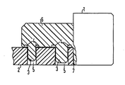
- the drawing shows a cross section through a flange 6 of a connector strip 1, and the associated cross section through a printed circuit board 2.
- the majority of the connector strip body is shown as a plan view to simplify the illustration.
- the one-piece contact elements consisting of contact springs and connection elements, which are held in chambers of the connector strip and make contact with the circuit board, are not shown in the drawing, since they are not essential to the invention.
- the task is to firmly connect the connector strip 1 to the printed circuit board 2.
- the connector strip 1 has a plurality of arbitrarily distributed flanges 6, which are provided with press-in pins 3.
- press-in pins are provided per flange.
- the press-in pin 3 immediately adjacent to the connector strip 1 is of larger dimensions. This press-in pin 3 has a larger diameter and. a greater length. A certain demonstration is thereby achieved.
- the press-in pin taking over the demonstration is dimensioned to be larger.
- the second press-in pin mainly serves to finally fix the connector strip with respect to the printed circuit board 2.
- the holes in the printed circuit board 2 required for receiving the press-in pin 3 are identified by reference number 5.
- crimp ribs 7 are provided on each strip pin directly adjacent to the strip body. These pinch ribs have a triangular cross section, which increases towards the underside of the flange 6. In addition to a firm contact of the printed circuit board 2 with the connector strip body, the pinch ribs 7 at the same time ensure that the plug-in force is also transmitted to the body of the connector strip 1 and is partly absorbed by it.
Description
Die Erfindung betrifft eine elektrische Steckverbinderleiste, die mit mehreren Reihen von Kontaktelementen versehen ist, die mittels Anschlußelementen mit einer Leiterplatte einer elektrischen Baugruppe verbunden sind, wobei die aus Aufnahmekammem für die Kontaktelemente herausragenden Abschnitte der Anschlußelemente zur Leiterplatte hin abgebogen sind, und wobei die Steckverbinderleiste an ihrer Rückseite mehrere Flansche mit nach unten gerichteten Einpreßzapfen aufweist.The invention relates to an electrical connector strip which is provided with a plurality of rows of contact elements which are connected by means of connection elements to a printed circuit board of an electrical assembly, the portions of the connection elements projecting from the receiving chambers for the contact elements being bent toward the circuit board, and the connector strip being attached its rear has several flanges with downward facing press-in pins.
Eine derartige Steckverbinderleiste ist zum Beispiel aus der DE-A 29 25 590 bekannt. Diese bekannte Steckverbinderleiste hat wenigstens zwei in entsprechende Öffnungen der gedruckten Schaltung einführbare Einpreßzapfen. Bei der Verwendung mehrerer Einpreßzapfen, deren Verwendung aus Festigkeitsgründen erwünscht ist, tritt das Problem auf, daß sowohl die Leiterplatte als auch die Steckverbinderleiste so gefertigt sein müssen, daß wegen der Einpreßzapfen eine sehr hohe Toleranz erreicht werden muß. Dies führt zu sehr teuren Herstellungsverfahren.Such a connector strip is known for example from DE-A 29 25 590. This known connector strip has at least two press-in pins which can be inserted into corresponding openings in the printed circuit. When using several press-in pins, the use of which is desirable for reasons of strength, the problem arises that both the printed circuit board and the connector strip must be manufactured in such a way that a very high tolerance must be achieved because of the press-in pins. This leads to very expensive manufacturing processes.
Aufgabe der Erfindung ist es, eine Steckverbinderleiste der obengenannten Art anzugeben, welche für den Zusammenbau mit einer Leiterplatte nicht unbedingt höchste Toleranzansprüche erfüllen muß.The object of the invention is to provide a connector strip of the type mentioned above, which does not necessarily have to meet the highest tolerance requirements for assembly with a printed circuit board.
Diese Aufgabe wird erfindungsgemäß für eine elektrische Steckverbinderleiste der eingangs genannten Art dadurch gelöst, daß gegenüber jedem dem Leistenkörper direkt benachbarten Einpreßzapfen am Leistenkörper eine einen dreieckigen Querschnitt aufweisende Quetschrippe, deren Querschnitt sich in Richtung zur Unterseite des Flansches vergrößert ist, gebildet ist.This object is achieved according to the invention for an electrical connector strip of the type mentioned at the outset in that a squeezing rib having a triangular cross section, the cross section of which is enlarged in the direction of the underside of the flange, is formed on each molding pin directly adjacent to the strip body.
Dadurch wird ein Toleranzausgleich zwischen dem eigentlichen Körper der Steckverbinderleiste und der Leiterplatte geschaffen. Gleichzeitig wird die Einpreßkraft dabei auch auf den Steckverbinderleistenkörper übertragen und von diesem mitaufgefangen.This creates a tolerance compensation between the actual body of the connector strip and the circuit board. At the same time, the press-in force is also transmitted to the connector body and is also absorbed by it.
Im folgenden wird die Erfindung anhand eines in der Zeichnung dargestellten Ausführungsbeispieles näher erläutert. Die Zeichnung zeigt einen Querschnitt durch einen Flansch 6 einer Steckverbinderleiste 1, sowie den dazugehörigen Querschnitt durch eine Leiterplatte 2. Dabei ist der größte Teil des Steckverbinderleistenkörpers zur Vereinfachung der Darstellung als Draufsicht dargestellt.The invention is explained in more detail below on the basis of an exemplary embodiment shown in the drawing. The drawing shows a cross section through a flange 6 of a connector strip 1, and the associated cross section through a printed circuit board 2. The majority of the connector strip body is shown as a plan view to simplify the illustration.
Die einstückigen Kontaktelemente bestehend aus Kontaktfedern und Anschlußelementen, die in Kammern der Steckverbinderleiste gehalten sind und den Kontakt zur Leiterplatte herstellen, sind in der Zeichnung nicht dargestellt, da sie nicht erfindungswesentlich sind. Wie eingangs erwähnt, besteht die Aufgabe darin, die Steckverbinderleiste 1 mit der Leiterplatte 2 fest zu verbinden. Dazu weist die Steckverbinderleiste 1 mehrere beliebig verteilte Flansche 6 auf, die mit Einpreßzapfen 3 versehen sind. Beim dargestellten Ausführungsbeispiel sind pro Flansch zwei Einpreßzapfen vorgesehen. Dabei ist, wie der Zeichnung zu entnehmen ist, der der Steckverbinderleiste 1 unmittelbar benachbarte Einpreßzapfen 3 stärker dimensioniert. Dieser Einpreßzapfen 3 weist einen größeren Durchmesser und. eine größere Länge auf. Dadurch wird eine gewisse Vorführung erreicht. Da während des Einpreßvorganges erhebliche Kräfte, besonders am Anfang auftreten können, ist der die Vorführung übernehmende Einpreßzapfen stärker dimensioniert. Der zweite Einpreßzapfen dient hauptsächlich einer endgültigen Fixierung der Steckverbinderleiste in bezug auf die Leiterplatte 2. Die zur Aufnahme der Einpreßzapfen 3 notwendigen Bohrungen in der Leiterplatte 2 sind mit dem Bezugszeichen 5 gekennzeichnet.The one-piece contact elements consisting of contact springs and connection elements, which are held in chambers of the connector strip and make contact with the circuit board, are not shown in the drawing, since they are not essential to the invention. As mentioned at the beginning, the task is to firmly connect the connector strip 1 to the printed circuit board 2. For this purpose, the connector strip 1 has a plurality of arbitrarily distributed flanges 6, which are provided with press-in pins 3. In the illustrated embodiment, two press-in pins are provided per flange. Here, as can be seen from the drawing, the press-in pin 3 immediately adjacent to the connector strip 1 is of larger dimensions. This press-in pin 3 has a larger diameter and. a greater length. A certain demonstration is thereby achieved. Since considerable forces, particularly at the beginning, can occur during the press-in process, the press-in pin taking over the demonstration is dimensioned to be larger. The second press-in pin mainly serves to finally fix the connector strip with respect to the printed circuit board 2. The holes in the printed circuit board 2 required for receiving the press-in pin 3 are identified by
Aufgrund der vorgegebenen Toleranzen zwischen dem Durchmesser der Einpreßzapfen und dem Durchmesser der Bohrungen 5 können durch einen Überschnitt beim Einpressen Späne entstehen. Diese würden sich zwischen Leiterplatte 2 und der Unterseite des Flansches 6 ablagern und ein planes Aufliegen des Flansches 6 auf der Leiterplatte 2 verhindern. Um dieses zu vermeiden, sind unterhalb der Einpreßzapfen an der Unterseite des Flansches 6 Hohlräume 4 vorgesehen. Diese dienen zur Aufnahme eventuell anfallender Späne. Diese Hohlräume sind zweckmäßigerweise so ausgebildet, daß sie Späne, die über den gesamten Umfang des Einpreßzapfens auftreten, aufnehmen können. Die einfachste Art wäre es, diese Hohlräume als kreisförmige Nuten auszubilden, wobei der Innendurchmesser dieser Nuten dem Durchmesser der Einpreßzapfen 3 entspricht. Die äußere Begrenzung der Hohlräume 4 muß aber durchaus nicht kreisförmig gestaltet sein.Due to the specified tolerances between the diameter of the press-in pins and the diameter of the
Um ein festes Anliegen der Leiterplatte 2 an den eigentlichen Körper der Steckverbinderleiste trotz bestehender Toleranzen zu ermöglichen, sind gegenüber jedem dem Leistenkörper direkt benachbarten Einpreßzapfen am Leistenkörper Quetschrippen 7 vorgesehen. Diese Quetschrippen weisen einen dreieckigen Querschnitt auf, der sich zur Unterseite des Flansches 6 hin vergrößert. Neben einem festen Anliegen der Leiterplatte 2 an den Steckverbinderleistenkörper wird gleichzeitig durch die Quetschrippen 7 erreicht, daß die Steckkraft auch auf den Körper der Steckverbinderleiste 1 übertragen wird und von diesem zu einem Teil mit aufgefangen wird.In order to allow the printed circuit board 2 to lie firmly against the actual body of the connector strip despite existing tolerances,
Claims (1)
- Electrical plug connector strip, which is provided with a plurality of rows of contact elements that are connected by means of terminal elements to a printed circuit board of an electrical assembly, the sections of the terminal elements projecting from receptacle chambers for the contact elements being bent toward the circuit board, and the back side of the plug connector strip (1) having a plurality of flanges (6) having downwardly directed insertion posts, characterized in that a pinch rib (7) having a triangular cross-section that enlarges in the direction towards the underside of the flange (6) is fashioned on the strip body (1) opposite every insertion post (3) directly adjacent to the strip body.
Applications Claiming Priority (2)
| Application Number | Priority Date | Filing Date | Title |
|---|---|---|---|
| DE3441310 | 1984-11-12 | ||
| DE3441310 | 1984-11-12 |
Publications (3)
| Publication Number | Publication Date |
|---|---|
| EP0182070A2 EP0182070A2 (en) | 1986-05-28 |
| EP0182070A3 EP0182070A3 (en) | 1988-09-14 |
| EP0182070B1 true EP0182070B1 (en) | 1990-06-06 |
Family
ID=6250098
Family Applications (1)
| Application Number | Title | Priority Date | Filing Date |
|---|---|---|---|
| EP85112796A Expired - Lifetime EP0182070B1 (en) | 1984-11-12 | 1985-10-09 | Electrical connector block |
Country Status (4)
| Country | Link |
|---|---|
| US (1) | US4710132A (en) |
| EP (1) | EP0182070B1 (en) |
| JP (1) | JPS61121270A (en) |
| DE (1) | DE3578104D1 (en) |
Families Citing this family (13)
| Publication number | Priority date | Publication date | Assignee | Title |
|---|---|---|---|---|
| AT387126B (en) * | 1986-06-16 | 1988-12-12 | Alcatel Austria Ag | BRACKET FOR PCB |
| DE3824459A1 (en) * | 1988-07-19 | 1990-01-25 | Binder Franz Elektr | Installation plug, especially for medical appliances |
| DE59006551D1 (en) * | 1989-05-12 | 1994-09-01 | Siemens Ag | Arrangement for the mechanical and electrical connection of a supplementary circuit board to a basic circuit board. |
| JP2791831B2 (en) * | 1990-10-26 | 1998-08-27 | 日本エー・エム・ピー株式会社 | Electrical connector |
| DE4034789C1 (en) * | 1990-11-02 | 1992-04-16 | C.A. Weidmueller Gmbh & Co, 4930 Detmold, De | |
| NL192067C (en) * | 1991-05-02 | 1997-01-07 | Du Pont Nederland | Connector with fasteners for mounting on a substrate. |
| US5277618A (en) * | 1991-05-02 | 1994-01-11 | E. I. Du Pont Nemours And Company | Connector having fixing means for mounting on a substrate |
| TW323002U (en) * | 1993-11-22 | 1997-12-11 | Molex Inc | Receptacle mounting means for IC card |
| CA2158703A1 (en) * | 1994-09-30 | 1996-03-31 | Kevin G. Henderson | Electrical connector and alignment apparatus for contact pins thereof |
| JP3148855B2 (en) * | 1996-03-01 | 2001-03-26 | モレックス インコーポレーテッド | Electrical connector |
| JPH10228958A (en) * | 1997-02-14 | 1998-08-25 | Yazaki Corp | Connector |
| JP4832109B2 (en) * | 2006-02-27 | 2011-12-07 | 矢崎総業株式会社 | Electrical junction box |
| EP3471520B1 (en) | 2017-10-10 | 2021-10-06 | Vitesco Technologies GmbH | Printed circuit board mounting arrangement |
Family Cites Families (11)
| Publication number | Priority date | Publication date | Assignee | Title |
|---|---|---|---|---|
| US2976345A (en) * | 1957-10-31 | 1961-03-21 | Whitso Inc | Insulated electric terminal |
| US3000066A (en) * | 1959-06-29 | 1961-09-19 | United Carr Fastener Corp | Molding and the like fastening devices |
| US3319918A (en) * | 1965-06-18 | 1967-05-16 | Illinois Tool Works | Shock mounting groummet |
| DE1802821A1 (en) * | 1968-10-12 | 1970-06-04 | Standard Elek K Lorenz Ag | Multi-pole connector for telephone or other information processing technology |
| US3727169A (en) * | 1970-11-12 | 1973-04-10 | Deutsch Co Electronic Co Divis | Connector for printed circuit boards |
| US4050769A (en) * | 1976-03-18 | 1977-09-27 | Elfab Corporation | Electrical connector |
| US4457570A (en) * | 1980-02-12 | 1984-07-03 | Virginia Patent Development Corporation | Connector for mating modular plug with printed circuit board |
| DE2925590A1 (en) * | 1978-06-29 | 1980-01-17 | Bunker Ramo | ELECTRICAL CONTACT ARRANGEMENT FOR A CONNECTOR CONNECTABLE TO A PRINTED CIRCUIT |
| JPS5541682A (en) * | 1979-05-08 | 1980-03-24 | Sony Corp | Method of mounting terminals at printed board |
| DE2938760A1 (en) * | 1979-09-25 | 1981-04-02 | Siemens AG, 1000 Berlin und 8000 München | CONTACT SPRING FOR A LOW-OHMED GROUND CONNECTION OF A PCB WITH A GROUNDED SUBCARD |
| US4477142A (en) * | 1983-03-29 | 1984-10-16 | Amp Incorporated | Fastener |
-
1985
- 1985-10-02 US US06/783,112 patent/US4710132A/en not_active Expired - Lifetime
- 1985-10-09 EP EP85112796A patent/EP0182070B1/en not_active Expired - Lifetime
- 1985-10-09 DE DE8585112796T patent/DE3578104D1/en not_active Expired - Lifetime
- 1985-11-12 JP JP60252136A patent/JPS61121270A/en active Pending
Also Published As
| Publication number | Publication date |
|---|---|
| EP0182070A3 (en) | 1988-09-14 |
| JPS61121270A (en) | 1986-06-09 |
| US4710132A (en) | 1987-12-01 |
| EP0182070A2 (en) | 1986-05-28 |
| DE3578104D1 (en) | 1990-07-12 |
Similar Documents
| Publication | Publication Date | Title |
|---|---|---|
| DE69724036T2 (en) | Flat cable connection structure | |
| DE69634005T2 (en) | CONNECTORS WITH INTEGRATED PCB ASSEMBLY | |
| EP0677898B1 (en) | Connector for backplanes | |
| DE69814322T2 (en) | Printed circuit board connector and manufacturing method therefor | |
| DE1765654A1 (en) | Connection device for printed circuits | |
| EP0182070B1 (en) | Electrical connector block | |
| DE60309777T2 (en) | Connection contact for printed circuit board | |
| DE2409075A1 (en) | ELECTRIC CONNECTOR | |
| DE69911911T2 (en) | Crimp connection terminal for flexible circuit board and crimp arrangement for cable core | |
| DE2941029A1 (en) | ELECTRICAL CONNECTING PART PROVIDED FOR PRESS-IN CONNECTING, METHOD FOR CONNECTING A CONNECTING PART TO AN ELECTRICAL LADDER AND CONNECTOR WITH A MULTIPLE RANGE OF ELECTRICAL CONNECTING PARTS | |
| DE2234961C3 (en) | Process for the production of connectors for circuit boards | |
| DE4427451C1 (en) | Socket strip or 90 DEG pin strip | |
| DE102006011262A1 (en) | Electrical connector and method of making the same | |
| DE202009014251U1 (en) | System for connecting electrical conductors with mutually different potentials as well as plug-in adapters for the system | |
| DE69923652T2 (en) | Modular filtered connector | |
| DE19607706A1 (en) | Coax connector | |
| EP0856911A1 (en) | Multipole terminal block | |
| DE4034789C1 (en) | ||
| DE2007014A1 (en) | Electrical contact socket and process for their manufacture | |
| DE3933658A1 (en) | ELECTRICAL CONNECTOR | |
| EP1129511B1 (en) | Electric components for printed boards and method for automatically inserting said components in printed boards | |
| DE2303537A1 (en) | CONNECTING RAIL AND METHOD OF MANUFACTURING IT | |
| DE60009024T2 (en) | Electrical connector for a flat cable | |
| DE8433087U1 (en) | Electrical connector strip | |
| DE10157099B4 (en) | Electrical connector for data technology |
Legal Events
| Date | Code | Title | Description |
|---|---|---|---|
| PUAI | Public reference made under article 153(3) epc to a published international application that has entered the european phase |
Free format text: ORIGINAL CODE: 0009012 |
|
| AK | Designated contracting states |
Kind code of ref document: A2 Designated state(s): CH DE FR GB IT LI SE |
|
| PUAL | Search report despatched |
Free format text: ORIGINAL CODE: 0009013 |
|
| AK | Designated contracting states |
Kind code of ref document: A3 Designated state(s): CH DE FR GB IT LI SE |
|
| 17P | Request for examination filed |
Effective date: 19881010 |
|
| 17Q | First examination report despatched |
Effective date: 19890308 |
|
| GRAA | (expected) grant |
Free format text: ORIGINAL CODE: 0009210 |
|
| AK | Designated contracting states |
Kind code of ref document: B1 Designated state(s): CH DE FR GB IT LI SE |
|
| REF | Corresponds to: |
Ref document number: 3578104 Country of ref document: DE Date of ref document: 19900712 |
|
| ITF | It: translation for a ep patent filed |
Owner name: STUDIO JAUMANN |
|
| ET | Fr: translation filed | ||
| GBT | Gb: translation of ep patent filed (gb section 77(6)(a)/1977) | ||
| PLBE | No opposition filed within time limit |
Free format text: ORIGINAL CODE: 0009261 |
|
| STAA | Information on the status of an ep patent application or granted ep patent |
Free format text: STATUS: NO OPPOSITION FILED WITHIN TIME LIMIT |
|
| 26N | No opposition filed | ||
| ITTA | It: last paid annual fee | ||
| EAL | Se: european patent in force in sweden |
Ref document number: 85112796.9 |
|
| REG | Reference to a national code |
Ref country code: CH Ref legal event code: PUE Owner name: SIEMENS AKTIENGESELLSCHAFT BERLIN UND MUENCHEN -DA Ref country code: CH Ref legal event code: NV Representative=s name: RIEDERER HASLER & PARTNER PATENTANWAELTE AG |
|
| REG | Reference to a national code |
Ref country code: GB Ref legal event code: 732E |
|
| REG | Reference to a national code |
Ref country code: GB Ref legal event code: IF02 |
|
| PGFP | Annual fee paid to national office [announced via postgrant information from national office to epo] |
Ref country code: GB Payment date: 20040915 Year of fee payment: 20 |
|
| PGFP | Annual fee paid to national office [announced via postgrant information from national office to epo] |
Ref country code: FR Payment date: 20041004 Year of fee payment: 20 |
|
| PGFP | Annual fee paid to national office [announced via postgrant information from national office to epo] |
Ref country code: SE Payment date: 20041005 Year of fee payment: 20 |
|
| PGFP | Annual fee paid to national office [announced via postgrant information from national office to epo] |
Ref country code: DE Payment date: 20041029 Year of fee payment: 20 |
|
| PGFP | Annual fee paid to national office [announced via postgrant information from national office to epo] |
Ref country code: CH Payment date: 20050107 Year of fee payment: 20 |
|
| PG25 | Lapsed in a contracting state [announced via postgrant information from national office to epo] |
Ref country code: GB Free format text: LAPSE BECAUSE OF EXPIRATION OF PROTECTION Effective date: 20051008 |
|
| REG | Reference to a national code |
Ref country code: CH Ref legal event code: PL |
|
| REG | Reference to a national code |
Ref country code: GB Ref legal event code: PE20 |
|
| EUG | Se: european patent has lapsed |