EP1129511B1 - Electric components for printed boards and method for automatically inserting said components in printed boards - Google Patents
Electric components for printed boards and method for automatically inserting said components in printed boards Download PDFInfo
- Publication number
- EP1129511B1 EP1129511B1 EP99960853A EP99960853A EP1129511B1 EP 1129511 B1 EP1129511 B1 EP 1129511B1 EP 99960853 A EP99960853 A EP 99960853A EP 99960853 A EP99960853 A EP 99960853A EP 1129511 B1 EP1129511 B1 EP 1129511B1
- Authority
- EP
- European Patent Office
- Prior art keywords
- circuit board
- printed circuit
- housing
- stud
- pins
- Prior art date
- Legal status (The legal status is an assumption and is not a legal conclusion. Google has not performed a legal analysis and makes no representation as to the accuracy of the status listed.)
- Expired - Lifetime
Links
Images

Classifications
-
- H—ELECTRICITY
- H01—ELECTRIC ELEMENTS
- H01R—ELECTRICALLY-CONDUCTIVE CONNECTIONS; STRUCTURAL ASSOCIATIONS OF A PLURALITY OF MUTUALLY-INSULATED ELECTRICAL CONNECTING ELEMENTS; COUPLING DEVICES; CURRENT COLLECTORS
- H01R24/00—Two-part coupling devices, or either of their cooperating parts, characterised by their overall structure
- H01R24/38—Two-part coupling devices, or either of their cooperating parts, characterised by their overall structure having concentrically or coaxially arranged contacts
- H01R24/40—Two-part coupling devices, or either of their cooperating parts, characterised by their overall structure having concentrically or coaxially arranged contacts specially adapted for high frequency
- H01R24/50—Two-part coupling devices, or either of their cooperating parts, characterised by their overall structure having concentrically or coaxially arranged contacts specially adapted for high frequency mounted on a PCB [Printed Circuit Board]
-
- H—ELECTRICITY
- H01—ELECTRIC ELEMENTS
- H01R—ELECTRICALLY-CONDUCTIVE CONNECTIONS; STRUCTURAL ASSOCIATIONS OF A PLURALITY OF MUTUALLY-INSULATED ELECTRICAL CONNECTING ELEMENTS; COUPLING DEVICES; CURRENT COLLECTORS
- H01R12/00—Structural associations of a plurality of mutually-insulated electrical connecting elements, specially adapted for printed circuits, e.g. printed circuit boards [PCB], flat or ribbon cables, or like generally planar structures, e.g. terminal strips, terminal blocks; Coupling devices specially adapted for printed circuits, flat or ribbon cables, or like generally planar structures; Terminals specially adapted for contact with, or insertion into, printed circuits, flat or ribbon cables, or like generally planar structures
- H01R12/70—Coupling devices
- H01R12/7005—Guiding, mounting, polarizing or locking means; Extractors
- H01R12/7011—Locking or fixing a connector to a PCB
- H01R12/707—Soldering or welding
-
- H—ELECTRICITY
- H01—ELECTRIC ELEMENTS
- H01R—ELECTRICALLY-CONDUCTIVE CONNECTIONS; STRUCTURAL ASSOCIATIONS OF A PLURALITY OF MUTUALLY-INSULATED ELECTRICAL CONNECTING ELEMENTS; COUPLING DEVICES; CURRENT COLLECTORS
- H01R9/00—Structural associations of a plurality of mutually-insulated electrical connecting elements, e.g. terminal strips or terminal blocks; Terminals or binding posts mounted upon a base or in a case; Bases therefor
- H01R9/03—Connectors arranged to contact a plurality of the conductors of a multiconductor cable, e.g. tapping connections
- H01R9/05—Connectors arranged to contact a plurality of the conductors of a multiconductor cable, e.g. tapping connections for coaxial cables
- H01R9/0515—Connection to a rigid planar substrate, e.g. printed circuit board
-
- H—ELECTRICITY
- H05—ELECTRIC TECHNIQUES NOT OTHERWISE PROVIDED FOR
- H05K—PRINTED CIRCUITS; CASINGS OR CONSTRUCTIONAL DETAILS OF ELECTRIC APPARATUS; MANUFACTURE OF ASSEMBLAGES OF ELECTRICAL COMPONENTS
- H05K3/00—Apparatus or processes for manufacturing printed circuits
- H05K3/30—Assembling printed circuits with electric components, e.g. with resistor
- H05K3/32—Assembling printed circuits with electric components, e.g. with resistor electrically connecting electric components or wires to printed circuits
- H05K3/34—Assembling printed circuits with electric components, e.g. with resistor electrically connecting electric components or wires to printed circuits by soldering
- H05K3/3447—Lead-in-hole components
-
- H—ELECTRICITY
- H01—ELECTRIC ELEMENTS
- H01R—ELECTRICALLY-CONDUCTIVE CONNECTIONS; STRUCTURAL ASSOCIATIONS OF A PLURALITY OF MUTUALLY-INSULATED ELECTRICAL CONNECTING ELEMENTS; COUPLING DEVICES; CURRENT COLLECTORS
- H01R2103/00—Two poles
-
- H—ELECTRICITY
- H01—ELECTRIC ELEMENTS
- H01R—ELECTRICALLY-CONDUCTIVE CONNECTIONS; STRUCTURAL ASSOCIATIONS OF A PLURALITY OF MUTUALLY-INSULATED ELECTRICAL CONNECTING ELEMENTS; COUPLING DEVICES; CURRENT COLLECTORS
- H01R24/00—Two-part coupling devices, or either of their cooperating parts, characterised by their overall structure
- H01R24/38—Two-part coupling devices, or either of their cooperating parts, characterised by their overall structure having concentrically or coaxially arranged contacts
-
- H—ELECTRICITY
- H05—ELECTRIC TECHNIQUES NOT OTHERWISE PROVIDED FOR
- H05K—PRINTED CIRCUITS; CASINGS OR CONSTRUCTIONAL DETAILS OF ELECTRIC APPARATUS; MANUFACTURE OF ASSEMBLAGES OF ELECTRICAL COMPONENTS
- H05K2201/00—Indexing scheme relating to printed circuits covered by H05K1/00
- H05K2201/09—Shape and layout
- H05K2201/09009—Substrate related
- H05K2201/09045—Locally raised area or protrusion of insulating substrate
-
- H—ELECTRICITY
- H05—ELECTRIC TECHNIQUES NOT OTHERWISE PROVIDED FOR
- H05K—PRINTED CIRCUITS; CASINGS OR CONSTRUCTIONAL DETAILS OF ELECTRIC APPARATUS; MANUFACTURE OF ASSEMBLAGES OF ELECTRICAL COMPONENTS
- H05K2201/00—Indexing scheme relating to printed circuits covered by H05K1/00
- H05K2201/09—Shape and layout
- H05K2201/09818—Shape or layout details not covered by a single group of H05K2201/09009 - H05K2201/09809
- H05K2201/09827—Tapered, e.g. tapered hole, via or groove
-
- H—ELECTRICITY
- H05—ELECTRIC TECHNIQUES NOT OTHERWISE PROVIDED FOR
- H05K—PRINTED CIRCUITS; CASINGS OR CONSTRUCTIONAL DETAILS OF ELECTRIC APPARATUS; MANUFACTURE OF ASSEMBLAGES OF ELECTRICAL COMPONENTS
- H05K2201/00—Indexing scheme relating to printed circuits covered by H05K1/00
- H05K2201/10—Details of components or other objects attached to or integrated in a printed circuit board
- H05K2201/10007—Types of components
- H05K2201/10189—Non-printed connector
-
- H—ELECTRICITY
- H05—ELECTRIC TECHNIQUES NOT OTHERWISE PROVIDED FOR
- H05K—PRINTED CIRCUITS; CASINGS OR CONSTRUCTIONAL DETAILS OF ELECTRIC APPARATUS; MANUFACTURE OF ASSEMBLAGES OF ELECTRICAL COMPONENTS
- H05K2201/00—Indexing scheme relating to printed circuits covered by H05K1/00
- H05K2201/10—Details of components or other objects attached to or integrated in a printed circuit board
- H05K2201/10431—Details of mounted components
- H05K2201/10568—Integral adaptations of a component or an auxiliary PCB for mounting, e.g. integral spacer element
-
- H—ELECTRICITY
- H05—ELECTRIC TECHNIQUES NOT OTHERWISE PROVIDED FOR
- H05K—PRINTED CIRCUITS; CASINGS OR CONSTRUCTIONAL DETAILS OF ELECTRIC APPARATUS; MANUFACTURE OF ASSEMBLAGES OF ELECTRICAL COMPONENTS
- H05K2201/00—Indexing scheme relating to printed circuits covered by H05K1/00
- H05K2201/10—Details of components or other objects attached to or integrated in a printed circuit board
- H05K2201/10431—Details of mounted components
- H05K2201/10598—Means for fastening a component, a casing or a heat sink whereby a pressure is exerted on the component towards the PCB
-
- H—ELECTRICITY
- H05—ELECTRIC TECHNIQUES NOT OTHERWISE PROVIDED FOR
- H05K—PRINTED CIRCUITS; CASINGS OR CONSTRUCTIONAL DETAILS OF ELECTRIC APPARATUS; MANUFACTURE OF ASSEMBLAGES OF ELECTRICAL COMPONENTS
- H05K3/00—Apparatus or processes for manufacturing printed circuits
- H05K3/30—Assembling printed circuits with electric components, e.g. with resistor
- H05K3/32—Assembling printed circuits with electric components, e.g. with resistor electrically connecting electric components or wires to printed circuits
- H05K3/34—Assembling printed circuits with electric components, e.g. with resistor electrically connecting electric components or wires to printed circuits by soldering
- H05K3/3457—Solder materials or compositions; Methods of application thereof
- H05K3/3485—Applying solder paste, slurry or powder
Definitions
- the invention relates to an electrical circuit board component, in particular RF coaxial connector part, at the housing of the component through the solder joints between the provided on its underside SMD solder terminals and this PCB side associated solder terminals is attached to the circuit board.
- Electric circuit board components in particular HF coaxial connector parts, find at electrical transmission and Connecting devices a numerous use. Basically, there are three different types of connection for the electrical connection between the associated ones component-side and board-side connections to Application.
- the connectors are made of solder pins made of thin wires are. From such solder pins can also be in relatively large Number of components of small dimensions use be made.
- such connector parts need be placed on the printed circuit board by hand during assembly, as the threading of the thin solder pins in their assigned PCB-side connection holes is difficult. After placing such connector parts on the circuit board soldering the solder pins in their assigned board side through holes Wave soldering.
- connection - third connection - as for example in which by the document DE 197 16 139 C1 known connector part is used are for the electrical connections between component and circuit board of surface solder joints, so-called SMD (Surface Mounted Device) solder connections, use made.
- SMD Surface Mounted Device solder connections
- the Assembly of printed circuit boards with SMD solder connections Components has in contrast to those with press pins or solder pins the big advantage that they are simple and easy fast with "pick & place” machines. Of the Disadvantage is the low strength of these solder joints induced anchoring of the component on the PCB. For this reason, the component must here in addition fastened by screws or rivets to the circuit board be to prevent the SMD solder joints through sometimes unavoidable stronger mechanical loads damaged or even torn off.
- the invention is based on the object for the sufficient Fixing of electrical connections provided with SMD solder terminals Specify components on printed circuit boards another solution, which works without screws or rivets and manufacturing technology is particularly easy.
- the invention is based on the finding that the Bestükkung of printed circuit boards with the help of "pick & place” machines is also possible if the component soldering pin-like Has connecting elements, the circuit board side in soldered to these associated continuous contacted holes become. Condition here is only that their cross section Enough is that they are from "pick & place” cars when placing the component on the circuit board too can be used as centering.
- Fig. 1 The illustrated in Fig. 1 first embodiment of a electrical circuit board component is a HF-angle connector part. It corresponds in its basic structure to the Connector part, by the already in the introduction Reference DE 197 16 139 C1 is known. Out For this reason it should suffice, if here on the structure the design of this first embodiment only insofar is considered to be for the understanding of the invention is required and otherwise for more details Reference is made to the cited reference.
- the housing 1 which may also be a metal housing exists here from metallized plastic. It points to the mating connector side 2 four coaxial sockets 3 in a row-column arrangement on.
- the layer thickness of the metallization of the housing 1 is at least equal to the penetration depth of via the printed circuit board component to be transmitted electromagnetic Waves.
- the housing 1 has contact feet 4 and 5, of which the Contact feet 4 in a variety on the outside of the Housing 1 are arranged near its bottom 6.
- the Contact feet 4 have footprints that are as tin-plated SMD solder connections are performed.
- the contact feet 5 are also SMD solder terminals and consist of at the Bottom 6 exiting, parallel thereto bent ends the metallic inner conductor.
- the contact feet 4 and 5 serve the electrical connection of their SMD solder terminals associated with them solder terminals on the in Fig. 1 only schematically indicated in broken lines PCB 7th
- the contact feet 4 are on the outside of the side walls 8 and 9 and the rear wall 10 of the housing 1 in larger numbers provided and each have a comb-like structure on. They have a support web-like shape and protrude with their SMD connections slightly above the bottom 6 of the Housing 1 addition. The same applies to the contact feet 5 of the inner conductor ends. Other contact feet 4 are on the edge of the bottom 6 on the side of the mating connector side 2 provided.
- the arrangement of the contact feet 4 and 5 on the outside the side walls 8 and 9 and the rear wall 10 and the edge side at the bottom 6 on the side of the mating connector 2 is for soldering their SMD solder connections on the PCB 7 important because the circulating heat used in the soldering process be brought so well to the SMD Lötanschadore can. In addition, it can easily be checked in hindsight, whether the solder joints are perfect. To connect the case 1 with the PCB 7 for all SMD solder connections to ensure proper solder joints, it is appropriate between all SMD connections of the contact feet 4 and 5 provide a planarity tolerance ⁇ 0.1 mm.
- the number of total provided contact feet 4, whose SMD solder terminals with the metallization of the housing. 1 are electrically connected, is chosen as large as possible, after the manufacture of the SMD solder joints a the best possible attachment of the housing 1 on the circuit board 7 to ensure.
- the number of total provided contact feet 4, whose SMD solder terminals with the metallization of the housing. 1 are electrically connected, is chosen as large as possible, after the manufacture of the SMD solder joints a the best possible attachment of the housing 1 on the circuit board 7 to ensure.
- a larger number of SMD solder joints are low, so that to be challenged for such attachment mechanical Resilience not sufficiently ensured can be.
- FIG. 1 shows between the Contact feet 4 both on the outsides of the side walls 8 and 9 and the rear wall 10 and at the edge of the bottom 2 on the side of the mating connector 2 more solderable Bolt pins 11 provided over the contact feet. 4 and 5 protrude and when placed on the circuit board. 7 in their associated contacted bolt holes 12 in the circuit board 7 intervene in which they are soldered.
- the Bolt pins 11 are made as the housing 1 made of plastic. They are like the contact feet 4 support-like to the Housing walls molded and metallized.
- soldering of the housing-side pin pins 11 in the circuit board side contacted bolt holes 12 can as when soldering solder pins made by wave soldering be, in which the circuit board 7 with the on its top 13 patch housing 1 with its bottom 14 via a Löt-Schwallbad is performed. In this case, so must the assembly of the printed circuit board 7 with a housing 1 two Soldering operations are performed.
- a first soldering operation is required for the manufacture the electrical connections between the housing side SMD solder terminals of contact feet 4 and 5 and the these on the circuit board 7 associated solder terminals.
- the circuit board 7 passes through the patch Housing 1 an SMD soldering oven.
- has a second soldering operation with a soldering wave for soldering the housing-side pin pins 11 in their assigned board-side contacted bolt holes 12 performed become.
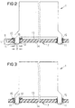
- bolt holes 12 can also in extraordinary advantageously also after the SMD soldering be carried out so that when the assembly of the circuit board 7 with a housing 1 only a soldering operation must be performed. This fact should be discussed below will be discussed in more detail with reference to FIGS. 2 and 3.
- FIGs. 2 and 3 show a schematic representation of the process of the SMD soldering process.
- Each of Figs. 2 and 3 shows a On the circuit board 7 mounted housing 1.
- Each of the housing 1 is shown exclusively with two pin pins 11, one of which on the left side wall 8 and he another is formed on the right side wall 9. Both pin pins 11 engage in their associated bolt holes 12 in the circuit board 7 a.
- solder connections on the top 13 of the circuit board 7 be provided with a solder paste pad.
- a solder paste mask is used.
- the solder paste 15 is applied over it. After passing through the SMD soldering oven, the solder paste is as the respective right half of Figs. 2 and 3 well lets into the cavity between the pin pin 11 and the contacted wall of the bolt hole 12 is flowed, thereby the stud pin 11 is firmly soldered in the bolt hole.
Abstract
Description
Die Erfindung bezieht sich auf ein elektrisches Leiterplatten-Bauteil, insbesondere HF-Koaxial-Steckverbinderteil, bei dem das Gehäuse des Bauteils durch die Lötverbindungen zwischen den an seiner Unterseite vorgesehenen SMD-Lötanschlüssen und diesen leiterplatten-seitig zugeordneten Lötanschlüssen auf der Leiterplatte befestigt ist.The invention relates to an electrical circuit board component, in particular RF coaxial connector part, at the housing of the component through the solder joints between the provided on its underside SMD solder terminals and this PCB side associated solder terminals is attached to the circuit board.
Elektrische Leiterplatten-Bauteile, insbesondere HF-Koaxial-Steckverbinderteile, finden bei elektrischen Übertragungsund Verbindungseinrichtungen eine zahlreiche Verwendung. Grundsätzlich kommen drei verschiedene Anschlußarten für die elektrische Verbindung zwischen den einander zugeordneten bauteileseitigen und leiterplattenseitigen Anschlüssen zur Anwendung.Electric circuit board components, in particular HF coaxial connector parts, find at electrical transmission and Connecting devices a numerous use. Basically, there are three different types of connection for the electrical connection between the associated ones component-side and board-side connections to Application.
Bei der Anschlußart - erste Anschlußart -, wie sie beispielsweise bei dem durch die Literaturstelle EP 0 582 960 A1 bekannten Steckverbinderteil zur Anwendung kommt, wird von Preßstiften Gebrauch gemacht, durch die sich ein Lötvorgang erübrigt. Die Verwendung solcher relativ voluminösen Preßstifte setzt jedoch voraus, daß ihre Anzahl mit Rücksicht auf die möglichst kleinen Abmessungen solcher Bauteile pro Bauteil begrenzt ist. Erheblich begrenzt ist ihre Anzahl pro Bauteil aber auch dadurch, daß der aufzuwendende Preßdruck beim Einpressen der bauteileseitigen Preßstifte in die ihnen zugeordneten leiterplattenseitigen kontaktierten Anschlußlöcher einen durch die Festigkeit des Bauteils bedingten Wert nicht überschreiten darf. Der aufzuwendende Preßdruck ist nämlich der Anzahl der vorgesehenen Preßstifte proportional. Für eine automatische Bestückung von Leiterplatten mit solchen Bauteilen sind sehr kostenaufwendige Vorrichtungen erforderlich. When the Anschlussart - first connection -, as for example in which by the document EP 0 582 960 A1 known Connector part is used, is of Preßstiften made use of by a soldering process unnecessary. The use of such relatively bulky press pins assumes, however, that their number takes into account the smallest possible dimensions of such components per component is limited. Considerably limited is their number per Component but also in that the expended pressing pressure when pressing the component-side press pins in them associated printed circuit board-side contacted terminal holes a value due to the strength of the component must not exceed. The expended pressing pressure is namely, the number of provided press pins proportional. For automatic assembly of printed circuit boards with such Components require very expensive devices.
Bei der Anschlußart - zweite Anschlußart -, wie sie beispielsweise bei dem durch die Literaturstelle EP 0 488 482 A1 bekannten Steckverbinderteil zur Anwendung kommt, bestehen die Anschlüsse aus Lötstiften, die aus dünnen Drähten hergestellt sind. Von solchen Lötstiften kann auch in relativ großer Anzahl bei recht klein dimensionierten Bauteilen Gebrauch gemacht werden. Allerdings müssen solche Steckverbinderteile bei der Montage von Hand auf die Leiterplatte aufgesetzt werden, da das Einfädeln der dünnen Lötstifte in die ihnen zugeordneten leiterplattenseitigen Anschlußlöcher schwierig ist. Nach dem Aufsetzen solcher Steckverbinderteile auf die Leiterplatte erfolgt das Verlöten der Lötstifte in den ihnen zugeordneten leiterplattenseitgen Anschlußlöchern durch Schwalllöten.In the Anschlussart - second connection -, as for example in the case of the document EP 0 488 482 A1 known connector part is used, exist the connectors are made of solder pins made of thin wires are. From such solder pins can also be in relatively large Number of components of small dimensions use be made. However, such connector parts need be placed on the printed circuit board by hand during assembly, as the threading of the thin solder pins in their assigned PCB-side connection holes is difficult. After placing such connector parts on the circuit board soldering the solder pins in their assigned board side through holes Wave soldering.
Bei der Anschlußart - dritte Anschlußart -, wie sie beispielsweise bei dem durch die Literaturstelle DE 197 16 139 C1 bekannten Steckverbinderteil zur Anwendung kommt, werden für die elektrischen Verbindungen zwischen Bauteil und Leiterplatte von Oberflächen-Lötanschlüssen, sogenannte SMD (Surface Mounted Device)-Lötanschlüsse, Gebrauch gemacht. Die Bestückung der Leiterplatten mit SMD-Lötanschlüsse aufweisenden Bauteilen hat im Gegensatz zu solchen mit Preßstiften oder Lötstiften den großen Vorteil, daß sie sich einfach und schnell mit "Pick&Place"-Automaten durchführen läßt. Der Nachteil ist die geringe Festigkeit der durch diese Lötverbindungen herbeigeführten Verankerung des Bauteils auf der Leiterplatte. Aus diesem Grunde muß hier das Bauteil zusätzlich durch Schrauben oder Nieten an der Leiterplatte befestigt werden, um zu verhindern, daß die SMD-Lötverbindungen durch mitunter unvermeidbare stärkere mechanischen Belastungen beschädigt werden oder sogar abreißen.When the connection - third connection -, as for example in which by the document DE 197 16 139 C1 known connector part is used are for the electrical connections between component and circuit board of surface solder joints, so-called SMD (Surface Mounted Device) solder connections, use made. The Assembly of printed circuit boards with SMD solder connections Components has in contrast to those with press pins or solder pins the big advantage that they are simple and easy fast with "pick & place" machines. Of the Disadvantage is the low strength of these solder joints induced anchoring of the component on the PCB. For this reason, the component must here in addition fastened by screws or rivets to the circuit board be to prevent the SMD solder joints through sometimes unavoidable stronger mechanical loads damaged or even torn off.
Der Erfindung liegt die Aufgabe zugrunde, für die ausreichende Befestigung von mit SMD-Lötanschlüssen versehenen elektrischen Bauteilen auf Leiterplatten eine weitere Lösung anzugeben, die ohne Schrauben oder Nieten auskommt und fertigungstechnisch besonders einfach ist.The invention is based on the object for the sufficient Fixing of electrical connections provided with SMD solder terminals Specify components on printed circuit boards another solution, which works without screws or rivets and manufacturing technology is particularly easy.
Diese Aufgabe wird gemäß der Erfindung für eine solches elektrischen Leiterplatten-Bauteil dadurch gelöst, daß das Gehäuse für seine zusätzliche Befestigung auf der Leiterplatte an seiner Unterseite mehrere lötbare Bolzenstifte aufweist, die in ihnen auf der Leiterplatte zugeordnete durchgehende kontaktierte Bolzenlöcher eingreifen und hierin verlötet sind.This object is achieved according to the invention for such an electrical Printed circuit board component solved by the fact that the housing for its additional attachment to the circuit board its underside has a plurality of solderable stud pins, the in their on the printed circuit board associated continuous contacted Engage bolt holes and soldered therein.
Der Erfindung liegt die Erkenntnis zugrunde, daß die Bestükkung von Leiterplatten unter Zuhilfenahme von "Pick&Place"-Automaten auch dann möglich ist, wenn das Bauteil lötstiftartige Verbindungselemente aufweist, die leiterplattenseitig in diesen zugeordneten durchgehenden kontaktierten Löchern verlötet werden. Voraussetzung hierbei ist nur, daß ihr Querschnitt ausreichend groß ist, daß sie von "Pick&Place"-Autoaten beim Aufsetzen des Bauteils auf die Leiterplatte auch als Zentriermittel verwendet werden können.The invention is based on the finding that the Bestükkung of printed circuit boards with the help of "pick & place" machines is also possible if the component soldering pin-like Has connecting elements, the circuit board side in soldered to these associated continuous contacted holes become. Condition here is only that their cross section Enough is that they are from "pick & place" cars when placing the component on the circuit board too can be used as centering.
Zweckmäßige Ausgestaltungen des Gegenstandes nach Patentanspruch 1 sind in den weiteren Patentansprüchen 2 bis 8 angegeben.Advantageous embodiments of the article according to claim 1 are given in the further claims 2 to 8.
In Weiterbildung der Erfindung ist in dem Patentanspruch 9 noch ein besonders zeit- und kostengünstiges Verfahren für die automatische Bestückung von Leiterplatten mit von der Erfindung Gebrauch machenden Leiterplatten-Bauteilen angegeben.In development of the invention is in the claim yet a particularly time-consuming and cost-effective method for the automatic assembly of printed circuit boards with from the Invention making use of printed circuit board components.
Anhand eines Ausführungsbeispiels, das in der Zeichnung dargestellt ist, soll die Erfindung im folgenden noch näher beschrieben werden. In der Zeichnung bedeuten
- Fig. 1
- die perspektivische Darstellung eines Ausführungsbeispiels in Form eines HF-Winkel-Steckverbinderteils,
- Fig. 2
- die schematische Darstellung der Verankerung gehäuseseitiger Bolzenstifte in leiterplattenseitigen Bolzenlöchern in einer ersten Ausführungsform,
- Fig. 3
- die schematische Darstellung der Verankerung gehäuseseitiger Bolzenstifte in leiterplattenseitigen Bolzenlöchern in einer zweiten Ausführungsform.
- Fig. 1
- the perspective view of an embodiment in the form of an HF-angle connector part,
- Fig. 2
- the schematic representation of the anchoring of housing-side pin pins in the circuit board side bolt holes in a first embodiment,
- Fig. 3
- the schematic representation of the anchoring housing side bolt pins in the circuit board side bolt holes in a second embodiment.
Das in Fig. 1 dargestellte erste Ausführungsbeispiel eines elektrischen Leiterplatten-Bauteils ist ein HF-Winkelsteckverbinderteil. Es entspricht in seiner Grundstruktur dem Steckverbinderteil, das durch die bereits in der Einleitung angegebene Literaturstelle DE 197 16 139 C1 bekannt ist. Aus diesem Grunde dürfte es genügen, wenn hier auf die Struktur der Bauform dieses ersten Ausführungsbeispieles nur insoweit eingegangen wird, als es für das Verständnis der Erfindung erforderlich ist und im übrigen hinsichtlich näherer Details auf die genannte Literaturstelle verwiesen wird.The illustrated in Fig. 1 first embodiment of a electrical circuit board component is a HF-angle connector part. It corresponds in its basic structure to the Connector part, by the already in the introduction Reference DE 197 16 139 C1 is known. Out For this reason it should suffice, if here on the structure the design of this first embodiment only insofar is considered to be for the understanding of the invention is required and otherwise for more details Reference is made to the cited reference.
Das Gehäuse 1, das auch ein Metallgehäuse sein kann, besteht
hier aus metallisiertem Kunststoff. Es weist auf der Gegensteckerseite
2 vier Koaxialbuchsen 3 in einer Reihen-Spaltenanordnung
auf. Die Schichtstärke der Metallisierung des Gehäuses
1 ist dabei wenigstens gleich der Eindringtiefe der
über das Leiterplatten-Bauteil zu übertragenden elektromagnetischen
Wellen.The housing 1, which may also be a metal housing exists
here from metallized plastic. It points to the mating connector side
2 four
Das Gehäuse 1 hat Kontakt-Standfüße 4 und 5, von denen die
Kontakt-Standfüße 4 in einer Vielzahl an der Außenseite des
Gehäuses 1 in Nähe seiner Unterseite 6 angeordnet sind. Die
Kontakt-Standfüße 4 haben Standflächen, die als verzinnbare
SMD-Lötanschlüsse ausgeführt sind. Die Kontakt-Standfüße 5
sind ebenfalls SMD-Lötanschlüsse und bestehen aus den an der
Unterseite 6 austretenden, parallel hierzu abgebogenen Enden
der metallischen Innenleiter. Die Kontakt-Standfüße 4 und 5
dienen der elektrischen Verbindung ihrer SMD-Lötanschlüsse
mit ihnen zugeordneten Lötanschlüssen auf der in Fig. 1 lediglich
schematisch in unterbrochenen Linien angegebenen Leiterplatte
7.The housing 1 has
Die Kontakt-Standfüße 4 sind an-der Außenseite der Seitenwände
8 und 9 und der Rückwand 10 des Gehäuses 1 in größerer Anzahl
vorgesehen und weisen jeweils eine kammartige Struktur
auf. Sie haben eine stützstegartige Formgebung und ragen mit
ihren SMD-Anschlüssen geringfügig über die Unterseite 6 des
Gehäuses 1 hinaus. Entsprechendes gilt für die Kontakt-Standfüße
5 der Innenleiterenden. Weitere Kontakt-Standfüße 4
sind am Rand der Unterseite 6 auf seiten der Gegensteckerseite
2 vorgesehen.The
Die Anordnung der Kontakt-Standfüße 4 und 5 an der Außenseite
der Seitenwände 8 und 9 und der Rückwand 10 sowie randseitig
an der Unterseite 6 auf seiten der Gegensteckerseite 2 ist
für das Anlöten ihrer SMD-Lötanschlüsse auf der Leiterplatte
7 von Bedeutung, weil die beim Lötvorgang eingesetzte Umluftwärme
so gut an die SMD-Lötanschüsse herangeführt werden
kann. Außerdem kann so im Nachhinein leicht überprüft werden,
ob die Lötstellen einwandfrei sind. Um beim Verbinden des Gehäuses
1 mit der Leiterplatte 7 für alle SMD-Lötanschlüsse
einwandfreie Lötverbindungen sicherzustellen, ist es angebracht,
zwischen allen SMD-Anschlüssen der Kontakt-Standfüße
4 und 5 eine Planitätstoleranz < 0,1 mm vorzusehen.The arrangement of the
Die Anzahl der insgesamt vorgesehenen Kontakt-Standfüße 4,
deren SMD-Lötanschlüsse mit der Metallisierung des Gehäuses 1
elektrisch leitend verbunden sind, wird möglichst groß gewählt,
um nach der Herstellung der SMD-Lötverbindungen eine
möglichst gute Befestigung des Gehäuses 1 auf der Leiterplatte
7 sicherzustellen. Wie die Praxis zeigt, ist die durch
SMD-Lötverbindungen erreichbare Gehäusebefestigung auch bei
einer größeren Anzahl von SMD-Lötverbindungen jedoch gering,
so daß die für eine solche Befestigung zu fordernde mechanische
Belastbarkeit nicht in ausreichendem Maße sichergestellt
werden kann.The number of total provided
Für eine'ausreichende mechanische Befestigung des Gehäuses 1
auf der Leiterplatte 7 sind, wie Fig. 1 zeigt zwischen den
Kontakt-Standfüßen 4 sowohl an den Außenseiten der Seitenwände
8 und 9 und der Rückwand 10 als auch am Rand der Unterseite
2 auf seiten der Gegensteckerseite 2 mehrere lötfähige
Bolzenstifte 11 vorgesehen, die über die Kontakt-Standfüße 4
und 5 hinausragen und beim Aufsetzten auf die Leiterplatte 7
in ihnen zugeordnete kontaktierte Bolzenlöcher 12 in der Leiterplatte
7 eingreifen, in denen sie verlötet werden. Die
Bolzenstifte 11 bestehen wie das Gehäuse 1 aus Kunststoff.
Sie sind wie die Kontakt-Standfüße 4 stützstegartig an die
Gehäusewandungen angeformt und metallisiert.For a sufficient mechanical fastening of the housing 1
on the circuit board 7, as FIG. 1 shows between the
Das Verlöten der gehäuseseitigen Bolzenstifte 11 in den leiterplattenseitigen
kontaktierten Bolzenlöcher 12 kann wie
beim Verlöten von Lötstiften durch Schwallöten vorgenommen
werden, bei dem die Leiterplatte 7 mit dem auf ihre Oberseite
13 aufgesetzten Gehäuse 1 mit ihrer Unterseite 14 über ein
Löt-Schwallbad geführt wird. In diesem Falle müssen also bei
der Bestückung der Leiterplatte 7 mit einem Gehäuse 1 zwei
Löt-Arbeitsvorgänge durchgeführt werden.The soldering of the housing-
Ein erster Löt-Arbeitsvorgang ist erforderlich für die Herstellung
der elektrischen Verbindungen zwischen den gehäuseseitigen
SMD-Lötanschlüssen der Kontakt-Standfüße 4 und 5 und
den diesen auf der Leiterplatte 7 zugeordneten Lötanschlüssen.
Hierbei durchläuft die Leiterplatte 7 mit dem aufgesetzten
Gehäuse 1 einen SMD-Lötofen. Sodann muß ein zweiter Löt-Arbeitsvorgang
mit einem Löt-Schwallbad für das Verlöten der
gehäuseseitigen Bolzenstifte 11 in den ihnen zugeordneten
leiterplattenseitigen kontaktierten Bolzenlöchern 12 durchgeführt
werden. Das Verlöten der gehäuseseitigen Bolzenstifte
11 in den ihnen zugeordneten leiterplattenseitigen kontaktierten
Bolzenlöchern 12 kann aber auch in außerordentlich
vorteilhafter Weise ebenfalls nach dem SMD-Lötverfahren
durchgeführt werden, so daß bei der Bestückung der Leiterplatte
7 mit einem Gehäuse 1 lediglich ein Löt-Arbeitsvorgang
durchgeführt werden muß. Auf diesen Sachverhalt soll im folgenden
noch anhand der Fig. 2 und 3 näher eingegangen werden.A first soldering operation is required for the manufacture
the electrical connections between the housing side
SMD solder terminals of
Die Fig. 2 und 3 zeigen in schematischer Darstellung den Ablauf
des SMD-Lötverfahrens. Jede der Fig. 2 und 3 zeigt ein
auf die Leiterplatte 7 aufgesetztes Gehäuse 1. Jedes der Gehäuse
1 ist ausschließlich mit zwei Bolzenstiften 11 dargestellt,
von denen der eine an der linken Seitenwand 8 und er
andere an der rechten Seitenwand 9 angeformt ist. Beide Bolzenstifte
11 greifen in die ihnen zugeordneten Bolzenlöcher
12 in der Leiterplatte 7 ein. Durch die mittige senkrechte
Unterteilung des Gehäuses 1 und der Leiterplatte 7 in eine
linke und eine rechte Hälfte soll der SMD-Lötvorgang angedeutet
werden. Hierbei ist jeweils das leiterplattenseitige kontaktierte
Bolzenloch 12 mit dem hierin eingreifenden gehäuseseitigen
Bolzenstift 11 bei der linken Hälfte im Zustand vor
und bei der rechten Hälfte im Zustand nach dem Durchgang der
Leiterplatte 7 mit dem aufgesetzten Gehäuse 1 durch den SMD-Lötofen
dargestellt.Figs. 2 and 3 show a schematic representation of the process
of the SMD soldering process. Each of Figs. 2 and 3 shows a
On the circuit board 7 mounted housing 1. Each of the housing
1 is shown exclusively with two pin pins 11,
one of which on the left side wall 8 and he
another is formed on the
Bevor das Gehäuse 1 auf die Leiterplatte 7 aufgesetzt wird,
müssen alle Lötanschlüsse auf der Oberseite 13 der Leiterplatte
7 mit einer Lötpastenauflage versehen werden. Hierzu
wird eine Lötpastenmaske verwendet. Im Bereich der Bolzenlöcher
12 wird die Lötpaste 15 über diese hinweg aufgetragen.
Nach dem Durchlauf durch den SMD-Lötofen ist die Lötpaste,
wie die jeweils rechte Hälfte der Fig. 2 und 3 gut erkennen
läßt, in den Hohlraum zwischen dem Bolzenstift 11 und der
kontaktierten Wandung des Bolzenlochs 12 eingeflossen, wodurch
der Bolzenstift 11 im Bolzenloch fest verlötet wird.Before the housing 1 is placed on the circuit board 7,
All solder connections on the top 13 of the circuit board
7 be provided with a solder paste pad. For this
a solder paste mask is used. In the area of bolt holes
12, the
Der Unterschied zwischen den Fig. 2 und 3 besteht lediglich
in der Form der Bolzenlöcher 12. Während die kontaktierte Innenwandung
16 der Bolzenlöcher 12 in Fig. 2 senkrecht ausgeführt
ist, ist die kontaktierte Innenwandung 17 der Bolzenlöcher
12 in Fig. 3 leicht konusförmig gestaltet. Diese Ausführungsform
kann mitunter sinnvoll sein, um zu verhindern, daß
beim Durchgang der Leiterplatte 7 durch den SMD-Lötofen die
verflüssigte Lötpaste 15 teilweise nach unten von der Unterseite
14 der Leiterplatte 7 abtropft. Im allgemeinen läßt
sich dies jedoch bei senkrecht gestalteter Innenwandung 16
durch eine geeignete, aufeinander abgestimmte Bemessung von
Bolzenstift- und Bolzenloch-Durchmesser selbst dann unterbinden,
wenn sich die Bolzenstifte 11 zu ihrem freien Ende hin
leicht konisch verjüngen. Beim in der Zeichnung dargestellten
Ausführungsbeispiel wurden bei einer Dicke S der Leiterplatte
7 von 1,6 mm folgende Abmessungen vorgesehen:
Claims (9)
- An electrical printed circuit board component, in particular an HF coaxial plug connector part, in which the housing (1) of the component is secured to the printed circuit board (7) by the soldered connections between the SMD soldered terminals provided on its underside (6) and soldered terminals associated with these on the printed circuit board side, characterised in that
for the purpose of additionally securing it to the printed circuit board (7), the housing (1) has on its underside (6) a plurality of solderable stud-like pins (11) which engage in contact-making stud holes (12) associated therewith in the printed circuit board (7), passing all the way through, and which are soldered therein. - An electrical printed circuit board component according to Claim 1, characterised in that the soldered connections between the stud-like pins (11) on the housing side in the stud holes (12) on the printed circuit board side are made in the form of SMD soldered connections.
- An electrical printed circuit board component according to Claim 1 or 2, characterised in that
the housing (1), including its stud-like pins (11), is made from synthetic material, and
at least the stud-like pins (11) are provided with a solderable metallisation. - An electrical printed circuit board component according to Claim 3, characterised in that the metallised stud-like pins (11) are at reference potential.
- An electrical printed circuit board component according to one of the preceding claims, characterised in that the cross-section of the stud-like pins (11) is selected to be larger than the cross-section of the solder pins which are conventionally used in components of this type and which are made from thin wires.
- An electrical printed circuit board component according to Claim 5, characterised in that the cross-section of the stud-like pins (11) is selected, taking into account their number and the nature of their material, to be large enough for the mechanical loading capacity of the securing of the housing (1) to the printed circuit board (7) to adequately fulfil the requirements made thereof.
- An electrical printed circuit board component according to one of the preceding claims, characterised in that the stud-like pins (11) projecting beyond the underside (6) of the housing (1) form extension pieces which are preferably integrally formed on the lower edge of the housing (1) on the outsides of its side walls (8, 9) and its rear wall (10).
- An electrical printed circuit board component according to one of the preceding claims, characterised in that
the contact-making inner wall (17) of the stud holes (12) in the printed circuit board side is shaped to be slightly conical, and
the stud holes (12) shaped in this way in this case have their larger internal diameter on that side of the printed circuit board (7) on which the stud-like pins (11) on the housing side engage in the stud holes (12). - A process for automatically fitting electrical printed circuit board components according to Claim 1 onto printed circuit boards, characterised in that
in a first step, with the aid of a solder paste mask, all the soldering terminals and all the stud holes (12) on the printed circuit board (7) are provided with a layer of solder paste (15),
in a second step the housing (1) is picked up by a pick & place machine and, exploiting the possibility for centring which is provided by the stud-like pins (11) on the housing side and the stud holes (12) on the printed circuit board side, is placed on the printed circuit board (7) and
in a third step the printed circuit board (7) runs, together with the housing (1) placed thereon, through an SMD soldering furnace in which, in one operational procedure, the SMD soldering terminals of the contact feet (4, 5) on the housing side are firmly soldered to the soldering terminals associated therewith on the printed circuit board side on the one hand, and on the other hand the stud-like pins (11) on the housing side are firmly soldered in the stud holes (12) associated therewith on the printed circuit board side.
Applications Claiming Priority (3)
| Application Number | Priority Date | Filing Date | Title |
|---|---|---|---|
| DE19851868 | 1998-11-10 | ||
| DE19851868A DE19851868C1 (en) | 1998-11-10 | 1998-11-10 | Electrical circuit board component and method for the automatic assembly of circuit boards with such components |
| PCT/DE1999/003493 WO2000028627A1 (en) | 1998-11-10 | 1999-11-02 | Electric components for printed boards and method for automatically inserting said components in printed boards |
Publications (2)
| Publication Number | Publication Date |
|---|---|
| EP1129511A1 EP1129511A1 (en) | 2001-09-05 |
| EP1129511B1 true EP1129511B1 (en) | 2003-03-19 |
Family
ID=7887337
Family Applications (1)
| Application Number | Title | Priority Date | Filing Date |
|---|---|---|---|
| EP99960853A Expired - Lifetime EP1129511B1 (en) | 1998-11-10 | 1999-11-02 | Electric components for printed boards and method for automatically inserting said components in printed boards |
Country Status (7)
| Country | Link |
|---|---|
| US (1) | US6793501B1 (en) |
| EP (1) | EP1129511B1 (en) |
| AT (1) | ATE235113T1 (en) |
| DE (2) | DE19851868C1 (en) |
| ES (1) | ES2194537T3 (en) |
| NO (1) | NO317123B1 (en) |
| WO (1) | WO2000028627A1 (en) |
Families Citing this family (8)
| Publication number | Priority date | Publication date | Assignee | Title |
|---|---|---|---|---|
| GB2371261B (en) * | 2001-01-22 | 2004-04-07 | Itt Mfg Enterprises Inc | Electrical component with conductive tracks |
| US6716039B1 (en) * | 2002-10-17 | 2004-04-06 | Molex Incorporated | Board mounted electrical connector |
| JP2004206924A (en) * | 2002-12-24 | 2004-07-22 | Auto Network Gijutsu Kenkyusho:Kk | Mounting structure of connector, mounting method thereof |
| US6948977B1 (en) * | 2004-08-05 | 2005-09-27 | Bob Behrent | Connector assembly and assembly method |
| DE202005020107U1 (en) * | 2005-12-23 | 2007-02-15 | Kathrein-Werke Kg | On a printed circuit board electrically connected coaxial H-connector device and associated connector unit |
| DE202006000720U1 (en) * | 2006-01-17 | 2006-04-20 | Receptec Gmbh | HF plug-fastening means |
| JP2018181696A (en) * | 2017-04-18 | 2018-11-15 | 株式会社フジクラ | Coaxial connector |
| BE1029962B1 (en) * | 2021-11-26 | 2023-06-26 | Phoenix Contact Gmbh & Co | Solderable insulator for fixing to a printed circuit board |
Family Cites Families (13)
| Publication number | Priority date | Publication date | Assignee | Title |
|---|---|---|---|---|
| GB8515831D0 (en) * | 1985-06-21 | 1985-07-24 | Harwin Engineers Sa | Socket assembly |
| US4826442A (en) | 1986-12-19 | 1989-05-02 | Amp Incorporated | Solderable connector retention feature |
| GB8726188D0 (en) | 1987-11-09 | 1987-12-16 | Amp Great Britain | Securing insulating housing of electrical connector |
| DE3738545A1 (en) * | 1987-11-13 | 1989-05-24 | Harting Elektronik Gmbh | Device for mounting plug connectors on printed circuit boards |
| GB8908411D0 (en) * | 1989-04-13 | 1989-06-01 | Amp Holland | Surface mount electrical connector |
| US5169343A (en) | 1990-11-29 | 1992-12-08 | E. I. Du Pont De Nemours And Company | Coax connector module |
| US5141445A (en) | 1991-04-30 | 1992-08-25 | Thomas & Betts Corporation | Surface mounted electrical connector |
| DE9210810U1 (en) * | 1992-08-12 | 1992-10-15 | Siemens Ag, 8000 Muenchen, De | |
| US5616035A (en) * | 1993-03-31 | 1997-04-01 | Berg Technology, Inc. | Electrical connector |
| US5394609A (en) * | 1993-10-26 | 1995-03-07 | International Business Machines, Corporation | Method and apparatus for manufacture of printed circuit cards |
| DE4337408A1 (en) * | 1993-11-02 | 1995-05-04 | Siemens Ag | Coaxial high-frequency connector with circuit board connection |
| GB2303258A (en) * | 1995-07-07 | 1997-02-12 | Harting Elektronik Gmbh | Shielded electrical connector |
| DE19716139C1 (en) * | 1997-04-17 | 1998-06-18 | Siemens Ag | Multiple high frequency coaxial plug connector unit |
-
1998
- 1998-11-10 DE DE19851868A patent/DE19851868C1/en not_active Expired - Fee Related
-
1999
- 1999-11-02 EP EP99960853A patent/EP1129511B1/en not_active Expired - Lifetime
- 1999-11-02 DE DE59904665T patent/DE59904665D1/en not_active Expired - Lifetime
- 1999-11-02 US US09/831,415 patent/US6793501B1/en not_active Expired - Lifetime
- 1999-11-02 ES ES99960853T patent/ES2194537T3/en not_active Expired - Lifetime
- 1999-11-02 AT AT99960853T patent/ATE235113T1/en not_active IP Right Cessation
- 1999-11-02 WO PCT/DE1999/003493 patent/WO2000028627A1/en active IP Right Grant
- 1999-11-03 NO NO19995380A patent/NO317123B1/en unknown
Also Published As
| Publication number | Publication date |
|---|---|
| NO995380L (en) | 2000-05-11 |
| DE59904665D1 (en) | 2003-04-24 |
| ATE235113T1 (en) | 2003-04-15 |
| ES2194537T3 (en) | 2003-11-16 |
| DE19851868C1 (en) | 2001-10-31 |
| EP1129511A1 (en) | 2001-09-05 |
| US6793501B1 (en) | 2004-09-21 |
| NO995380D0 (en) | 1999-11-03 |
| NO317123B1 (en) | 2004-08-16 |
| WO2000028627A1 (en) | 2000-05-18 |
Similar Documents
| Publication | Publication Date | Title |
|---|---|---|
| DE3544838C2 (en) | ||
| DE60026949T2 (en) | Interconnects | |
| DE19753839C1 (en) | For coaxial angle plug-type connection unit | |
| DE2525166A1 (en) | CONTACT PROBE DEVICE | |
| DE102009058825A1 (en) | Contact device for fastening to a printed circuit board, method for attaching a contact device to a printed circuit board and printed circuit board | |
| DE19809138A1 (en) | Printed circuit board with SMD components | |
| EP0906008A2 (en) | Plastic housing for an electric board | |
| EP1129511B1 (en) | Electric components for printed boards and method for automatically inserting said components in printed boards | |
| DE10061613A1 (en) | Electric pluggable device with holder for an electronic component e.g. for automobiles, has frame with end section having a fixture element extending from end section, and a guide channel is provided in housing for receiving fixture element | |
| EP0182070B1 (en) | Electrical connector block | |
| DE19607706A1 (en) | Coax connector | |
| DE10029025A1 (en) | Integrated circuit socket e.g. for ball grid array device, has upper contact pins which are displaceable and mechanically biased to extend beyond upper surface of base | |
| DE10158384A1 (en) | plug | |
| EP1175712B1 (en) | Printed circuit board connector | |
| DE3501711C2 (en) | ||
| EP0918374B1 (en) | High Frequency coaxial connector | |
| DE60037717T2 (en) | DATA CARRIER WITH INTEGRATED CIRCUIT AND TRANSMISSION COIL | |
| DE202009017984U1 (en) | press-fit | |
| EP3740050A1 (en) | Printed circuit board with a connector | |
| EP1022810B1 (en) | Method for connecting a cable with a printed circuit board and housing with cable connected to the circuit board according to the method | |
| DE60201537T2 (en) | ELECTRICAL CONNECTION ARRANGEMENT FOR ELECTRONIC COMPONENTS | |
| DE102004049575A1 (en) | Electrical terminal for connecting conductor cable to PCB, has terminal unit provided for pressing in conductor cable for electrical link of conductor cable, where terminal unit is designed as spike | |
| DE60003942T2 (en) | ELECTRICAL CONNECTOR AND MANUFACTURING METHOD THEREFOR | |
| DE102016120180B4 (en) | PCB and multiple terminal | |
| DE1640005A1 (en) | Procedure for connecting module assemblies |
Legal Events
| Date | Code | Title | Description |
|---|---|---|---|
| PUAI | Public reference made under article 153(3) epc to a published international application that has entered the european phase |
Free format text: ORIGINAL CODE: 0009012 |
|
| 17P | Request for examination filed |
Effective date: 20010403 |
|
| AK | Designated contracting states |
Kind code of ref document: A1 Designated state(s): AT BE CH CY DE DK ES FI FR GB GR IE IT LI LU MC NL PT SE |
|
| GRAG | Despatch of communication of intention to grant |
Free format text: ORIGINAL CODE: EPIDOS AGRA |
|
| 17Q | First examination report despatched |
Effective date: 20020116 |
|
| GRAG | Despatch of communication of intention to grant |
Free format text: ORIGINAL CODE: EPIDOS AGRA |
|
| GRAH | Despatch of communication of intention to grant a patent |
Free format text: ORIGINAL CODE: EPIDOS IGRA |
|
| GRAH | Despatch of communication of intention to grant a patent |
Free format text: ORIGINAL CODE: EPIDOS IGRA |
|
| GRAA | (expected) grant |
Free format text: ORIGINAL CODE: 0009210 |
|
| AK | Designated contracting states |
Designated state(s): AT BE CH CY DE DK ES FI FR GB GR IE IT LI LU MC NL PT SE |
|
| PG25 | Lapsed in a contracting state [announced via postgrant information from national office to epo] |
Ref country code: GR Free format text: LAPSE BECAUSE OF FAILURE TO SUBMIT A TRANSLATION OF THE DESCRIPTION OR TO PAY THE FEE WITHIN THE PRESCRIBED TIME-LIMIT Effective date: 20030319 |
|
| REG | Reference to a national code |
Ref country code: GB Ref legal event code: FG4D Free format text: NOT ENGLISH |
|
| REG | Reference to a national code |
Ref country code: CH Ref legal event code: EP |
|
| REG | Reference to a national code |
Ref country code: SE Ref legal event code: TRGR Ref country code: CH Ref legal event code: NV Representative=s name: RITSCHER & PARTNER AG PATENTANWAELTE |
|
| REG | Reference to a national code |
Ref country code: IE Ref legal event code: FG4D Free format text: GERMAN |
|
| REF | Corresponds to: |
Ref document number: 59904665 Country of ref document: DE Date of ref document: 20030424 Kind code of ref document: P |
|
| GBT | Gb: translation of ep patent filed (gb section 77(6)(a)/1977) |
Effective date: 20030512 |
|
| PG25 | Lapsed in a contracting state [announced via postgrant information from national office to epo] |
Ref country code: DK Free format text: LAPSE BECAUSE OF FAILURE TO SUBMIT A TRANSLATION OF THE DESCRIPTION OR TO PAY THE FEE WITHIN THE PRESCRIBED TIME-LIMIT Effective date: 20030619 |
|
| PG25 | Lapsed in a contracting state [announced via postgrant information from national office to epo] |
Ref country code: PT Free format text: LAPSE BECAUSE OF FAILURE TO SUBMIT A TRANSLATION OF THE DESCRIPTION OR TO PAY THE FEE WITHIN THE PRESCRIBED TIME-LIMIT Effective date: 20030620 |
|
| ET | Fr: translation filed | ||
| PG25 | Lapsed in a contracting state [announced via postgrant information from national office to epo] |
Ref country code: LU Free format text: LAPSE BECAUSE OF NON-PAYMENT OF DUE FEES Effective date: 20031102 Ref country code: CY Free format text: LAPSE BECAUSE OF FAILURE TO SUBMIT A TRANSLATION OF THE DESCRIPTION OR TO PAY THE FEE WITHIN THE PRESCRIBED TIME-LIMIT Effective date: 20031102 Ref country code: AT Free format text: LAPSE BECAUSE OF NON-PAYMENT OF DUE FEES Effective date: 20031102 |
|
| REG | Reference to a national code |
Ref country code: ES Ref legal event code: FG2A Ref document number: 2194537 Country of ref document: ES Kind code of ref document: T3 |
|
| PG25 | Lapsed in a contracting state [announced via postgrant information from national office to epo] |
Ref country code: MC Free format text: LAPSE BECAUSE OF NON-PAYMENT OF DUE FEES Effective date: 20031130 |
|
| PLBE | No opposition filed within time limit |
Free format text: ORIGINAL CODE: 0009261 |
|
| STAA | Information on the status of an ep patent application or granted ep patent |
Free format text: STATUS: NO OPPOSITION FILED WITHIN TIME LIMIT |
|
| 26N | No opposition filed |
Effective date: 20031222 |
|
| PGFP | Annual fee paid to national office [announced via postgrant information from national office to epo] |
Ref country code: NL Payment date: 20051016 Year of fee payment: 7 |
|
| PGFP | Annual fee paid to national office [announced via postgrant information from national office to epo] |
Ref country code: ES Payment date: 20051124 Year of fee payment: 7 |
|
| PGFP | Annual fee paid to national office [announced via postgrant information from national office to epo] |
Ref country code: SE Payment date: 20051125 Year of fee payment: 7 |
|
| PGFP | Annual fee paid to national office [announced via postgrant information from national office to epo] |
Ref country code: FI Payment date: 20051128 Year of fee payment: 7 |
|
| PGFP | Annual fee paid to national office [announced via postgrant information from national office to epo] |
Ref country code: IE Payment date: 20051129 Year of fee payment: 7 |
|
| PGFP | Annual fee paid to national office [announced via postgrant information from national office to epo] |
Ref country code: BE Payment date: 20051208 Year of fee payment: 7 |
|
| PG25 | Lapsed in a contracting state [announced via postgrant information from national office to epo] |
Ref country code: IE Free format text: LAPSE BECAUSE OF NON-PAYMENT OF DUE FEES Effective date: 20061102 Ref country code: FI Free format text: LAPSE BECAUSE OF NON-PAYMENT OF DUE FEES Effective date: 20061102 |
|
| PG25 | Lapsed in a contracting state [announced via postgrant information from national office to epo] |
Ref country code: SE Free format text: LAPSE BECAUSE OF NON-PAYMENT OF DUE FEES Effective date: 20061103 |
|
| PG25 | Lapsed in a contracting state [announced via postgrant information from national office to epo] |
Ref country code: BE Free format text: LAPSE BECAUSE OF NON-PAYMENT OF DUE FEES Effective date: 20061130 |
|
| PG25 | Lapsed in a contracting state [announced via postgrant information from national office to epo] |
Ref country code: NL Free format text: LAPSE BECAUSE OF NON-PAYMENT OF DUE FEES Effective date: 20070601 |
|
| EUG | Se: european patent has lapsed | ||
| NLV4 | Nl: lapsed or anulled due to non-payment of the annual fee |
Effective date: 20070601 |
|
| REG | Reference to a national code |
Ref country code: IE Ref legal event code: MM4A |
|
| BERE | Be: lapsed |
Owner name: *TYCO ELECTRONICS LOGISTICS A.G. Effective date: 20061130 |
|
| REG | Reference to a national code |
Ref country code: ES Ref legal event code: FD2A Effective date: 20061103 |
|
| REG | Reference to a national code |
Ref country code: CH Ref legal event code: PCAR Free format text: RITSCHER & PARTNER AG;RESIRAIN 1;8125 ZOLLIKERBERG (CH) |
|
| PG25 | Lapsed in a contracting state [announced via postgrant information from national office to epo] |
Ref country code: ES Free format text: LAPSE BECAUSE OF NON-PAYMENT OF DUE FEES Effective date: 20061103 |
|
| PGFP | Annual fee paid to national office [announced via postgrant information from national office to epo] |
Ref country code: CH Payment date: 20081125 Year of fee payment: 10 |
|
| REG | Reference to a national code |
Ref country code: CH Ref legal event code: PL |
|
| PG25 | Lapsed in a contracting state [announced via postgrant information from national office to epo] |
Ref country code: LI Free format text: LAPSE BECAUSE OF NON-PAYMENT OF DUE FEES Effective date: 20091130 Ref country code: CH Free format text: LAPSE BECAUSE OF NON-PAYMENT OF DUE FEES Effective date: 20091130 |
|
| REG | Reference to a national code |
Ref country code: FR Ref legal event code: PLFP Year of fee payment: 17 |
|
| REG | Reference to a national code |
Ref country code: FR Ref legal event code: PLFP Year of fee payment: 18 |
|
| REG | Reference to a national code |
Ref country code: FR Ref legal event code: PLFP Year of fee payment: 19 |
|
| PGFP | Annual fee paid to national office [announced via postgrant information from national office to epo] |
Ref country code: FR Payment date: 20171127 Year of fee payment: 19 Ref country code: DE Payment date: 20171129 Year of fee payment: 19 |
|
| PGFP | Annual fee paid to national office [announced via postgrant information from national office to epo] |
Ref country code: IT Payment date: 20171123 Year of fee payment: 19 Ref country code: GB Payment date: 20171127 Year of fee payment: 19 |
|
| REG | Reference to a national code |
Ref country code: DE Ref legal event code: R119 Ref document number: 59904665 Country of ref document: DE |
|
| GBPC | Gb: european patent ceased through non-payment of renewal fee |
Effective date: 20181102 |
|
| PG25 | Lapsed in a contracting state [announced via postgrant information from national office to epo] |
Ref country code: DE Free format text: LAPSE BECAUSE OF NON-PAYMENT OF DUE FEES Effective date: 20190601 Ref country code: IT Free format text: LAPSE BECAUSE OF NON-PAYMENT OF DUE FEES Effective date: 20181102 Ref country code: FR Free format text: LAPSE BECAUSE OF NON-PAYMENT OF DUE FEES Effective date: 20181130 |
|
| PG25 | Lapsed in a contracting state [announced via postgrant information from national office to epo] |
Ref country code: GB Free format text: LAPSE BECAUSE OF NON-PAYMENT OF DUE FEES Effective date: 20181102 |