EP0173285A2 - Punktmatrixdrucker mit Schriftarten-Modulen - Google Patents
Punktmatrixdrucker mit Schriftarten-Modulen Download PDFInfo
- Publication number
- EP0173285A2 EP0173285A2 EP85110701A EP85110701A EP0173285A2 EP 0173285 A2 EP0173285 A2 EP 0173285A2 EP 85110701 A EP85110701 A EP 85110701A EP 85110701 A EP85110701 A EP 85110701A EP 0173285 A2 EP0173285 A2 EP 0173285A2
- Authority
- EP
- European Patent Office
- Prior art keywords
- read
- specific
- data
- page area
- memory
- Prior art date
- Legal status (The legal status is an assumption and is not a legal conclusion. Google has not performed a legal analysis and makes no representation as to the accuracy of the status listed.)
- Granted
Links
Images


Classifications
-
- G—PHYSICS
- G06—COMPUTING; CALCULATING OR COUNTING
- G06K—GRAPHICAL DATA READING; PRESENTATION OF DATA; RECORD CARRIERS; HANDLING RECORD CARRIERS
- G06K15/00—Arrangements for producing a permanent visual presentation of the output data, e.g. computer output printers
- G06K15/02—Arrangements for producing a permanent visual presentation of the output data, e.g. computer output printers using printers
- G06K15/10—Arrangements for producing a permanent visual presentation of the output data, e.g. computer output printers using printers by matrix printers
-
- G—PHYSICS
- G06—COMPUTING; CALCULATING OR COUNTING
- G06K—GRAPHICAL DATA READING; PRESENTATION OF DATA; RECORD CARRIERS; HANDLING RECORD CARRIERS
- G06K2215/00—Arrangements for producing a permanent visual presentation of the output data
- G06K2215/0002—Handling the output data
- G06K2215/002—Generic data access
- G06K2215/0022—Generic data access characterised by the storage means used
- G06K2215/0025—Removable memories, e.g. cartridges
Definitions
- the present invention relates to a dot-matrix printer with a font cartridge which reads out character pattern data stored in advance in a memory mounted in the font cartridge, and prints in accordance with the character pattern data.
- dot-matrix printers In order to print a plurality of types of font of characters, dot-matrix printers must have a read-only memory (ROM) storing character pattern data of each font.
- ROM read-only memory
- different fonts are usually used in different countries. For this reason, when dot-matrix printers mount a ROM storing character pattern data for each country, a ROM having a considerable memory capacity is required, resulting in high cost.
- a plurality of font cartridges mouting ROMs or random-access memories (RAMs) storing a pluarlity of font of character pattern data are prepared, and the desired font cartridge is mounted on the dot-matrix printer so as to read out character pattern data of a desired font for printing.
- a dot-matrix printer with a font cartridge unit having the following arrangement.
- a dot-matrix printer with a font cartridge unit comprises:
- a dot-matrix printer schematically comprises a printing control unit 10 and a printing mechanism.
- the printing mechanism comprises a print head 11, a carriage motor 12 for driving a carriage on which the head 11 is mounted, and a paper feed motor 13 for feeding paper.
- the unit 10 comprises a microprocessor (CPU) 14, a font ROM 15, a program ROM 16, a read/write memory (RAM) 17, a printing mechanism controller 18 and a system bus 19.
- the CPU 14 is operated in accordance with a program stored in the program ROM 16 in advance so as to control the overall mechanism of the printer.
- the font ROM 15 stores character pattern data (font data) corresponding to standard characters.
- the RAM 17 is a work memory used when the CPU 14 forms print data.
- the controller 18 performs drive control of the print head 11, the carriage motor 12 and the paper feed motor 13 in accordance with the print data and control data supplied from the CPU 14.
- a font cartridge unit 22 is connected to the unit 10 through a connector 21.
- the connector 21 is detachable from the unit 10, and is connected to the system bus 19 through a bus 20 when it is connected.
- the controller 18 comprises a print data register 23 and a print head driver circuit 24 required for drive control of the print head 11.
- the register 23 stores the print data transferred from the RAM 17 through the system bus 19 under the control of the CPU 14.
- the circuit 24 selectively drives dot pins of the head 11 in accordance with the print data stored in the register 23. Note that the print data consists of character pattern data for one line.
- the controller 18 comprises a phase data register 25 and a carriage motor driver circuit 26 required for drive control of the motor 12, and a phase data register 27 and a paper feed motor driver circuit 28 required for drive control of the paper feed motor 13.
- the registers 25 and 27 store the various phase data required for switching control of excitation phases of the motors 12 and 13 as stepping motors.
- the circuit 26 supplies an excitation current to excitation coils of the motor 12 so as to drive it.
- the circuit 28 supplies an excitation current to excitation coils of the motor 13 so as to drive it.
- the phase data is transmitted to the corresponding registers 25 and 27 through the system bus 19.
- FIG. 3 shows a memory map of the printer of the present invention.
- a memory area accessed by the CPU 14 comprises the program ROM 16, the font ROM 15, the RAM 17 and a page area 29.
- the page area 29 is constituted by 8 pages, i.e., page 1 to 8 areas, and this portion is mounted in the font cartridge. Each page area stores character pattern data of one font.
- the CPU 14 designates pages so as to switch banks, thereby accessing one of the eight page areas.
- the page 1 and 2 areas constitute a RAM area mounting a RAM, and the page 3 to 8 areas constitute a ROM area mounting a ROM.
- the page 1 and 2 areas are used so that a central processing unit of a system in which the printer of the present invention is used transfers (down line loading) the predetermined font of character pattern data to be printed.
- the RAM area may or may not be backed up with a battery.
- the font cartridge unit 22 comprises a memory group consisting of RAMs 39 and 40 and ROMs 41 to 43, a page address register 30, a page address decoder 31, and an I/O address decoder 32.
- the RAMs 39 and 40 have a capacity sufficient to store character pattern data of one font, respectively, and correspond to the page 1 and 2 areas.
- the ROMs 41 to 43 each store character patterns of two types of fonts and correspond to the page 3 to 8 areas. In this embodiment, no memory chip is mounted in the ROMs 41 and 42.
- the RAMs 39 and 40 are read/write memories storing character pattern data corresponding to a predetermined font.
- the register 30 stores a page address transferred from the CPU 14 through the connector 21 when the predetermined character pattern data is read out from the ROMs 41 to 43 and the RAMs 39 and 40.
- the decoder. 32 decodes an I/O address (direct address) transferred from the CPU 14 through the connector 21,_and supplies a clock pulse CK required for storage operation of the register 30 to the register 30 in accordance with the decoding result.
- the decoder 31 decodes the page address supplied from the register 30, and supplies a chip select signal CS to the ROMs 41 to 43 and the RAMs 39 and 40 in accordance with the decoding result.
- the character pattern data is transferred from the ROMs 41 to 43 and the RAMs 39 and 40 to the unit 10 through an I/O bus 35.
- the I/O bus 35 is connected to a pull-up resistor 38 and a voltage V cc is applied through the resistor 38.
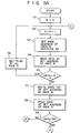
- step Sl a counter variable N is set to "0".
- the variable N indicates a page number being accessed.
- the variable N is incremented by one.
- step S3 in order to allow the CPU 14 to access a page N, a page address Al of the page N is set in the register 30 through the buses 19 and 20, the connector 21 and the bus 35.
- step S4 ID data is read out from a specific address of the page N, e.g., a start address.
- the CPU 14 transfers an address A2 for designating an address in the corresponding page to the decoder 32 through an address bus 36.
- the decoder 32 decodes the address A2 from the CPU 14 in accordance with the I/O select signal from the CPU 14, and supplies the clock pulse CK to the register 30 in accordance with the decoding result.
- the register 30 stores the page address Al from the CPU 14, and thereafter supplies it to the decoder 31.
- the decoder 31 decodes the page address Al from the register 30, and supplies the chip select signal CS to, e.g., the RAM 39.
- the CPU 14 reads out the ID data from the start address of the RAM 39 using the address A2.
- step S5 At a start address of each page, data indicating that the page is the RAM or ROM, data indicating the font stored in the page, and the like are stored. It is checked in step S5 if the data read out from the start address of the page is the ID data. That is, since the RAM may or may not be backed up with a battery, it is checked in step S5 whether or not the RAM is backed up with the battery. If YES in step S5, i.e., if the readout data is the ID data, a flag "B" indicating that the battery backed-up RAM is mounted in the page 1 area is written in the RAM 17 in step S6, and the flow returns to step S2.
- step S5 predetermined data "FO” (excluding "FF” in sexadecimal notation) is written at a predetermined address, e.g., the start address of the page 1 area, and thereafter the data is read out, as shown in steps S7 through S9. Then, it is checked if the readout data is the data "FF" in sexadecimal notation. In other words, the CPU 14 supplies a write signal to the RAM 39 through a memory read/write line 34 so as to write predetermined data therein. The reason for checking in step S9 if the readout data is "FF" is to check if a memory chip is mounted in the RAM 39 corresponding to the page 1 area.
- step S9 If data is read out from an address at which no memory chip is mounted, since the bus 35 is pulled up, data "FF" is obtained as if data "FF" were read out. If the readout data in step S9 is "FF", it is determined that the memory chip is not mounted. In step S10, a flag “RO” indicating no RAM is mounted in the page 1 area is written in the RAM 17. If NO in step S9, it is checked in step Sll if the readout data coincides with the data "FO” written in step S7. If YES in step Sll, a flag "Rl” indicating that a RAM is mounted in the page 1 area is written in the RAM 17.
- step Sll a flag "El" indicating that a RAM is mounted in the page 1 area but is malfunctioning is written in the RAM 17.
- step S15 it is detected whether or not a ROM is mounted in the page 3 to 8 areas in the ROM area. If YES in step S19 (if the ID data readout from the page N is the data "FF"), the flag "MO” which indicate that the ROM is not provided in the page N area, is written in the RAM 17 in step 20. If NO in step 21 (if the data readout from the page N is not the ID data), the flag "E2", indicating that the ROM provided in the page N operates erroneously, is written in the RAM 17 in step 22. If YES in step 21, the flag "Ml”, indicating that the ROM is provided in the page N area, is written in the RAM 17 in step 23.
- the CPU 14 switches memory access to the unit 22 side in accordance with a print character code supplied from the host computer.
- the CPU 14 sets a predetermined page address Al corresponding to the print character code in the register 30 through the buses 19 and 20, the connector 21 and the bus 35.
- the CPU 14 transfers a direct address A2 for designating an address in the page to the decoder 32 through the bus 36.
- the decoder 32 decodes the direct address from the CPU 14 in accordance with an I/O select signal received from the CPU 14 through the control signal line 33, and supplies the clock pulse CK to the register 30 in accordance with the decoding result.
- the register 30 stores the page address Al from the CPU 14 in synchronism with the clock pulse CK, and thereafter supplies it to the decoder 31.
- the decoder 31 decodes the page address Al from the register 30 and the direct address A2 from the CPU 14, and supplies the chip select signal CS to, e.g., the ROM 43.
- the ROM 43 having the storage area, e.g., page 7 and 8 areas storing high-density character pattern data corresponding to the print character code is selected.
- step S31 the CPU 14 accesses the ROM 43 using the page address Al, e.g., designating the page 7 and 8 areas and the direct address A2 designating the address in the corresponding pages, thereby reading out character pattern data constituting the predetermined high-density dot character pattern from the ROM 43.
- the CPU 14 supplies a read control signal RD to the ROM 43 through a memory read line 37, and reads out the character pattern data from the ROM 43 through the bus 35, the connector 21 and the buses 20 and 19.
- the CPU 14 writes the character pattern data read out from the ROM 43 in the storage area of the RAM 17 designated by the direct address A2, in step S32.
- the CPU 14 repeats the read operation of the character pattern data from the ROM 43 until the character pattern data for one character is read out and is stored in the RAM 17. This processing is repeated in accordance with discrimination of step S33 until the character pattern data for one character is read out from the ROM 43 and is stored in the RAM 17. Furthermore, the CPU 14 repeats the read operation from the ROM 43 in accordance with discrimination of step S34 until the character pattern data for one line is developed in the RAM 17.
- the CPU 14 switches page addresses required for reading out the character pattern data corresponding to the print chaarcter code (step S36).
- the CPU 14 switches the page address corresponding to, e.g., the page 7 area to that corresponding to, e.g., the page 8 area, and sets it in the register 30 shown in Fig. 4.
- the CPU 14 reads out the character pattern data stored in the page 8 area of the ROM 43, and stores it in the RAM 17.
- the CPU 14 reads out, e.g., the,high-density character pattern data corresponding to the print character code from the ROM 43 of the unit 22.
- the CPU 14 executes the printing operation in step S37.
- the CPU 14 supplies the print data including the character pattern data from the RAM 17 to the controller 18 in the same manner as in the dot printing operation of standard characters.
- the controller 18 controls the head 11 in accordance with the high-density character pattern from the register 23 shown in Fig. 2.
- the head 11 prints a character corresponding to the high-density character pattern data on the paper sheet.
- the CPU 14 recognizes a memory arrrangement in the unit 22 with respect to the ROMs 41 to 43 and the RAMs 39 and 40 in which a storage area is divided into page areas. Thus, the CPU 14 executes printing processing, e.g., as shown in Fig. 6 if the arrangement of the memory group in the unit 22 is as shown in Fig. 4. If the ROM 43 shown in Fig. 4 is not mounted, the CPU 14 interrupts readout of the character pattern data from the ROM 43, and executes processing indicating that printing of the character pattern data stored in the ROM 43 cannot be performed. When the RAMs 39 and 40 are not present, the CPU 14 interrupts the read/write operation with respect to the RAMs 39 and 40, and executes processing indicating that printing of character pattern data stored in the RAMs 39 and 40 cannot be performed.
- the CPU 14 at the printer side can recognize the storage area (page area) corresponding to the predetermined character pattern data in accordance with the arrangement of the memories in the unit 22. For this reason, when the ROMs 41 to 43 and the RAMs 39 and 40 are present in the unit 22 and the arrangement thereof is unknown, the CPU 14 at the printer side can recognize the storage area corresponding to the predetermined character pattern data. Therefore, characters other than the standard characters can be printed simply by loading the font cartridge unit to the printer main body.
Landscapes
- Physics & Mathematics (AREA)
- Engineering & Computer Science (AREA)
- Mathematical Physics (AREA)
- General Engineering & Computer Science (AREA)
- General Physics & Mathematics (AREA)
- Theoretical Computer Science (AREA)
- Record Information Processing For Printing (AREA)
- Dot-Matrix Printers And Others (AREA)
Applications Claiming Priority (2)
| Application Number | Priority Date | Filing Date | Title |
|---|---|---|---|
| JP59181871A JPS6158749A (ja) | 1984-08-31 | 1984-08-31 | 印字処理装置 |
| JP181871/84 | 1984-08-31 |
Publications (3)
| Publication Number | Publication Date |
|---|---|
| EP0173285A2 true EP0173285A2 (de) | 1986-03-05 |
| EP0173285A3 EP0173285A3 (en) | 1986-07-16 |
| EP0173285B1 EP0173285B1 (de) | 1989-08-16 |
Family
ID=16108303
Family Applications (1)
| Application Number | Title | Priority Date | Filing Date |
|---|---|---|---|
| EP85110701A Expired EP0173285B1 (de) | 1984-08-31 | 1985-08-26 | Punktmatrixdrucker mit Schriftarten-Modulen |
Country Status (4)
| Country | Link |
|---|---|
| US (1) | US4660999A (de) |
| EP (1) | EP0173285B1 (de) |
| JP (1) | JPS6158749A (de) |
| DE (1) | DE3572412D1 (de) |
Cited By (3)
| Publication number | Priority date | Publication date | Assignee | Title |
|---|---|---|---|---|
| EP0311111A2 (de) * | 1987-10-08 | 1989-04-12 | Advanced Micro Devices, Inc. | Gerät zur Sammlung von Daten zur Zuführung an einem Ausgangsabtaster |
| EP0317996A2 (de) * | 1987-11-25 | 1989-05-31 | Oki Electric Industry Company, Limited | Drucker |
| EP0388160A2 (de) * | 1989-03-15 | 1990-09-19 | Canon Kabushiki Kaisha | Ausgabevorrichtung |
Families Citing this family (31)
| Publication number | Priority date | Publication date | Assignee | Title |
|---|---|---|---|---|
| FR2566327B1 (fr) * | 1984-06-25 | 1989-06-02 | Epson Corp | Imprimante |
| US4730947A (en) * | 1985-08-19 | 1988-03-15 | Citizen Watch Co., Ltd. | Printer having a control circuit section of cassette type |
| JPH073631B2 (ja) * | 1986-02-05 | 1995-01-18 | ミノルタ株式会社 | フォントカートリッジとそのデータ管理方法 |
| US5345518A (en) * | 1986-04-24 | 1994-09-06 | Canon Kabushiki Kaisha | Pattern generator |
| JPH0737155B2 (ja) * | 1986-10-07 | 1995-04-26 | シチズン時計株式会社 | プリンタ |
| US4942390A (en) * | 1987-04-01 | 1990-07-17 | International Business Machines Corporation | Method and apparatus for generating a character image |
| US5171092A (en) * | 1987-07-06 | 1992-12-15 | Canon Kabushiki Kaisha | Printing apparatus that stores externally supplied fonts |
| US5242230A (en) * | 1987-07-06 | 1993-09-07 | Canon Kabushiki Kaisha | Font cartridge with thermal correction information |
| US5142613A (en) * | 1987-07-23 | 1992-08-25 | Minolta Camera Kabushiki Kaisha | Font managing apparatus for a character generator |
| JPH0786829B2 (ja) * | 1987-07-31 | 1995-09-20 | 株式会社東芝 | 電子機器装置 |
| US4992827A (en) * | 1987-12-28 | 1991-02-12 | Canon Kabushiki Kaisha | Image forming apparatus |
| JPH0818444B2 (ja) * | 1988-08-19 | 1996-02-28 | キヤノン株式会社 | 印刷装置 |
| US4908637A (en) * | 1989-01-30 | 1990-03-13 | Acer Incorporated | Font cartridge adapter |
| JP2745669B2 (ja) * | 1989-04-27 | 1998-04-28 | ブラザー工業株式会社 | プリンタ |
| JPH0325523A (ja) * | 1989-06-22 | 1991-02-04 | Ricoh Co Ltd | コンピユータ周辺機器 |
| JPH03288926A (ja) | 1990-04-05 | 1991-12-19 | Canon Inc | 画像出力装置 |
| US5187664A (en) * | 1990-11-27 | 1993-02-16 | Eaton-Kenway, Inc. | Proportional position-sensing system for an automatic guided vehicle |
| US5150456A (en) * | 1990-08-06 | 1992-09-22 | Elite High Technology, Inc. | Graphic image printing system and method |
| US5255360A (en) * | 1990-09-14 | 1993-10-19 | Hughes Aircraft Company | Dual programmable block texturing and complex clipping in a graphics rendering processor |
| US5206736A (en) * | 1990-09-28 | 1993-04-27 | Xerox Corporation | Font storage management and control |
| US5167013A (en) * | 1990-09-28 | 1992-11-24 | Xerox Corporation | User definable font substitutions with equivalency indicators |
| KR930011662B1 (ko) * | 1990-11-30 | 1993-12-16 | 현대전자산업 주식회사 | 카트리지를 이용한 lbp 시스팀 |
| US6948006B1 (en) * | 1990-12-12 | 2005-09-20 | Canon Kabushiki Kaisha | Host system that provides device driver for connected external peripheral if device driver type is available or device driver is downloaded from memory of external peripheral to host system |
| US5095449A (en) * | 1990-12-24 | 1992-03-10 | Stephen Kurtin | Expansion module for computer printer font cartridge |
| DE69132636T2 (de) * | 1991-08-19 | 2002-04-18 | Oki America Inc | Multifunktionelles Dokumentenverarbeitungssystem |
| JP2556224B2 (ja) * | 1991-09-25 | 1996-11-20 | ブラザー工業株式会社 | テープ印字装置 |
| US5193052A (en) * | 1991-11-07 | 1993-03-09 | Advanced Matrix Technology, Inc. | Font cartridge extender with spring hook latch |
| EP0586080B1 (de) * | 1992-07-31 | 1999-10-06 | Canon Kabushiki Kaisha | Bildverarbeitungsverfahren und -gerät |
| US5990907A (en) * | 1995-12-15 | 1999-11-23 | Colletti; John C. | Automatic font management within an operating system environment |
| JPH10208463A (ja) * | 1997-01-22 | 1998-08-07 | Nec Corp | メモリ実装判別回路 |
| US7116440B2 (en) * | 2003-02-28 | 2006-10-03 | Aperio Technologies, Inc. | Image processing and analysis framework |
Citations (4)
| Publication number | Priority date | Publication date | Assignee | Title |
|---|---|---|---|---|
| US4031519A (en) * | 1974-11-11 | 1977-06-21 | Ibm Corporation | Printer |
| US4179732A (en) * | 1977-06-10 | 1979-12-18 | Dataproducts Corporation | Microprogrammable processor control printer system |
| EP0072708A2 (de) * | 1981-08-19 | 1983-02-23 | Fuji Xerox Co., Ltd. | Drucker |
| JPS5971882A (ja) * | 1982-10-18 | 1984-04-23 | Konishiroku Photo Ind Co Ltd | プリンタ |
Family Cites Families (6)
| Publication number | Priority date | Publication date | Assignee | Title |
|---|---|---|---|---|
| US4159541A (en) * | 1977-07-01 | 1979-06-26 | Ncr Corporation | Minimum pin memory device |
| US4452136A (en) * | 1979-10-19 | 1984-06-05 | International Business Machines Corporation | Printer subsystem with dual cooperating microprocessors |
| US4281938A (en) * | 1980-01-14 | 1981-08-04 | Phillips Stephen R | Automatic print wheel element changing mechanism for a serial printer |
| CA1162317A (en) * | 1980-04-28 | 1984-02-14 | Gordon Sohl | Read only memory coded print wheel cartridge |
| US4388010A (en) * | 1980-12-31 | 1983-06-14 | International Business Machines Corporation | Font module for matrix printer |
| IT8253961V0 (it) * | 1982-11-18 | 1982-11-18 | Olivetti & Co Spa | Modulo di memoria in cassetta e dispositivo per il suo collegamento alla circuiteria di una macchina per scrivere elettronica |
-
1984
- 1984-08-31 JP JP59181871A patent/JPS6158749A/ja active Pending
-
1985
- 1985-08-26 DE DE8585110701T patent/DE3572412D1/de not_active Expired
- 1985-08-26 EP EP85110701A patent/EP0173285B1/de not_active Expired
- 1985-08-30 US US06/770,995 patent/US4660999A/en not_active Expired - Fee Related
Patent Citations (4)
| Publication number | Priority date | Publication date | Assignee | Title |
|---|---|---|---|---|
| US4031519A (en) * | 1974-11-11 | 1977-06-21 | Ibm Corporation | Printer |
| US4179732A (en) * | 1977-06-10 | 1979-12-18 | Dataproducts Corporation | Microprogrammable processor control printer system |
| EP0072708A2 (de) * | 1981-08-19 | 1983-02-23 | Fuji Xerox Co., Ltd. | Drucker |
| JPS5971882A (ja) * | 1982-10-18 | 1984-04-23 | Konishiroku Photo Ind Co Ltd | プリンタ |
Non-Patent Citations (2)
| Title |
|---|
| IBM TECHNICAL DISCLOSURE BULLETIN, vol. 15, no. 2, July 1972, pages 492-493, New York, US; J.A. ERICKSON: "Extended print character set" * |
| PATENTS ABSTRACTS OF JAPAN, vol. 8, no. 180 (M-318) [1617], 18th August 1984; & JP-A-59 071 882 (KONISHIROKU SHASHIN KOGYO K.K.) 23-04-1984 * |
Cited By (7)
| Publication number | Priority date | Publication date | Assignee | Title |
|---|---|---|---|---|
| EP0311111A2 (de) * | 1987-10-08 | 1989-04-12 | Advanced Micro Devices, Inc. | Gerät zur Sammlung von Daten zur Zuführung an einem Ausgangsabtaster |
| EP0311111A3 (de) * | 1987-10-08 | 1990-10-24 | Advanced Micro Devices, Inc. | Gerät zur Sammlung von Daten zur Zuführung an einem Ausgangsabtaster |
| EP0317996A2 (de) * | 1987-11-25 | 1989-05-31 | Oki Electric Industry Company, Limited | Drucker |
| EP0317996A3 (de) * | 1987-11-25 | 1991-09-18 | Oki Electric Industry Company, Limited | Drucker |
| EP0388160A2 (de) * | 1989-03-15 | 1990-09-19 | Canon Kabushiki Kaisha | Ausgabevorrichtung |
| EP0388160A3 (de) * | 1989-03-15 | 1991-01-02 | Canon Kabushiki Kaisha | Ausgabevorrichtung |
| US5355231A (en) * | 1989-03-15 | 1994-10-11 | Canon Kabushiki Kaisha | Output apparatus with dot density adjustments |
Also Published As
| Publication number | Publication date |
|---|---|
| DE3572412D1 (en) | 1989-09-21 |
| US4660999A (en) | 1987-04-28 |
| JPS6158749A (ja) | 1986-03-26 |
| EP0173285B1 (de) | 1989-08-16 |
| EP0173285A3 (en) | 1986-07-16 |
Similar Documents
| Publication | Publication Date | Title |
|---|---|---|
| EP0173285B1 (de) | Punktmatrixdrucker mit Schriftarten-Modulen | |
| EP0173287B1 (de) | Punktmatrixdrucker mit Zeichensatzpatrone | |
| US4686525A (en) | Image data output apparatus | |
| EP0082297B1 (de) | Drucken von Punktmatrixzeichen mit eingeschränktem Speicher | |
| KR930000488B1 (ko) | 실제적인 장착위치와는 무관하게 폰트 메모리를 지정할 수 있는 인자장치와 그 지정방법 | |
| US4926347A (en) | Printer with emulation card installation reporting feature | |
| JPS60116464A (ja) | プリンタ | |
| JPS62182795A (ja) | フォントカートリッジとそのデータ管理方法 | |
| US4480316A (en) | Ruled line print control system in a word processing apparatus | |
| US5257388A (en) | Device for detecting whether an attached external memory stores valid data, if not, whether the external memory is capable of storing data | |
| EP0317996B1 (de) | Drucker | |
| CA1236587A (en) | Dot-matrix printer with font cartridge unit | |
| US5671339A (en) | Output apparatus | |
| JPH01235658A (ja) | 印字装置 | |
| CN85107217A (zh) | 具有字体盒式存贮器的点阵打印机 | |
| JPH02283466A (ja) | プリンタ | |
| EP0443183B1 (de) | Verfahren und System zur Aufzeichnung von und zum Zugang zu Schrifttypenzeichendaten eines Laserdruckers | |
| JPS6319277A (ja) | 印刷装置 | |
| EP0582794A1 (de) | Elektronische Schreibmaschine mit Prüfung der Rechtschreibung | |
| JPH01214460A (ja) | プリンタのページ出力検出方式 | |
| JPS635767B2 (de) | ||
| JPS6371357A (ja) | 印字出力制御装置 | |
| JPH0816866B2 (ja) | 出力装置 | |
| JPH03221481A (ja) | シリアル記録装置 | |
| JPS61274953A (ja) | ドツトマトリツクスプリンタ |
Legal Events
| Date | Code | Title | Description |
|---|---|---|---|
| PUAI | Public reference made under article 153(3) epc to a published international application that has entered the european phase |
Free format text: ORIGINAL CODE: 0009012 |
|
| 17P | Request for examination filed |
Effective date: 19850923 |
|
| AK | Designated contracting states |
Kind code of ref document: A2 Designated state(s): DE FR GB |
|
| PUAL | Search report despatched |
Free format text: ORIGINAL CODE: 0009013 |
|
| AK | Designated contracting states |
Kind code of ref document: A3 Designated state(s): DE FR GB |
|
| 17Q | First examination report despatched |
Effective date: 19881128 |
|
| GRAA | (expected) grant |
Free format text: ORIGINAL CODE: 0009210 |
|
| AK | Designated contracting states |
Kind code of ref document: B1 Designated state(s): DE FR GB |
|
| REF | Corresponds to: |
Ref document number: 3572412 Country of ref document: DE Date of ref document: 19890921 |
|
| ET | Fr: translation filed | ||
| PLBI | Opposition filed |
Free format text: ORIGINAL CODE: 0009260 |
|
| 26 | Opposition filed |
Opponent name: N.V. PHILIPS' GLOEILAMPENFABRIEKEN Effective date: 19900515 |
|
| PGFP | Annual fee paid to national office [announced via postgrant information from national office to epo] |
Ref country code: FR Payment date: 19920807 Year of fee payment: 8 |
|
| PGFP | Annual fee paid to national office [announced via postgrant information from national office to epo] |
Ref country code: GB Payment date: 19920814 Year of fee payment: 8 |
|
| PLBN | Opposition rejected |
Free format text: ORIGINAL CODE: 0009273 |
|
| STAA | Information on the status of an ep patent application or granted ep patent |
Free format text: STATUS: OPPOSITION REJECTED |
|
| 27O | Opposition rejected |
Effective date: 19920612 |
|
| PG25 | Lapsed in a contracting state [announced via postgrant information from national office to epo] |
Ref country code: GB Effective date: 19930826 |
|
| PGFP | Annual fee paid to national office [announced via postgrant information from national office to epo] |
Ref country code: DE Payment date: 19940214 Year of fee payment: 9 |
|
| GBPC | Gb: european patent ceased through non-payment of renewal fee |
Effective date: 19930826 |
|
| PG25 | Lapsed in a contracting state [announced via postgrant information from national office to epo] |
Ref country code: FR Effective date: 19940429 |
|
| REG | Reference to a national code |
Ref country code: FR Ref legal event code: ST |
|
| PG25 | Lapsed in a contracting state [announced via postgrant information from national office to epo] |
Ref country code: DE Effective date: 19950503 |