EP0169915B1 - Digitaler Phasendemodulator - Google Patents
Digitaler Phasendemodulator Download PDFInfo
- Publication number
- EP0169915B1 EP0169915B1 EP84106475A EP84106475A EP0169915B1 EP 0169915 B1 EP0169915 B1 EP 0169915B1 EP 84106475 A EP84106475 A EP 84106475A EP 84106475 A EP84106475 A EP 84106475A EP 0169915 B1 EP0169915 B1 EP 0169915B1
- Authority
- EP
- European Patent Office
- Prior art keywords
- output
- input
- changeover switch
- stage
- adder
- Prior art date
- Legal status (The legal status is an assumption and is not a legal conclusion. Google has not performed a legal analysis and makes no representation as to the accuracy of the status listed.)
- Expired
Links
Images
Classifications
-
- G—PHYSICS
- G06—COMPUTING OR CALCULATING; COUNTING
- G06F—ELECTRIC DIGITAL DATA PROCESSING
- G06F7/00—Methods or arrangements for processing data by operating upon the order or content of the data handled
- G06F7/38—Methods or arrangements for performing computations using exclusively denominational number representation, e.g. using binary, ternary, decimal representation
- G06F7/48—Methods or arrangements for performing computations using exclusively denominational number representation, e.g. using binary, ternary, decimal representation using non-contact-making devices, e.g. tube, solid state device; using unspecified devices
- G06F7/544—Methods or arrangements for performing computations using exclusively denominational number representation, e.g. using binary, ternary, decimal representation using non-contact-making devices, e.g. tube, solid state device; using unspecified devices for evaluating functions by calculation
- G06F7/5446—Methods or arrangements for performing computations using exclusively denominational number representation, e.g. using binary, ternary, decimal representation using non-contact-making devices, e.g. tube, solid state device; using unspecified devices for evaluating functions by calculation using crossaddition algorithms, e.g. CORDIC
-
- H—ELECTRICITY
- H03—ELECTRONIC CIRCUITRY
- H03D—DEMODULATION OR TRANSFERENCE OF MODULATION FROM ONE CARRIER TO ANOTHER
- H03D3/00—Demodulation of angle-, frequency- or phase- modulated oscillations
- H03D3/006—Demodulation of angle-, frequency- or phase- modulated oscillations by sampling the oscillations and further processing the samples, e.g. by computing techniques
Definitions
- Such an arrangement is, in principle, described in US-A-4 090 145.
- the required memory space of the read-only memory depends on the proposed resolution of the resolution of the analog-digital converter, ie. H. on the number of digits n of the digital signals to be processed; namely 2 "n memory locations (bit) are required.
- the invention characterized in the claims is therefore based on the object, based on the prior art mentioned at the outset, of specifying a digital phase demodulator which inserts digital signals with a number of digits. allowed greater than 10 without demodulating the large storage space requirement of the read-only memory.
- the above-mentioned, appropriately conditioned quadrant signals x ', y' are used as input signals, which can be generated, for example, in accordance with the arrangement specified in the above-mentioned US patent.
- the generation of the arc tangent signal corresponding to the quotient y '/ x', that is to say the angle between the abscissa and the vector formed by x ', y' in the x'-y 'coordinate system thus covers its first half quadrant, that is to say the angle between 0 and 45 °. Due to the periodicity of the tangent function, the corresponding output signals dp can also be generated for larger angles than 45 ° by means of the conditioning circuit described above.
- the first solution variant according to FIG. 1 consists of n-1 similar stages s1, s2, sn-1 and the nth stage sn, the structure of which differs slightly from that of the other stages.
- the maximum number of predetermined positions of one of the quadrant signals x ', y' is designated by n.
- Each of the similar stages s1 ... sn-1 consists of the adder ad, the subtractor sb, the first and the second constant multiplier m1, m2 for the factor 2- r , where r is 1 ...
- n-1 from the first, the second and the third electronic changeover switch u1, u2, u3 as well as the read-only memory rm1 for arctan 2 -r , ie a read-only memory requiring a correspondingly small amount of semiconductor body area is to be provided in each stage only for the sole arctangent value 2 " .
- the quadrant signal x 'or in each further stage s2 ... sn-1 is the output of the first switch u1 belonging to the previous stage at the respective first input of the adder ad, the first constant multiplier m1 and the first switch u1 connected to this stage.
- the output of the second switch u2 belonging to the preceding stage is at the input of the second constant multiplier m2 of this stage and at the first input of the second switch u2 and at the minus input m of the subtractor sb.
- the output of the second constant multiplier m2 is connected to the second input of the adder ad and the output of the first constant multiplier m1 to the subtractor input s of the subtractor sb.
- the output of the adder ad is at the second input of the first switch u1 and the output of the subtractor sb is at the second input of the second switch u2, while the first input of the third switch u3 is at the number zero “0” and its second input is at the output of the read-only memory rm1 and its output one of the n inputs of the multiple adder ma is connected.
- the sign output sg of the subtractor sb is in each stage at the respective control input of the three changeover switches u1. u2, u3, and the switching assignment is selected so that the respective first input is switched through if the sign is negative and the respective second input is switched through to the respective output if the sign is positive.
- the nth stage sn consists of the further constant multiplier mn for the factor 2 -n , the input of which is at the output of the first switch u1 of the (n-1) th stage sn-1, of the further subtractor sbn, the minute input m at the output of the second switch u2 of the preceding stage sn-1 and its subtrahend input s is at the output of the further constant multiplier mn, further from the further switch un, the first input of which is supplied with the number zero 0 0, and finally from the read-only memory rmn for arctan 2 -n , whose output is connected to the second input of the further switch un, whose output is connected in turn to the multiple adder ma and whose control input is connected to the sign output sg of the further subtractor sbn.
- the second solution variant according to FIG. 2 differs from the first according to FIG. 1 essentially in that from a step j + 1, where j can be an integer between 4 and 8, the read-only memory rm1 according to FIG. 1 is omitted. since for arguments 2 -j the associated tangent value can be replaced by the argument itself with sufficient accuracy.
- the first j stages of the arrangement according to FIG. 2 are therefore constructed identically to the corresponding stages s1 ... sn-1 of the arrangement according to FIG. 1, only the subtractor sb according to FIG. 1 now being the first subtractor sb1 according to FIG. 2 is defined.
- the second solution variant according to FIG. 2 contains n-j-1 identical cells and instead of the nth stage according to FIG. 1 the (n-j) th cell zn. Furthermore, the (n-j) stage register rg is provided, the parallel output of which leads to one of the inputs of the multiple adder ma. Compared to the arrangement according to FIG. 1, according to which it has n inputs and thus has to carry out n-1 additions, this only has j + I inputs for j additions and is therefore smaller in terms of semiconductor body space than in FIG. 1.
- r ' is equal to j + 1
- the switching assignment is selected such that if the sign at the sign output sg of the two subtractors sb1, sb2 is negative, the respective first input or, if the sign is positive, the respective second input of the assigned changeover switches u1, u2, u3 (in stages s1 ... sj) or u4 (in the cells) is switched through to the respective output.
- the (nj) th cell zn consists of the further constant multiplier mn for the factor 2- n , the input of which is at the output of the first switch u1 of the jth stage sj; further from the further subtractor sbn, whose minus input m is at the output of the fourth switch u4 of the preceding cell and whose subtractor input s is at the output of the further constant multiplier mn; and finally from the further inverter ivn with its input at the sign output sg of the further subtractor sbn.
- the respective output of all inverters iv, ivn lies, depending on its value, at the associated step input of the register rg and its parallel output at one of the inputs of the multiple adder ma, at whose output the digital phase-demodulated signal dp occurs, which occurs in the first half quadrant of the x'-y ' Coordinate system, i.e. between 0 ° and 45 °.
- the connecting lines are drawn only as simple lines, regardless of the circuitry implementation. However, this is not intended to imply any restriction in that the quadrant signals x ', y' are also processed in parallel.
- the connecting lines are then the usual buses, the number of parallel lines of which is adapted to the number of digits n of the digital words to be processed.
- the corresponding adders, subtractors, multipliers and switches are also corresponding parallel processing units. Such an implementation will otherwise be provided when fast signal processing is required, the overall arrangement then being carried out using the so-called pipeline technology.
- the two solution variants of the invention can also be simplified by using multiplex technology, i. H. the total number of stages or cells is smaller than the number of digits n of the quadrant signals x ', y' and the cells are run through several times during a processing cycle.
- the invention is suitable for implementation as an integrated circuit, in particular in the form of the so-called MOS circuits, that is to say as an insulating layer field-effect transistor circuit.
- Demodulation in the radio stereo system (amplitude-modulated system) standardized in the USA, television sound demodulation and FM radio demodulation are to be mentioned as special fields of application of the invention in the audio field.
- the invention can also be used in SECAM chrominance demodulation and in magnetic image recording; e.g. B. in VCRs can be applied.
Landscapes
- Engineering & Computer Science (AREA)
- Theoretical Computer Science (AREA)
- General Physics & Mathematics (AREA)
- Physics & Mathematics (AREA)
- Computational Mathematics (AREA)
- Computing Systems (AREA)
- Power Engineering (AREA)
- Mathematical Analysis (AREA)
- Mathematical Optimization (AREA)
- Pure & Applied Mathematics (AREA)
- General Engineering & Computer Science (AREA)
- Complex Calculations (AREA)
- Measuring Phase Differences (AREA)
- Digital Transmission Methods That Use Modulated Carrier Waves (AREA)
Description
- Die Erfindung betrifft einen digitalen Phasendemodulator mit einem von einem Taktsignal getakteten Analog-Digital-Wandler für die Umwandlung des zu demodulierenden Analogsignals in ein Digitalsignal, mit einem digitalen 90°-Phasenschieber ( = Hilbert-Transformator = Quadratursignal- Generator), dem das Digitalsignal zur Bildung des Quadratursignals zugeführt ist, mit einer Kondltionierschaltung für Digital- und Quadratursignal, an deren Ausgang entsprechende, zum ersten x'-y'-Koordinatensystem-Halbquadranten gehörende digitale Quadrantsignale x', y' entstehen, und mit einer die Arcus-Tangens- Funktion des Quotienten y'/x' liefernden, einen Festwertspeicher enthaltenden Schaltung, vgl. den jeweiligen Oberbegriff der Ansprüche 1 und 2. Eine derartige Anordnung ist, was das Prinzip betrifft, in der US-A-4 090 145 beschrieben.
- Der benötigte Speicherplatz des Festwertspeichers hängt bei der vorbeschriebenen Anordnung vom vorgesehenen Auflösungsvermögen des Analog-Digital-Wandlers, d. h. von der Stellenzahl n der zu verarbeitenden Digitalsignale ab ; es werden nämlich 2"n Speicherplätze (Bit) benötigt.
- Für die digitale Signalverarbeitung von Videosignalen mit n = 6...8 Stellen sind also 27 bis 29 Speicherplätze des Festwertspeichers erforderlich, welche Forderung mit den heutigen Mitteln der Halbleitertechnik ohne weiteres erfüllt werden kann. Digitalsignale mit größeren Stellenzahlen, z. B. n = 13...17, wie sie z. B. für die digitale Signalverarbeitung von Audiosignalen erwünscht sind, führen jedoch zu einem Speicherplatzbedarf von 214...218 Bit, was mit den heutigen Mitteln der Halbleitertechnik nur zu einer unrealistischen, d. h. mit vertretbarem Aufwand nicht realisierbaren Halbleiterkörper-Größe einer den digitalen Phasendemodulator enthaltenden integrierten Schaltung führt. Der in den Ansprüchen gekennzeichneten Erfindung liegt somit die Aufgabe zugrunde, ausgehend von dem eingangs genannten Stand der Technik, einen digitalen Phasendemodulator anzugeben, der Digitalsignale mit einer Stellenanzahl insles. größer 10 ohne den geschilderten großen Speicherplatzbedarf des Festwertspeichers zu demodulieren gestattet.
- Der wesentliche Vorteil der Erfindung ist darin zu sehen, daß bei der einen Lösungsvarianten wie sie im Anspruch 1 angegeben ist, nur noch n2 Speicherplätze, zudem verteilt auf n kleine Festwertspeicher, benötigt werden und daß sich dieser Speicherplatzbedarf bei der zweiten Lösungsvariante, wie sie im Anspruch 2 angegeben ist, nochmals auf ein Viertel bis die Hälfte reduziert.
- Die Erfindung und weitere Vorteile werden nun anhand der Figuren der Zeichnung näher erläutert.
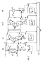
- Fig. 1 zeigt schematisch in Form eines Blockschaltbilds ein Ausführungsbeispiel der ersten Lösungsvariante der Erfindung, und
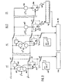
- Fig. 2 zeigt in gleicher Weise das Schaltbild eines Ausführungsbeispiels der zweiten Lösungsvariante der Erfindung.
- Die in Form eines schematischen Blockschaltbilds aufgebaute Fig. 1 zeigt ein Ausführungsbeispiel der ersten Lösungsvariante der Erfindung. Als Eingangssignale dienen die oben erwähnten, entsprechend konditionierten Quadrantsignale x', y' die beispielsweise entsprechend der in der eingangs genannten US-Patentschrift angegebenen Anordnung erzeugt werden können. Die Erzeugung des dem Quotienten y'/x' entsprechenden Arcus-Tangens-Signals also des Winkels zwischen der Abszisse und dem von x', y' gebildeten Vektor im x'-y'-Koordinatensystem, erfaßt somit dessen ersten Halbquadranten, also Winkel zwischen 0 und 45°. Aufgrund der Periodizität der Tangensfunktion können mittels der vorbeschriebenen Konditionierschaltung auch die entsprechenden Ausgangssignale dp für größere Winkel als 45° erzeugt werden.
- Die erste Lösungsvariante nach Fig. 1 besteht aus n-1 gleichartigen Stufen s1, s2, sn-1 sowie der n-ten Stufe sn, deren Aufbau von denen der anderen Stufen geringfügig abweicht. Mit n ist die maximale Anzahl der vorgegebenen Stellen eines der Quadrantsignale x', y' bezeichnet. Von den gleichartigen Stufen s1...sn-1 besteht jede aus dem Addierer ad, dem Subtrahierer sb, dem ersten und dem zweiten Konstantenmultiplizierer m1, m2 für den Faktor 2-r, wobei r gleich 1...n-1 ist, aus dem ersten, dem zweiten und dem dritten elektronischen Umschalter u1, u2, u3 sowie dem Festwertspeicher rm1 für arctan 2-r, d. h. es ist lediglich für den alleinigen Arcus-Tangens-Wert 2" in jeder Stufe ein entsprechend wenig Halbleiterkörperfläche erfordernder Festwertspeicher vorzusehen.
- In der ersten Stufe s1 ist das Quadrantsignal x' bzw. in jeder weiteren Stufe s2...sn-1 der Ausgang des zur vorangehenden Stufe gehörenden ersten Umschalters u1 am jeweiligen ersten Eingang des Addierers ad, des ersten Konstantenmultiplizierers m1 und des ersten Umschalters u1 dieser Stufe angeschlossen.
- In der ersten Stufe s1 liegt das zweite Quadrantsignal y' bzw. in jeder weiteren Stufe s2...sn-1 der Ausgang des zur vorangehenden Stufe gehörenden zweiten Umschalters u2 am Eingang des zweiten Konstantenmultiplizierers m2 dieser Stufe und am ersten Eingang des zweiten Umschalters u2 sowie am Minuendeingang m des Subtrahierers sb. Der Ausgang des zweiten Konstantenmultiplizierers m2 ist mit dem zweiten Eingang des Addierers ad und der Ausgang des ersten Konstantenmultiplizierers m1 mit dem Subtrahendeingang s des Subtrahierers sb verbunden. Der Ausgang des Addierers ad liegt am zweiten Eingang des ersten Umschalters u1 und der Ausgang des Subtrahierers sb am zweiten Eingang des zweiten Umschalters u2, während der erste Eingang des dritten Umschalters u3 an der Zahl Null « 0 » und sein zweiter Eingang am Ausgang des Festwertspeichers rm1 sowie sein Ausgang an einem der n Eingänge des Mehrfachaddierers ma angeschlossen ist. Der Vorzeichenausgang sg des Subtrahierers sb liegt in jeder Stufe am jeweiligen Steuereingang der drei Umschalter u1. u2, u3, und die Schaltzuordnung ist so gewählt, daß bei negativem Vorzeichen der jeweilige erste Eingang und bei positivem Vorzeichen der jeweilige zweite Eingang zum jeweiligen Ausgang durchgeschaltet ist.
- Die n-te Stufe sn besteht aus dem weiteren Konstäntenmultiplizierer mn für den Faktor 2-n, dessen Eingang am Ausgang des ersten Umschalters u1 der (n-1)-ten Stufe sn-1 liegt, aus dem weiteren Subtrahierer sbn, dessen Minuendeingang m am Ausgang des zweiten Umschalters u2 der vorausgehenden Stufe sn-1 und dessen Subtrahend-Eingang s am Ausgang des weiteren Konstantenmültiplizierers mn liegt, ferner aus dem weiteren Umschalter un, dessen erstem Eingang die Zahl Null 0 0 zugeführt ist, und schließlich aus dem Festwertspeicher rmn für arctan 2-n, dessen Ausgang mit dem zweiten Eingang des weiteren Umschalters un verbunden ist, dessen Ausgang hinwiederum am Mehrfachaddierer ma und dessen Steuereingang am Vorzeichenausgang sg des weiteren Subtrahierers sbn angeschlossen ist.
- Die zweite Lösungsvariante nach Fig. 2 unterscheidet sich von der ersten nach Fig. 1 im wesentlichen darin, daß ab einer Stufe j + 1, wobei j eine ganze Zahl zwischen 4 und 8 sein kann, der Festwertspeicher rm1 nach Fig. 1 weggelassen ist, da-für Argumente 2-j der zugehörige Tangenswert durch das Argument selbst mit ausreichender Genauigkeit ersetzt werden kann. Die ersten j Stufen der Anordnung nach Fig. 2 sind daher identisch aufgebaut wie die entsprechenden Stufen s1...sn-1 der Anordnung nach Fig. 1, wobei lediglich der Subtrahierer sb nach Fig. 1 nunmehr als erster Subtrahierer sb1 nach Fig. 2 definiert ist.
- Anstatt der n-j-1 gleichartigen Stufen nach Fig. 1 enthält die zweite Lösungsvariante nach Fig. 2 ' n-j-1 gleichartige Zellen und anstatt der n-ten Stufe nach Fig. 1 die (n-j)-te Zelle zn. Ferner ist das (n-j)-stufige Register rg vorgesehen, dessen Parallelausgang zu einem der Eingänge des Mehrfachaddierers ma führt. Dieser hat also gegenüber der Anordnung nach Fig. 1, wonach er n Eingänge hat und somit n-1 Additionen auszuführen hat, nur noch j+I Eingänge für j Additionen und ist somit von geringerem Halbleiterkörper-Platzbedarf als in Fig. 1.
- Die gleichartigen Zellen, von der in Fig. 2 die Zelle sj+1 gezeigt ist, bestehen jeweils aus dem dritten Konstantenmultiplizierer m3 für den Faktor 2-r, dessen Eingang am Ausgang des ersten Umschalters u1 der j-ten Stufe sj liegt ; ferner aus dem vierten Umschalter u4, dessen erster Eingang in der (j + 1) ten Zelle am Ausgang des zweiten Umschalters u2 der j-ten Stufe sj bzw. in jeder weiteren Zelle am Ausgang des vierten Umschalters u4 der vorangehenden Zelle liegt ; ferner aus dem zweiten Subtrahierer sb2, dessen Minuendeingang m am ersten Eingang des vierten Umschalters u4, dessen Subtrahendeingang s am Ausgang des dritten Konstantenmultiplizierers m3, dessen Ausgang am zweiten Eingang des vierten Umschalters u4 und dessen Vorzeichenausgang sg am Steuereingang des vierten Umschalters u4 liegt ; und schließlich aus dem Inverter iv, dessen Eingang mit dem Vorzeichenausgang sg des vierten Umschalters u4 verbunden ist. r' ist dabei gleich j + 1...n-1.
- Auch bei dieser Lösungsvariante ist wie bei der nach Fig. 1 die Schaltzuordnung so gewählt, daß bei negativem Vorzeichen am Vorzeichenausgang sg der beiden Subtrahierer sb1, sb2 der jeweilige erste Eingang bzw. bei positivem Vorzeichen der jeweilige zweite Eingang der zugeordneten Umschalter u1, u2, u3 (in den Stufen s1...sj) bzw. u4 (in den Zellen) zum jeweiligen Ausgang durchgeschaltet ist.
- Die (n-j)-te Zelle zn besteht aus dem weiteren Konstantenmultiplizierer mn für den Faktor 2-n, dessen Eingang am Ausgang des ersten Umschalters u1 der j-ten Stufe sj liegt ; ferner aus dem weiteren Subtrahierer sbn, dessen Minuendeingang m am Ausgang des vierten Umschalters u4 der vorausgehenden Zelle und dessen Subtrahendeingang s am Ausgang des weiteren Konstantenmultiplizierers mn liegt ; und schließlich aus dem weiteren mit seinem Eingang am Vorzeichenausgang sg des weiteren Subtrahierers sbn liegenden Inverter ivn.
- Der jeweilige Ausgang aller Inverter iv, ivn liegt entsprechend seiner Wertigkeit am zugehörigen Stufeneingang des Registers rg und dessen Parallelausgang an einem der Eingänge des Mehrfachaddierers ma, an dessen Ausgang wiederum das digitale phasendemodulierte Signal dp auftritt, das im ersten Halbquadranten des x'-y'-Koordinatensystems, also zwischen 0° und 45° liegt.
- In den Figuren der Zeichnung sind unabhängig von der schaltungstechnischen Realisierung die Verbindungsleitungen lediglich als einfache Leitungen gezeichnet. Dies soll jedoch keine Einschränkung dahingehend bedeuten, daß auch eine parallele Signalverarbeitung der Quadrantsignale x', y' vorgenommen wird. In einem solchen Fall sind die Verbindungsleitungen dann die üblichen Busse, deren Anzahl an parallelen Leitungen der Stellenzahl n der zu verarbeitenden Digitalworte angepaßt ist. In diesem Fall sind dann auch die entsprechenden Addierer, Subtrahierer, Multiplizierer und Umschalter entsprechende Parallelverarbeitungseinheiten. Eine derartige Realisierung wird man im übrigen dann vorsehen, wenn schnelle Signalverarbeitung erforderlich ist, wobei dann die Gesamtanordnung mittels der sogenannten Pipeline-Technik vorgenommen ist.
- Kommt es andererseits nicht so sehr auf schnelle Signalverarbeitung an, so können die beiden Lösungsvarianten der Erfindung auch durch Anwendung der Multiplextechnik vereinfacht werden, d. h. die Gesamtstufen- bzw. Zellenanzahl ist kleiner als der Stellenzahl n der Quadrantsignale x', y' entspricht, und die Zellen werden während eines Bearbeitungszyklus mehrfach durchlaufen.
- Die beiden Lösungsvarianten der Erfindung gehen von der Überlegung aus, daß mittels der beiden Substitutionen u = y' - bx' ; v = x' + by' der Phasenwinkel dp durch die Beziehung angegeben werden kann dp = arctan u/v + arctan b, wobei b bei Realisierung der Erfindung mittels Binärschaltungen gleich 2-r ist. Der Erfindung liegt ferner die rekursive Anwendung der letztgenannten Beziehung zugrunde.
- Die Erfindung ist zur Realisierung als integrierte Schaltung geeignet, insbesondere in Form der sogenannten MOS-Schaltungen, also als Isolierschicht-Feldeffekttransistor-Schaltung. Als spezielle Anwendungsgebiete der Erfindung im Audiobereich sind die Demodulation beim in den USA genormten Rundfunk-Stereo-System (amplitudenmoduliertes System), die Fernsehton-Demodulation und die UKW-Rundfunk-Demodulation zu erwähnen. Ferner kann die Erfindung auch bei der SECAM-Chrominanz-Demodulation und bei der magnetischen Bildaufzeichnung; z. B. in Videorecordern, angewendet werden.
Claims (2)
gekennzeichnet durch folgende Merkmale :
Priority Applications (5)
| Application Number | Priority Date | Filing Date | Title |
|---|---|---|---|
| EP84106475A EP0169915B1 (de) | 1984-06-06 | 1984-06-06 | Digitaler Phasendemodulator |
| DE8484106475T DE3473978D1 (en) | 1984-06-06 | 1984-06-06 | Digital phase demodulator |
| US06/736,945 US4623873A (en) | 1984-06-06 | 1985-05-22 | Digital phase detector |
| AU42862/85A AU4286285A (en) | 1984-06-06 | 1985-05-24 | Digital phase detector |
| JP60123488A JPH0685488B2 (ja) | 1984-06-06 | 1985-06-06 | デジタル位相検出装置 |
Applications Claiming Priority (1)
| Application Number | Priority Date | Filing Date | Title |
|---|---|---|---|
| EP84106475A EP0169915B1 (de) | 1984-06-06 | 1984-06-06 | Digitaler Phasendemodulator |
Publications (2)
| Publication Number | Publication Date |
|---|---|
| EP0169915A1 EP0169915A1 (de) | 1986-02-05 |
| EP0169915B1 true EP0169915B1 (de) | 1988-09-07 |
Family
ID=8191969
Family Applications (1)
| Application Number | Title | Priority Date | Filing Date |
|---|---|---|---|
| EP84106475A Expired EP0169915B1 (de) | 1984-06-06 | 1984-06-06 | Digitaler Phasendemodulator |
Country Status (5)
| Country | Link |
|---|---|
| US (1) | US4623873A (de) |
| EP (1) | EP0169915B1 (de) |
| JP (1) | JPH0685488B2 (de) |
| AU (1) | AU4286285A (de) |
| DE (1) | DE3473978D1 (de) |
Families Citing this family (2)
| Publication number | Priority date | Publication date | Assignee | Title |
|---|---|---|---|---|
| JPH0624291B2 (ja) * | 1985-04-17 | 1994-03-30 | 日本電気株式会社 | 位相検出回路 |
| US7156488B2 (en) * | 2004-05-05 | 2007-01-02 | Eastman Kodak Company | Ink repellent coating on charge device to improve printer runability and printhead life |
Family Cites Families (6)
| Publication number | Priority date | Publication date | Assignee | Title |
|---|---|---|---|---|
| US3277461A (en) | 1961-10-27 | 1966-10-04 | United Aircraft Corp | Precision miniature analogue-to-digital converter |
| US4090145A (en) * | 1969-03-24 | 1978-05-16 | Webb Joseph A | Digital quadrature demodulator |
| FR2164544B1 (de) | 1971-12-21 | 1974-09-27 | Ibm France | |
| US3956623A (en) | 1974-10-21 | 1976-05-11 | Gte Automatic Electric Laboratories Incorporated | Digital phase detector |
| GB2106734B (en) * | 1981-09-15 | 1986-01-15 | Standard Telephones Cables Ltd | Radio receiver |
| JPS5853804A (ja) * | 1981-09-26 | 1983-03-30 | Togami Electric Mfg Co Ltd | 電磁石装置 |
-
1984
- 1984-06-06 DE DE8484106475T patent/DE3473978D1/de not_active Expired
- 1984-06-06 EP EP84106475A patent/EP0169915B1/de not_active Expired
-
1985
- 1985-05-22 US US06/736,945 patent/US4623873A/en not_active Expired - Fee Related
- 1985-05-24 AU AU42862/85A patent/AU4286285A/en not_active Abandoned
- 1985-06-06 JP JP60123488A patent/JPH0685488B2/ja not_active Expired - Lifetime
Also Published As
| Publication number | Publication date |
|---|---|
| AU4286285A (en) | 1985-12-12 |
| JPH0685488B2 (ja) | 1994-10-26 |
| US4623873A (en) | 1986-11-18 |
| DE3473978D1 (en) | 1988-10-13 |
| JPS613072A (ja) | 1986-01-09 |
| EP0169915A1 (de) | 1986-02-05 |
Similar Documents
| Publication | Publication Date | Title |
|---|---|---|
| EP0169930B1 (de) | Videorecorder mit magnetischem bandförmigem Speichermedium | |
| DE3007907C2 (de) | ||
| DE68906567T2 (de) | Schaltungsanordnung zum linearen Verstärken und Demodulieren eines AM-modulierten Signals und dazu geeignetes integriertes Halbleiterelement. | |
| DE3625612C2 (de) | Schaltungseinrichtung zur digitalen Signalüberlaufkorrektur | |
| DE2264023C3 (de) | Dekodierer für ein SQ-Vierkanal-Matrix-System | |
| EP0080014A2 (de) | Digitaler Demodulator frequenzmodulierter Signale | |
| DE3237393A1 (de) | Verfahren zum korrigieren der gradation der ausgangsdaten, zur anwendung bei einem digitalen bildverarbeitungssystem | |
| DE2345296A1 (de) | Decodierer fuer eine 4-2-4 matrixwiedergabeanordnung | |
| EP0210292A1 (de) | Frequenzdemodulationsschaltung mit Nulldurchgangszählung | |
| EP0385974B1 (de) | Tonkanalschaltung für digitale fernsehempfänger | |
| EP0181953A1 (de) | Interpolator für Digitalsignale | |
| EP0204849B1 (de) | Schaltungsanordung zur Filterung und Demodulation eines mit mindestens einem Tonsignal frequenzmodulierten Signals | |
| DE2204098C3 (de) | Anordnung zur Übermittlung von vier Signalen über zwei Kanäle eines Übertragungsmediums | |
| DE3538326A1 (de) | Anordnung zur berechnung des phasenwinkels eines summenvektors | |
| DE3009498A1 (de) | Mikrophonsystem zur erzeugung von signalen fuer allrichtungsklanguebertragung und -wiedergabe | |
| EP0345365B1 (de) | Digitale Deemphasisschaltung | |
| EP0095543A1 (de) | Integrierte digitale Chrominanzkanal-Schaltung mit Verstärkungsregelung | |
| EP0169915A1 (de) | Digitaler Phasendemodulator | |
| EP0068579B1 (de) | Anordnung zur Demodulation eines frequenzmodulierten Eingangssignals | |
| DE3723151C2 (de) | ||
| EP0144066B1 (de) | Schaltungsanordnung zur schnellen Ermittlung der betragsmässig grössten Differenz von drei binär dargestellten Zahlenwerten | |
| EP0162943B1 (de) | Integrierte Schaltung zur Decodierung von Verkehrsfunk-Durchsagekennsignalen | |
| EP0109966B1 (de) | Schaltungsanordnung zur digitalen FM-Demodulation | |
| EP0135599B1 (de) | Integrierte Schaltung eines Digitalfilters für den Luminanzkanal von Farbfernsehempfängern | |
| EP0197165B1 (de) | Datenreduzierschaltung für digitale Videosignale mit einem Differenz-Pulscodemodulator |
Legal Events
| Date | Code | Title | Description |
|---|---|---|---|
| PUAI | Public reference made under article 153(3) epc to a published international application that has entered the european phase |
Free format text: ORIGINAL CODE: 0009012 |
|
| 17P | Request for examination filed |
Effective date: 19850430 |
|
| AK | Designated contracting states |
Designated state(s): DE FR GB IT NL |
|
| 17Q | First examination report despatched |
Effective date: 19870924 |
|
| GRAA | (expected) grant |
Free format text: ORIGINAL CODE: 0009210 |
|
| AK | Designated contracting states |
Kind code of ref document: B1 Designated state(s): DE FR NL |
|
| REF | Corresponds to: |
Ref document number: 3473978 Country of ref document: DE Date of ref document: 19881013 |
|
| ET | Fr: translation filed | ||
| PLBE | No opposition filed within time limit |
Free format text: ORIGINAL CODE: 0009261 |
|
| STAA | Information on the status of an ep patent application or granted ep patent |
Free format text: STATUS: NO OPPOSITION FILED WITHIN TIME LIMIT |
|
| 26N | No opposition filed | ||
| PGFP | Annual fee paid to national office [announced via postgrant information from national office to epo] |
Ref country code: FR Payment date: 19980520 Year of fee payment: 15 |
|
| PGFP | Annual fee paid to national office [announced via postgrant information from national office to epo] |
Ref country code: NL Payment date: 19980527 Year of fee payment: 15 |
|
| PG25 | Lapsed in a contracting state [announced via postgrant information from national office to epo] |
Ref country code: FR Free format text: THE PATENT HAS BEEN ANNULLED BY A DECISION OF A NATIONAL AUTHORITY Effective date: 19990630 |
|
| PG25 | Lapsed in a contracting state [announced via postgrant information from national office to epo] |
Ref country code: NL Free format text: LAPSE BECAUSE OF NON-PAYMENT OF DUE FEES Effective date: 20000101 |
|
| NLV4 | Nl: lapsed or anulled due to non-payment of the annual fee |
Effective date: 20000101 |
|
| REG | Reference to a national code |
Ref country code: FR Ref legal event code: ST |
|
| PGFP | Annual fee paid to national office [announced via postgrant information from national office to epo] |
Ref country code: DE Payment date: 20020620 Year of fee payment: 19 |
|
| PG25 | Lapsed in a contracting state [announced via postgrant information from national office to epo] |
Ref country code: DE Free format text: LAPSE BECAUSE OF NON-PAYMENT OF DUE FEES Effective date: 20040101 |