EP0164737B1 - Verfahren zum Herstellen selbstjustierter Bereiche in einem Substrat - Google Patents
Verfahren zum Herstellen selbstjustierter Bereiche in einem Substrat Download PDFInfo
- Publication number
- EP0164737B1 EP0164737B1 EP19850107216 EP85107216A EP0164737B1 EP 0164737 B1 EP0164737 B1 EP 0164737B1 EP 19850107216 EP19850107216 EP 19850107216 EP 85107216 A EP85107216 A EP 85107216A EP 0164737 B1 EP0164737 B1 EP 0164737B1
- Authority
- EP
- European Patent Office
- Prior art keywords
- mask
- well
- drain regions
- forming
- mask layer
- Prior art date
- Legal status (The legal status is an assumption and is not a legal conclusion. Google has not performed a legal analysis and makes no representation as to the accuracy of the status listed.)
- Expired
Links
- 239000000758 substrate Substances 0.000 title claims description 23
- 238000004519 manufacturing process Methods 0.000 title claims description 4
- 238000000034 method Methods 0.000 claims description 48
- 239000000463 material Substances 0.000 claims description 40
- 239000012535 impurity Substances 0.000 claims description 35
- 229910052751 metal Inorganic materials 0.000 claims description 21
- 239000002184 metal Substances 0.000 claims description 21
- 125000006850 spacer group Chemical group 0.000 claims description 19
- 229910021332 silicide Inorganic materials 0.000 claims description 9
- FVBUAEGBCNSCDD-UHFFFAOYSA-N silicide(4-) Chemical compound [Si-4] FVBUAEGBCNSCDD-UHFFFAOYSA-N 0.000 claims description 8
- 230000000295 complement effect Effects 0.000 claims description 7
- 230000005669 field effect Effects 0.000 claims description 7
- 229910052710 silicon Inorganic materials 0.000 claims description 3
- 239000010703 silicon Substances 0.000 claims description 3
- 239000007769 metal material Substances 0.000 claims description 2
- 238000010438 heat treatment Methods 0.000 claims 1
- 229920002120 photoresistant polymer Polymers 0.000 description 39
- 230000008569 process Effects 0.000 description 27
- 230000000873 masking effect Effects 0.000 description 16
- 230000015572 biosynthetic process Effects 0.000 description 9
- 239000007943 implant Substances 0.000 description 9
- 238000002513 implantation Methods 0.000 description 8
- 150000002500 ions Chemical class 0.000 description 6
- BASFCYQUMIYNBI-UHFFFAOYSA-N platinum Chemical compound [Pt] BASFCYQUMIYNBI-UHFFFAOYSA-N 0.000 description 6
- ZXEYZECDXFPJRJ-UHFFFAOYSA-N $l^{3}-silane;platinum Chemical compound [SiH3].[Pt] ZXEYZECDXFPJRJ-UHFFFAOYSA-N 0.000 description 5
- 229910052698 phosphorus Inorganic materials 0.000 description 5
- 229910021339 platinum silicide Inorganic materials 0.000 description 5
- ZOXJGFHDIHLPTG-UHFFFAOYSA-N Boron Chemical compound [B] ZOXJGFHDIHLPTG-UHFFFAOYSA-N 0.000 description 4
- 229910052796 boron Inorganic materials 0.000 description 4
- 238000005468 ion implantation Methods 0.000 description 4
- OAICVXFJPJFONN-UHFFFAOYSA-N Phosphorus Chemical compound [P] OAICVXFJPJFONN-UHFFFAOYSA-N 0.000 description 3
- 229910052581 Si3N4 Inorganic materials 0.000 description 3
- VYPSYNLAJGMNEJ-UHFFFAOYSA-N Silicium dioxide Chemical group O=[Si]=O VYPSYNLAJGMNEJ-UHFFFAOYSA-N 0.000 description 3
- 238000005530 etching Methods 0.000 description 3
- 239000002784 hot electron Substances 0.000 description 3
- 238000002347 injection Methods 0.000 description 3
- 239000007924 injection Substances 0.000 description 3
- 230000003647 oxidation Effects 0.000 description 3
- 238000007254 oxidation reaction Methods 0.000 description 3
- 239000011574 phosphorus Substances 0.000 description 3
- 229910052697 platinum Inorganic materials 0.000 description 3
- 229910021420 polycrystalline silicon Inorganic materials 0.000 description 3
- 230000005855 radiation Effects 0.000 description 3
- HQVNEWCFYHHQES-UHFFFAOYSA-N silicon nitride Chemical compound N12[Si]34N5[Si]62N3[Si]51N64 HQVNEWCFYHHQES-UHFFFAOYSA-N 0.000 description 3
- XUIMIQQOPSSXEZ-UHFFFAOYSA-N Silicon Chemical compound [Si] XUIMIQQOPSSXEZ-UHFFFAOYSA-N 0.000 description 2
- 229910052785 arsenic Inorganic materials 0.000 description 2
- RQNWIZPPADIBDY-UHFFFAOYSA-N arsenic atom Chemical compound [As] RQNWIZPPADIBDY-UHFFFAOYSA-N 0.000 description 2
- 230000000903 blocking effect Effects 0.000 description 2
- 230000008859 change Effects 0.000 description 2
- 238000005229 chemical vapour deposition Methods 0.000 description 2
- 238000000151 deposition Methods 0.000 description 2
- 241000293849 Cordylanthus Species 0.000 description 1
- 239000004411 aluminium Substances 0.000 description 1
- 229910052782 aluminium Inorganic materials 0.000 description 1
- XAGFODPZIPBFFR-UHFFFAOYSA-N aluminium Chemical compound [Al] XAGFODPZIPBFFR-UHFFFAOYSA-N 0.000 description 1
- 230000004888 barrier function Effects 0.000 description 1
- 230000008021 deposition Effects 0.000 description 1
- 230000003467 diminishing effect Effects 0.000 description 1
- 238000001312 dry etching Methods 0.000 description 1
- 230000000694 effects Effects 0.000 description 1
- 230000003993 interaction Effects 0.000 description 1
- 238000002955 isolation Methods 0.000 description 1
- 230000004048 modification Effects 0.000 description 1
- 238000012986 modification Methods 0.000 description 1
- 230000001590 oxidative effect Effects 0.000 description 1
- 230000003071 parasitic effect Effects 0.000 description 1
- 238000000206 photolithography Methods 0.000 description 1
- 238000001020 plasma etching Methods 0.000 description 1
- 235000012239 silicon dioxide Nutrition 0.000 description 1
- 239000000377 silicon dioxide Substances 0.000 description 1
- 229910052814 silicon oxide Inorganic materials 0.000 description 1
- 239000000126 substance Substances 0.000 description 1
- 238000001039 wet etching Methods 0.000 description 1
Images


Classifications
-
- H—ELECTRICITY
- H01—ELECTRIC ELEMENTS
- H01L—SEMICONDUCTOR DEVICES NOT COVERED BY CLASS H10
- H01L21/00—Processes or apparatus adapted for the manufacture or treatment of semiconductor or solid state devices or of parts thereof
- H01L21/02—Manufacture or treatment of semiconductor devices or of parts thereof
- H01L21/027—Making masks on semiconductor bodies for further photolithographic processing not provided for in group H01L21/18 or H01L21/34
- H01L21/033—Making masks on semiconductor bodies for further photolithographic processing not provided for in group H01L21/18 or H01L21/34 comprising inorganic layers
-
- H—ELECTRICITY
- H01—ELECTRIC ELEMENTS
- H01L—SEMICONDUCTOR DEVICES NOT COVERED BY CLASS H10
- H01L21/00—Processes or apparatus adapted for the manufacture or treatment of semiconductor or solid state devices or of parts thereof
- H01L21/70—Manufacture or treatment of devices consisting of a plurality of solid state components formed in or on a common substrate or of parts thereof; Manufacture of integrated circuit devices or of parts thereof
- H01L21/77—Manufacture or treatment of devices consisting of a plurality of solid state components or integrated circuits formed in, or on, a common substrate
- H01L21/78—Manufacture or treatment of devices consisting of a plurality of solid state components or integrated circuits formed in, or on, a common substrate with subsequent division of the substrate into plural individual devices
- H01L21/82—Manufacture or treatment of devices consisting of a plurality of solid state components or integrated circuits formed in, or on, a common substrate with subsequent division of the substrate into plural individual devices to produce devices, e.g. integrated circuits, each consisting of a plurality of components
- H01L21/822—Manufacture or treatment of devices consisting of a plurality of solid state components or integrated circuits formed in, or on, a common substrate with subsequent division of the substrate into plural individual devices to produce devices, e.g. integrated circuits, each consisting of a plurality of components the substrate being a semiconductor, using silicon technology
- H01L21/8232—Field-effect technology
- H01L21/8234—MIS technology, i.e. integration processes of field effect transistors of the conductor-insulator-semiconductor type
- H01L21/8238—Complementary field-effect transistors, e.g. CMOS
- H01L21/823892—Complementary field-effect transistors, e.g. CMOS with a particular manufacturing method of the wells or tubs, e.g. twin tubs, high energy well implants, buried implanted layers for lateral isolation [BILLI]
-
- H—ELECTRICITY
- H01—ELECTRIC ELEMENTS
- H01L—SEMICONDUCTOR DEVICES NOT COVERED BY CLASS H10
- H01L27/00—Devices consisting of a plurality of semiconductor or other solid-state components formed in or on a common substrate
- H01L27/02—Devices consisting of a plurality of semiconductor or other solid-state components formed in or on a common substrate including semiconductor components specially adapted for rectifying, oscillating, amplifying or switching and having potential barriers; including integrated passive circuit elements having potential barriers
- H01L27/04—Devices consisting of a plurality of semiconductor or other solid-state components formed in or on a common substrate including semiconductor components specially adapted for rectifying, oscillating, amplifying or switching and having potential barriers; including integrated passive circuit elements having potential barriers the substrate being a semiconductor body
- H01L27/08—Devices consisting of a plurality of semiconductor or other solid-state components formed in or on a common substrate including semiconductor components specially adapted for rectifying, oscillating, amplifying or switching and having potential barriers; including integrated passive circuit elements having potential barriers the substrate being a semiconductor body including only semiconductor components of a single kind
- H01L27/085—Devices consisting of a plurality of semiconductor or other solid-state components formed in or on a common substrate including semiconductor components specially adapted for rectifying, oscillating, amplifying or switching and having potential barriers; including integrated passive circuit elements having potential barriers the substrate being a semiconductor body including only semiconductor components of a single kind including field-effect components only
- H01L27/088—Devices consisting of a plurality of semiconductor or other solid-state components formed in or on a common substrate including semiconductor components specially adapted for rectifying, oscillating, amplifying or switching and having potential barriers; including integrated passive circuit elements having potential barriers the substrate being a semiconductor body including only semiconductor components of a single kind including field-effect components only the components being field-effect transistors with insulated gate
- H01L27/092—Devices consisting of a plurality of semiconductor or other solid-state components formed in or on a common substrate including semiconductor components specially adapted for rectifying, oscillating, amplifying or switching and having potential barriers; including integrated passive circuit elements having potential barriers the substrate being a semiconductor body including only semiconductor components of a single kind including field-effect components only the components being field-effect transistors with insulated gate complementary MIS field-effect transistors
- H01L27/0928—Devices consisting of a plurality of semiconductor or other solid-state components formed in or on a common substrate including semiconductor components specially adapted for rectifying, oscillating, amplifying or switching and having potential barriers; including integrated passive circuit elements having potential barriers the substrate being a semiconductor body including only semiconductor components of a single kind including field-effect components only the components being field-effect transistors with insulated gate complementary MIS field-effect transistors comprising both N- and P- wells in the substrate, e.g. twin-tub
Definitions
- the present invention relates to a method of fabricating self-aligned regions in a substrate.
- the industry is constantly working toward increasing the device density on a wafer or chip.
- the number of devices that can be placed on a chip is limited by the size of the device and the electrical interaction. These place restraints on the spacing between devices. Further limitation are in the processing steps dealing with photolithography and the ability to form doped regions of the controllable size and impurity concentration.
- the design must minimize device latch-up resulting from parasitic bipolar devices. It is also desirable to reduce the capacitance of the device as well as the contact and interconnect system. Hot electron and the substrate current injection is another problem which must be faced for insulated gate field effect transistors as well as reducing the resistance of the contacts and junctions.
- CMOS integrated circuit processes where complementary transistors are the basic building blocks of complex circuits, doping concentration backgrounds of both N and P backgrounds need to exist for fabricating the transistors.
- Previous processes used only one photolithographic mask to implant an impurity to change impurity type in the silicon, or other type of substrate, for the well of one transistor while the background doping of the substrate would be the well of the complementary transistor.
- the mask which is the second mask, extends past the edges of the first P type impurity well and thus, is greater than the opening in the first mask of Figure 1.
- the size of the second mask is limited by the lithographic tolerances since overlap of the P-and N- regions is very undesirable.
- the prior art has attempted to use silicon nitride mask and local oxidation to form a pair of masks using a single photolithographic process.
- the first mask is silicon nitride and the second mask is the thick local oxidation which is an attempt at an inverse image of the silicon nitride.
- a bird's beak is formed, thus diminishing the accuracy of the mask alignments.
- undesirable redistribution of the first implant also results. Thus, this process has been found undesirable.
- One technique to form a substantially reversed mask using one photolithographic step is to apply a thin metal layer over a thick photosensitive resist layer and selectively remove the photoresist layer with the thin metal layer thereon.
- Such processes involve a photoresist pattern with aspect ratio and treatment to the surface of the photoresist to give it an overhanging or undercut profile as a first mask.
- metal as a second mask is deposited over this structure it will not be continuous over the step or a microcrack over the step will result. This discontinuity of metal or microcrack allows a wet chemical to attack the photoresist and lift off the unwanted metal.
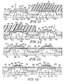
- FIG. 2 A portion of the reverse masking step is illustrated in Figure 2 after the implant using the first mask and the application of the thin second mask layer prior to the removal of the first mask layer and the superimposed second mask material.
- This method also includes a planarization process by which planarization material is applied and the resulting structure is removed before selectively removing the first mask.
- Another object of the present invention is to provide a reverse image masking technique which allows the formation of truly self-aligned twin wells.
- Still another object of the present invention is to provide a single photolithographic step, reverse masking technique which produces self-aligned twin wells.
- Yet another object of the present invention is to minimize latch-up.
- a further object of the present invention is to provide a process which allows tailoring of the threshold of the devices.
- An even further object of the present invention is to inhibit hot electron and substrate current injection.
- a still even further object of the present invention is to provide a reduced resistance of junction in contacts.
- Another object of the present invention is to lower the overall capacitance of the integrated circuit.
- a gate insulative layer and gate materials are formed on two well areas. This is followed by forming shallow source and drain regions using the gate as a mask in each of the wells.
- insulative spacers are formed extending laterally from the first and second gates over the source and drain regions and impurities are introduced to form deeper source and drain regions using the gate and the spacers as a mask. This is followed by the forming of the contacts to the respective layers.
- the gate material is polycrystalline silicon and the impurity introduction steps are carried out by ion implantation.
- a metal silicide step is performed to reduce the contact resistance by forming metal silicide over the source and drain regions as well as the gate. Insulative inserts are formed between the device regions by etching and filling by deposition to form planar oxide inserts separating the device regions laterally.
- the removal of the third mask material to reveal the second mask material may be achieved by removing the third mask layer to reveal at least the edges of the openings in the second mask layer. This reduces the amount of removal processing.
- the three mask layers must be of materials with sufficiently different characteristics such that they may be selectively removed.
- the three mask layers may be selected from positive and negative photosensitive resist materials or photoresist materials and a metallic material.
- photosensitive resist material two types are used, one mask is formed using a positive photosensitive resist wherein the mask layer is the unexposed portion after developing. After the introduction of impurities, and before the application of the next mask material, the remaining photoresist mask layer is radiation treated to form a hardened mask layer. The next mask layer, after being applied, is removed to reveal at least portions of the hardened mask material which is then selectively removed with any superimposed portion of the next mask layer thereon. This forms the inverse mask.
- the next mask material may either be a positive or negative photoresist mask since the radiation treated and hardened portion of the first photoresist mask can be selectively removed even with the same photosensitive resist material used in the second photoresist layer. If it is negative photosensitive resist, radiation treatment may not be necessary.
- a method of forming the inverse mask is illustrated in Figures 3 to 8.
- the first mask material will be a metal mask for example, aluminium
- the second mask material will be the photoresist mask.
- the technique is used on a substrate having no lateral dielectric isolation.
- the process begins by forming a first masking layer for example, a metal layer (40), on the top surface of the substrate (20) and separated therefrom by thin oxide layer (32).
- a thin photoresist material (46) having a thickness in the range of 0.5-1.5 ⁇ m (5,000 to 15,000 Angstroms) is then applied to the metal (40) and exposed to a desired pattern to form exposed regions (46') and unexposed regions (46).
- the structure is illustrated in Figure 3.
- the exposed portions (46') are then removed by a positive developer.
- the process so far has been described for a positive photoresist wherein the exposed portions are removed.
- the unexposed photoresist layer (46) is then used as a mask for the removal by etching of the metal layer (40). This etching may be performed by wet or dry etching as well as reactive ion etching. If a wet etch is used, the resultant side walls should be vertical to preserve the self-aligning effect.
- the resulting structure as illustrated in Figure 4 is a two-layer mask having photoresist portion (46) and metal portion (40). P type impurities for example, boron are introduced using the first mask layer as an alignment mask to form the P-wells (38).
- the photoresist layer (46) Prior to the application of the second masking level, the photoresist layer (46) is exposed to for example, deep ultraviolet light to form a hard exposed photoresist. Depending upon the specific second mask material, the hardening step may not be necessary to prevent intermixing of the photoresists. This exposure may take place any time after the selective removal of the previous exposed portions (46') of Figure 3 and the application of the second mask layer.
- the second mask layer (34) is applied as illustrated in Figure 5.
- a second mask layer may be a negative photoresist material.
- the second photoresist material is applied to a sufficient thickness so as to at least fill the openings (36) in the first mask level. This height should be at least to the height of the first mask level (40) and preferably to the combination of the height of the first mask level (40) and the photoresist level (46').
- the second mask level (34) is removed until the edges (48) of the photoresist layer (46') are revealed as illustrated in Figure 6.
- the photoresist layer (46') is then selectively removed using an appropriate wet or dry etchant and the superimposed portion of the second photoresist layer (34) is also removed.
- the resulting structure is illustrated in Figure 7 wherein the first mask level (40) is surrounded laterally by the second mask level (34).
- the first mask level (40) may be selectively removed resulting in the mask of Figure 8.
- N type impurities for example, phosphorus are introduced to form the N- well region (41).
- Figures 3 to 8 use a positive photoresist as a first masking layer and a negative photoresist as the second masking layer. This is the preferred embodiment since the positive photoresist, having an exposed pattern more easily removed than the unexposed pattern, allows for a subsequent exposure step prior to the formation of the second mask. This exposure step will prevent and reduce intermixing of the positive and negative photoresist to assure a true inverse masking operation. Depending upon the photoresist material used, the exposure hardening step may be deleted.
- the photoresist material forming the second mask is never exposed so as to change character since it is used as an impurity introduction mask patterned by a lift-off style technique.
- a single photoresist material may be used for both the first and second mask.
- the first mask (46) may be a positive photoresist wherein the exposed portions are removed by developer and followed by ion implantation. The unexposed portion is then exposed and new positive photoresist material may be applied to form the region (34). Since the first mask region (46') is an exposed photoresist, it has different characteristics than the unexposed second positive photoresist layer (34) and, thus, they can be selectively removed by developer.
- the present process may be performed with any combination of photoresist as long as they have sufficiently different characteristics such that the first mask can be selectively removed with the overlying second mask.
- Complementary insulated gate field effect transistors are formed by forming a gate oxide layer (49) on the surface of the substrate by, for example, exposing the substrate to an oxidizing atmosphere followed by the application of a gate material and delineation to form gate regions (50) and (52).
- the gates (50) and (52) are made from polycrystalline silicon.
- a first type P impurity for example boron, is ion implanted non-selectively using the gates (50) and (52) and the oxide inserts (30) as a mask to produce shallow regions (56) in well (38) and shallow regions (54) in well (41) as illustrated in Figure 9.
- a mask is formed by applying photoresist layer (58) and delineating to mask the N- well region (41) and expose the P-well region (38).
- N-type impurities for example arsenic, are implanted using the mask (58) and the gate (50) in combination with oxide inserts (30) to form shallow N+ source and drain regions (60).
- the ion implantation is carried out at a sufficient level to overcome the original P+ regions (56) in well (38).
- the initial introduction of P+ impurities into the P- well (38) allows for greater range for the formation of the N+ source and drain regions (60).
- the resulting structure is illustrated in Figure 10.
- the mask layer (58) is removed.
- the structure at this point has shallow source and drain regions formed in each of the complementary field effect transistor wells having a depth in the range of 100-200 nm (1000 to 2000 Angstroms) and an impurity concentration in the range of 1018 to 1019 atoms per cubic centimeter.
- the next sequence of operation form the deep source and drain region portions.
- This process begins with the formation of spacers extending laterally from the gate regions (50) and (52). These spacers are formed by depositing an insulative layer, for example chemical vapor deposition of silicon dioxide over the surface of the substrate. The oxide layer is then reactive ion etched to form the spacer regions (62) extending from gate (50) and spacers (64) extending from gate (52). These spacers result from the uneven topology of the deposited silicon oxide layer. This process is well known in the prior art and, thus, is not described in detail.
- a masking layer (66) is applied over the substrate and delineated to mask N- well region (41) and expose P- well region (38).
- N+ impurities for example phosphorus, are ion implanted using the mask layer (66), the gate (50) and the spacers (62) as well as inserts (30) as a mask. This results in deep N+ source and drain regions (68) extending laterally from the shallow N+ source and drain regions (60) as illustrated in Figure 11.
- the masking layer (66) is removed and a new masking layer (70) is applied and delineated to expose well (41) and mask well (38).
- P-type impurities for example boron
- the photoresist layer (70) is removed. This completes the device formation steps.
- the polycrystalline gates (50) and (52) are of a lower resistance and are doped as N+ and P+ respectively having an impurity concentration in the range of 1018 to 1020 atoms per cubic centimeter.
- a silicide forming metal layer (74) is applied to the substrate as illustrated in Figure 13.
- This layer may be, for example platinum.
- the wafer is then heated to cause platinum silicide to form in those regions where the platinum contacts the polycrystalline silicon gate or the silicon substrate. As illustrated in Figure 14, this includes the platinum silicide regions (76) on deep source and drain regions (68), region (78) on gate (50), regions (80) on deep source and drain regions (72) and region (82) on gate (52).
- No platinum silicide is formed over the oxide inserts (30) or the spacers (62) and (64). The portions of the platinum which should not form platinum silicide is easily selectively removed using for example hot concentrated Aqua Regia.
- oxide spacers inhibit hot electron and substrate current injection as well as providing better gate oxide reliability. Used in combination with the metal forming silicides, a self-alignment technique for the silicide formation without a mask results.
- the spacers also smooth out the sharp edges of the gate material for better contact metal coverage.
- a field oxide layer (84) is then formed over the wafer by chemical vapor deposition for example and vias are etched to provide contacts to the platinum silicide portion of the source and drain regions and the gate regions.
- a layer of contact metal is then applied and delineated to form contacts (86).
- the resulting structure is illustrated in Figure 15.
- An insulative layer may be provided over the first metal layer (86) and a second layer of metal provided.
- An alternative method for forming the shallow and deep source and drain regions includes, as illustrated in Figure 16, forming the masking layer (58) blocking the N- well region (41) and exposing the P-well region (38).
- the N+ arsenic implant is performed to form shallow source and drain regions (60).
- the photoresist layer (58) is removed and a photoresist layer (88) is applied and delineated to form a mask layer blocking the P-well region (38) and exposing the N- well region (41).
- P+ type impurities are implanted to form the P+ source and drain regions (54) as illustrated in Figure 17.
- the masking layer (88) is removed and a non-selective p-type boron implant is performed forming deep P+ source and drain regions (72) and P+ source and drain regions (90) in wells (41) and (38) respectively as illustrated in Figure 18.
- a masking layer (66) is applied and delineated to expose the P- well region (38) and block the N- well region (41).
- N-type impurities for example phosphorus, are implanted to form the deep N+ source and drain regions (68). This implantation must be carried out at sufficient power levels to overcome the P+ regions (90) originally formed in the prior step.
- the resulting structure is illustrated in Figure 19.
- the mask layer (66) is removed and the process is continued as previously described for Figures 13 to 15.
- the process of Figures 16 to 19 is substantially similar to the process steps of Figures 9 to 12 in that three masking steps are used for four implantations to form the two part source and drain regions for complementary insulated gate field effect transistors. This results since one of the implantation or doping step is performed non-selectively. The difference is, in Figures 9 to 12, the non-selective implantation is at the beginning of the process, whereas in the process of Figures 16 to 19, the non-selective implantation is in the middle of the process. As can be noted, the implantation of the P and N source and drain regions have been reversed in the two process flows. Since all the impurity introduction is by low temperature ion implantation, it is not critical that the N implantation precede the P implantation. The importance of the sequence of steps is that the shallow source and drain regions are formed using the gate as the alignment mask and that the deeper regions are formed using the spacer as the alignment mask.
Landscapes
- Engineering & Computer Science (AREA)
- Physics & Mathematics (AREA)
- Condensed Matter Physics & Semiconductors (AREA)
- General Physics & Mathematics (AREA)
- Manufacturing & Machinery (AREA)
- Computer Hardware Design (AREA)
- Microelectronics & Electronic Packaging (AREA)
- Power Engineering (AREA)
- Chemical & Material Sciences (AREA)
- Inorganic Chemistry (AREA)
- Metal-Oxide And Bipolar Metal-Oxide Semiconductor Integrated Circuits (AREA)
Claims (10)
- Verfahren zum Herstellen selbstjustierter Bereiche in einem Substrat (20), bei dem
eine erste Maskenschicht (40) eines ersten Materials auf das Substrat (20) aufgebracht wird,
eine zweite, zumindest eine Öffnung enthaltende Maskenschicht (46) eines zweiten Materials auf die erste Maskenschicht (40) aufgebracht wird,
ein Teil der ersten Maskenschicht (40) in der Öffnung der zweiten Maskenschicht entfernt und damit durch Ausbildung einer das Substrat freilegenden Öffnung (36) eine erste Maske hergestellt wird,
Verunreinigungen eines ersten Leitfähigkeitstyps durch die Öffnung (36) in der ersten und der zweiten Maskenschicht in das Substrat (20) eingebracht werden, zur Ausbildung eines ersten Senken-Bereichs (38),
eine dritte Maskenschicht (34) eines dritten Materials so aufgebracht wird, daß zumindest die Öffnung (36) in der ersten Maske ausgefüllt wird,
die dritte Maskenschicht (34) entfernt wird, bis ein Teil der zweiten Maskenschicht (46') freiliegt,
die zweite Maskenschicht (46') mit einer eventuell darüberliegenden dritten Schicht (34) selektiv entfernt und dadurch die erste Maskenschicht (40) freigelegt wird,
die erste Maskenschicht (40) selektiv entfernt und dadurch eine zweite Maske als Kehrbild der ersten Maske ausgebildet wird und
Verunreinigungen eines zweiten Leitfähigkeitstyps durch Öffnungen in der zweiten Maske in das Substrat (20) eingebracht werden, zur Ausbildung zweiter, mit den ersten Senken-Bereichen (38) ausgerichteter Senken-Bereiche (41). - Verfahren nach Anspruch 1, bei dem die zweiten und dritten Materialen (46, 34) unterschiedliche photoempfindliche Lacke sind.
- Verfahren nach Anspruch 1 oder 2, bei dem das erste Material (40) ein metallisches Material und das zweite Material (46) ein photoempfindlicher Lack ist.
- Verfahren nach Anspruch 1 oder 2, bei dem die zweite Maskenschicht (46) mit einer Stärke im Bereich von 500 bis 1500 nm aufgebracht wird.
- Verfahren nach Anspruch 1 oder 4, bei dem die dritte Maskenschicht (34) mit einer Stärke mindestens gleich der Stärke der ersten Maskenschicht (40) aufgebracht wird.
- Verfahren nach Anspruch 1, bei dem das zweite Material (46) ein positiver photoempfindlicher Lack ist und die zweite Maskenschicht (46) nach Ausbildung der Öffnung (36) in der ersten Maskenschicht (40) und vor dem Aufbringen der dritten Maskenschicht (34) belichtet wird.
- Verfahren nach Anspruch 1, das die Ausbildung von Isolierschicht-Feldeffekttransistoren beinhaltet und bei dem ferner
eine Gatter-Isolierschicht (49) auf dem Substrat ausgebildet wird, erste und zweite Gatter (50, 52) auf der Gatter-Isolierschicht (49) jeweils über der ersten und der zweiten Senke (38, 41) ausgebildet werden,
Verunreinigungen eines zweiten Leitfähigkeitstyps mit Hilfe des ersten Gatters (50) als Maske in die erste Senke (38) eingeführt und damit flache Quellen- und Senkenbereiche (60) ausgebildet werden,
Verunreinigungen eines ersten Leitfähigkeitstyps mit Hilfe des zweiten Gatters (52) als Maske in die zweite Senke (41) eingeführt und damit flache Quellen- und Senkenbereiche (54) ausgebildet werden,
isolierende Abstandsschichten (62, 64) seitlich der ersten und zweiten Gatter (50, 52) über den Quellen- und Senkenbereichen ausgebildet werden,
Verunreinigungen eines ersten Leitfähigkeitstyps mit Hilfe des zweiten Gatters (52) und der Abstandsschichten (64) als Maske in die zweite Senke (41) eingeführt werden zur Ausbildung tiefer Quellen- und Senkenbereiche (72), die eine größere Tiefe aufweisen als die flachen Quellen- und Senkenbereiche, und
Verunreinigungen eines zweiten Leitfähigkeitstyps mit Hilfe des ersten Gatters (50) und der Abstandsschichten (62) als Maske in die erste Senke (38) eingeführt werden zur Ausbildung tiefer Quellen- und Senkenbereiche (68), die eine größere Tiefe aufweisen als die flachen Quellen- und Senkenbereiche. - Verfahren nach Anspruch 7, bei dem die ersten und zweiten Gatter (50, 52) und das Substrat aus Silizium bestehen und bei dem ferner vor Ausbildung der Quellen- und Senkenbereiche Oxidbereiche (30) zwischen den Senken (38, 41) ausgebildet werden,
nach der Ausbildung der tiefen Quellen- und Senkenbereiche über dem Substrat in nicht selektiver Weise ein silicidbildendes Material (74) aufgebracht wird,
durch Erhitzen ein Metall-Silicid (76, 78, 80, 82) auf den Gattern und Quellen- und Senkenbereichen ausgebildet wird und
das silicidbildende Material von den Abstandsschichten (62, 64) und den Oxidbereichen (30) entfernt wird. - Verfahren nach Anspruch 7, bei dem
das Einbringen der Verunreinigungen zur Ausbildung der flachen Quellen- und Senkenbereiche (54) in der zweiten Senke (41) nur mittels der Gatter (50, 52) als Maske erfolgt,
das Einbringen von Verunreinigungen zur Ausbildung der flachen Quellen- und Senkenbereiche (60) in der ersten Senke (38) den Schritt umfaßt, eine die zweite Senke (41) abdeckende Maske (58) auszubilden,
das Einbringen von Verunreinigungen zur Ausbildung der tiefen Quellen- und Senkenbereiche (72) in der zweiten Senke (41) den Schritt umfaßt, eine die erste Senke (38) abdeckende Maske (70) auszubilden, und
das Einbringen von Verunreinigungen zur Ausbildung der tiefen Quellen- und Senkenbereiche (68) in der ersten Senke (38) den Schritt umfaßt, eine die zweite Senke (41) abdeckende Maske (66) auszubilden. - Verfahren nach Anspruch 7, bei dem
das Einbringen von Verunreinigungen zur Ausbildung der flachen Quellen- und Senkenbereiche (60) in der ersten Senke (38) den Schritt umfaßt, eine die zweite Senke (41) abdeckende Maske (58) auszubilden,
das Einbringen der Verunreinigungen zur Ausbildung der flachen Quellen- und Senkenbereiche (54) in der zweiten Senke (41) den Schritt umfaßt, eine die erste Senke (38) abdeckende Maske (88) auszubilden,
das Einbringen von Verunreinigungen zur Ausbildung der tiefen Quellen- und Senkenbereiche (72) in der zweiten Senke (41) nur mittels des Gatters (52) als Maske erfolgt und
das Einbringen von Verunreinigungen zur Ausbildung der tiefen Quellen- und Senkenbereiche (68) in der ersten Senke (38) den Schritt umfaßt, eine die zweite Senke (41) abdeckende Maske (66) auszubilden.
Applications Claiming Priority (4)
| Application Number | Priority Date | Filing Date | Title |
|---|---|---|---|
| US06/620,835 US4599789A (en) | 1984-06-15 | 1984-06-15 | Process of making twin well VLSI CMOS |
| US643362 | 1984-08-22 | ||
| US620835 | 1984-08-22 | ||
| US06/643,362 US4578859A (en) | 1984-08-22 | 1984-08-22 | Implant mask reversal process |
Publications (3)
| Publication Number | Publication Date |
|---|---|
| EP0164737A2 EP0164737A2 (de) | 1985-12-18 |
| EP0164737A3 EP0164737A3 (en) | 1987-05-13 |
| EP0164737B1 true EP0164737B1 (de) | 1991-09-18 |
Family
ID=27088796
Family Applications (1)
| Application Number | Title | Priority Date | Filing Date |
|---|---|---|---|
| EP19850107216 Expired EP0164737B1 (de) | 1984-06-15 | 1985-06-12 | Verfahren zum Herstellen selbstjustierter Bereiche in einem Substrat |
Country Status (3)
| Country | Link |
|---|---|
| EP (1) | EP0164737B1 (de) |
| JP (1) | JPH0669079B2 (de) |
| DE (1) | DE3584113D1 (de) |
Cited By (1)
| Publication number | Priority date | Publication date | Assignee | Title |
|---|---|---|---|---|
| CN104810253A (zh) * | 2014-01-28 | 2015-07-29 | 中芯国际集成电路制造(上海)有限公司 | 半导体器件的形成方法 |
Families Citing this family (7)
| Publication number | Priority date | Publication date | Assignee | Title |
|---|---|---|---|---|
| US4767721A (en) * | 1986-02-10 | 1988-08-30 | Hughes Aircraft Company | Double layer photoresist process for well self-align and ion implantation masking |
| FR2610141B1 (fr) * | 1987-01-26 | 1990-01-19 | Commissariat Energie Atomique | Circuit integre cmos et procede de fabrication de zones d'isolation electrique dans ce circuit |
| JPS63196070A (ja) * | 1987-02-10 | 1988-08-15 | Sony Corp | Cmosの製造方法 |
| IT1225614B (it) * | 1988-08-04 | 1990-11-22 | Sgs Thomson Microelectronics | Processo per la fabbricazione di dispositivi integrati cmos con lunghezze di gate ridotte e drain leggermente drogato |
| JPH088307B2 (ja) * | 1988-12-20 | 1996-01-29 | 株式会社東芝 | 半導体装置の製造方法 |
| US4895520A (en) * | 1989-02-02 | 1990-01-23 | Standard Microsystems Corporation | Method of fabricating a submicron silicon gate MOSFETg21 which has a self-aligned threshold implant |
| JP2007251194A (ja) * | 2007-05-14 | 2007-09-27 | Toshiba Corp | 半導体装置およびその製造方法 |
Family Cites Families (3)
| Publication number | Priority date | Publication date | Assignee | Title |
|---|---|---|---|---|
| DE3175081D1 (en) * | 1980-12-12 | 1986-09-11 | Toshiba Kk | Method of manufacturing a semiconductor device of the mis type |
| US4411058A (en) * | 1981-08-31 | 1983-10-25 | Hughes Aircraft Company | Process for fabricating CMOS devices with self-aligned channel stops |
| US4435896A (en) * | 1981-12-07 | 1984-03-13 | Bell Telephone Laboratories, Incorporated | Method for fabricating complementary field effect transistor devices |
-
1985
- 1985-06-12 DE DE8585107216T patent/DE3584113D1/de not_active Expired - Lifetime
- 1985-06-12 EP EP19850107216 patent/EP0164737B1/de not_active Expired
- 1985-06-15 JP JP60130674A patent/JPH0669079B2/ja not_active Expired - Lifetime
Cited By (1)
| Publication number | Priority date | Publication date | Assignee | Title |
|---|---|---|---|---|
| CN104810253A (zh) * | 2014-01-28 | 2015-07-29 | 中芯国际集成电路制造(上海)有限公司 | 半导体器件的形成方法 |
Also Published As
| Publication number | Publication date |
|---|---|
| EP0164737A2 (de) | 1985-12-18 |
| DE3584113D1 (de) | 1991-10-24 |
| EP0164737A3 (en) | 1987-05-13 |
| JPS6158265A (ja) | 1986-03-25 |
| JPH0669079B2 (ja) | 1994-08-31 |
Similar Documents
| Publication | Publication Date | Title |
|---|---|---|
| US4599789A (en) | Process of making twin well VLSI CMOS | |
| EP0127725B1 (de) | Verfahren zum Herstellen einer Halbleiteranordnung mit schwach dotierten Gebieten | |
| US4788160A (en) | Process for formation of shallow silicided junctions | |
| US6875697B2 (en) | Dual depth trench isolation | |
| US4824796A (en) | Process for manufacturing semiconductor BICMOS device | |
| US4752589A (en) | Process for the production of bipolar transistors and complementary MOS transistors on a common silicon substrate | |
| EP0179810B1 (de) | Technologie der integrierten cmos-schaltung | |
| JPS6196759A (ja) | 集積回路の形成方法 | |
| US4992388A (en) | Short channel IGFET process | |
| EP0136632B1 (de) | Verfahren zum Implantieren von selbstausrichtenden Source- und Draingebieten mit Hilfe einer einzigen Maske, zum Herstellen einer CMOS-Struktur | |
| US4906585A (en) | Method for manufacturing wells for CMOS transistor circuits separated by insulating trenches | |
| US5904529A (en) | Method of making an asymmetrical IGFET and providing a field dielectric between active regions of a semiconductor substrate | |
| GB2100926A (en) | Field effect transistors | |
| US4866001A (en) | Very large scale bipolar integrated circuit process | |
| US4578859A (en) | Implant mask reversal process | |
| US4075754A (en) | Self aligned gate for di-CMOS | |
| EP0164737B1 (de) | Verfahren zum Herstellen selbstjustierter Bereiche in einem Substrat | |
| EP0459398B1 (de) | Herstellungsverfahren eines Kanals in MOS-Halbleiteranordnung | |
| EP0656645B1 (de) | Feldeffekttransistor mit einem versiegelten diffundierten Übergang | |
| US5547903A (en) | Method of elimination of junction punchthrough leakage via buried sidewall isolation | |
| JPS58116775A (ja) | Mesfet装置の製造方法及びその装置 | |
| US5175127A (en) | Self-aligned interlayer contact process using a plasma etch of photoresist | |
| US6171914B1 (en) | Synchronized implant process to simplify NLDD/PLDD stage and N+/P+stage into one implant | |
| JPH05102403A (ja) | 半導体装置の製造方法 | |
| JP3092854B2 (ja) | 半導体デバイス用のセルフアラインメント技術 |
Legal Events
| Date | Code | Title | Description |
|---|---|---|---|
| PUAI | Public reference made under article 153(3) epc to a published international application that has entered the european phase |
Free format text: ORIGINAL CODE: 0009012 |
|
| AK | Designated contracting states |
Designated state(s): DE FR GB IT NL |
|
| PUAL | Search report despatched |
Free format text: ORIGINAL CODE: 0009013 |
|
| AK | Designated contracting states |
Kind code of ref document: A3 Designated state(s): DE FR GB IT NL |
|
| 17P | Request for examination filed |
Effective date: 19870901 |
|
| 17Q | First examination report despatched |
Effective date: 19890710 |
|
| ITF | It: translation for a ep patent filed | ||
| GRAA | (expected) grant |
Free format text: ORIGINAL CODE: 0009210 |
|
| AK | Designated contracting states |
Kind code of ref document: B1 Designated state(s): DE FR GB IT NL |
|
| REF | Corresponds to: |
Ref document number: 3584113 Country of ref document: DE Date of ref document: 19911024 |
|
| ET | Fr: translation filed | ||
| PLBE | No opposition filed within time limit |
Free format text: ORIGINAL CODE: 0009261 |
|
| STAA | Information on the status of an ep patent application or granted ep patent |
Free format text: STATUS: NO OPPOSITION FILED WITHIN TIME LIMIT |
|
| 26N | No opposition filed | ||
| REG | Reference to a national code |
Ref country code: GB Ref legal event code: IF02 |
|
| PGFP | Annual fee paid to national office [announced via postgrant information from national office to epo] |
Ref country code: NL Payment date: 20040517 Year of fee payment: 20 |
|
| PGFP | Annual fee paid to national office [announced via postgrant information from national office to epo] |
Ref country code: GB Payment date: 20040609 Year of fee payment: 20 |
|
| PGFP | Annual fee paid to national office [announced via postgrant information from national office to epo] |
Ref country code: FR Payment date: 20040618 Year of fee payment: 20 |
|
| PGFP | Annual fee paid to national office [announced via postgrant information from national office to epo] |
Ref country code: DE Payment date: 20040802 Year of fee payment: 20 |
|
| PG25 | Lapsed in a contracting state [announced via postgrant information from national office to epo] |
Ref country code: GB Free format text: LAPSE BECAUSE OF EXPIRATION OF PROTECTION Effective date: 20050611 |
|
| PG25 | Lapsed in a contracting state [announced via postgrant information from national office to epo] |
Ref country code: NL Free format text: LAPSE BECAUSE OF EXPIRATION OF PROTECTION Effective date: 20050612 |
|
| REG | Reference to a national code |
Ref country code: GB Ref legal event code: PE20 |
|
| NLV7 | Nl: ceased due to reaching the maximum lifetime of a patent |
Effective date: 20050612 |