EP0152600B1 - Vorrichtung und Verfahren zur Behandlung von Leiterplatten - Google Patents
Vorrichtung und Verfahren zur Behandlung von Leiterplatten Download PDFInfo
- Publication number
- EP0152600B1 EP0152600B1 EP84115512A EP84115512A EP0152600B1 EP 0152600 B1 EP0152600 B1 EP 0152600B1 EP 84115512 A EP84115512 A EP 84115512A EP 84115512 A EP84115512 A EP 84115512A EP 0152600 B1 EP0152600 B1 EP 0152600B1
- Authority
- EP
- European Patent Office
- Prior art keywords
- circuit boards
- treatment
- printed circuit
- solutions
- solution
- Prior art date
- Legal status (The legal status is an assumption and is not a legal conclusion. Google has not performed a legal analysis and makes no representation as to the accuracy of the status listed.)
- Expired - Lifetime
Links
- 238000000034 method Methods 0.000 title claims description 22
- 238000011282 treatment Methods 0.000 title claims description 17
- 230000008569 process Effects 0.000 claims description 11
- 238000010924 continuous production Methods 0.000 claims 1
- 239000012756 surface treatment agent Substances 0.000 claims 1
- 239000000243 solution Substances 0.000 description 33
- 239000012487 rinsing solution Substances 0.000 description 9
- XLYOFNOQVPJJNP-UHFFFAOYSA-N water Chemical compound O XLYOFNOQVPJJNP-UHFFFAOYSA-N 0.000 description 8
- KDLHZDBZIXYQEI-UHFFFAOYSA-N Palladium Chemical compound [Pd] KDLHZDBZIXYQEI-UHFFFAOYSA-N 0.000 description 4
- QAOWNCQODCNURD-UHFFFAOYSA-N Sulfuric acid Chemical compound OS(O)(=O)=O QAOWNCQODCNURD-UHFFFAOYSA-N 0.000 description 4
- WSFSSNUMVMOOMR-UHFFFAOYSA-N Formaldehyde Chemical compound O=C WSFSSNUMVMOOMR-UHFFFAOYSA-N 0.000 description 3
- MHAJPDPJQMAIIY-UHFFFAOYSA-N Hydrogen peroxide Chemical compound OO MHAJPDPJQMAIIY-UHFFFAOYSA-N 0.000 description 3
- 230000004913 activation Effects 0.000 description 3
- 150000008044 alkali metal hydroxides Chemical class 0.000 description 3
- 238000007747 plating Methods 0.000 description 3
- 239000000126 substance Substances 0.000 description 3
- RYGMFSIKBFXOCR-UHFFFAOYSA-N Copper Chemical compound [Cu] RYGMFSIKBFXOCR-UHFFFAOYSA-N 0.000 description 2
- 229910001854 alkali hydroxide Inorganic materials 0.000 description 2
- 239000012670 alkaline solution Substances 0.000 description 2
- 239000002585 base Substances 0.000 description 2
- -1 cleaners Substances 0.000 description 2
- 229910052802 copper Inorganic materials 0.000 description 2
- 239000010949 copper Substances 0.000 description 2
- 238000005530 etching Methods 0.000 description 2
- 238000007654 immersion Methods 0.000 description 2
- 238000006386 neutralization reaction Methods 0.000 description 2
- 229910052763 palladium Inorganic materials 0.000 description 2
- 230000009467 reduction Effects 0.000 description 2
- 239000007921 spray Substances 0.000 description 2
- KCXVZYZYPLLWCC-UHFFFAOYSA-N EDTA Chemical compound OC(=O)CN(CC(O)=O)CCN(CC(O)=O)CC(O)=O KCXVZYZYPLLWCC-UHFFFAOYSA-N 0.000 description 1
- 230000009471 action Effects 0.000 description 1
- 229910052783 alkali metal Inorganic materials 0.000 description 1
- 150000003927 aminopyridines Chemical class 0.000 description 1
- 230000008901 benefit Effects 0.000 description 1
- 230000015572 biosynthetic process Effects 0.000 description 1
- 239000003795 chemical substances by application Substances 0.000 description 1
- 238000004140 cleaning Methods 0.000 description 1
- 238000010276 construction Methods 0.000 description 1
- 150000001879 copper Chemical class 0.000 description 1
- 230000001419 dependent effect Effects 0.000 description 1
- 239000003822 epoxy resin Substances 0.000 description 1
- 239000011521 glass Substances 0.000 description 1
- 230000005484 gravity Effects 0.000 description 1
- 239000000463 material Substances 0.000 description 1
- 239000000203 mixture Substances 0.000 description 1
- 150000002940 palladium Chemical class 0.000 description 1
- 229920000647 polyepoxide Polymers 0.000 description 1
- 238000005507 spraying Methods 0.000 description 1
- 239000000080 wetting agent Substances 0.000 description 1
Images


Classifications
-
- H—ELECTRICITY
- H05—ELECTRIC TECHNIQUES NOT OTHERWISE PROVIDED FOR
- H05K—PRINTED CIRCUITS; CASINGS OR CONSTRUCTIONAL DETAILS OF ELECTRIC APPARATUS; MANUFACTURE OF ASSEMBLAGES OF ELECTRICAL COMPONENTS
- H05K3/00—Apparatus or processes for manufacturing printed circuits
- H05K3/0085—Apparatus for treatments of printed circuits with liquids not provided for in groups H05K3/02 - H05K3/46; conveyors and holding means therefor
Definitions
- the invention relates to a device for treating printed circuit boards according to the preamble of claim 1.
- base material which may be copper-clad
- suitable process solutions such as cleaners, rinsing solutions, etching solutions, neutralization solutions, activation solutions, reduction solutions, chemical baths and others, and to contact them perfectly with drilled plates.
- This treatment is carried out on the one hand by immersion treatment, in that the plates suspended on racks are dipped into the containers filled with the respective treatment solutions by means of transport devices and transported from container to container, which requires a large space for the entire treatment system.
- the through-contacting of printed circuit boards according to this technique is usually unsatisfactory and time-consuming.
- the spray treatment by spraying the printed circuit boards is primarily used for rinsing and is not suitable for aggressive process solutions, since the solutions are atomized at the required spray pressure and therefore cannot be sufficiently effective on the boards. Vias are also unsatisfactory when using this technique.
- a device according to the preamble of claim 1 is known from US-A-7371722.
- the object of the present invention is to provide a device and a method which enable space and time-saving treatment of vertically conveyed printed circuit boards with process solutions up to through-plating.
- the device according to the invention surprisingly enables extremely space-saving, process-dependent treatment of printed circuit boards up to through-plating.
- the process solutions are applied to the plates in such a way that they pour out gushingly over their surface and flow downward due to the force of gravity, with strongly turbulent flows forming in the boreholes.
- the turbulence caused thereby prevents the formation of air bubbles and ensures intensive contact of the process solutions with the hole surface, which is hereby treated in the desired sense in previously unknown dimensions.
- a particularly suitable process solution for activation is, for example, an aqueous alkaline solution of a palladium complex, such as palladium salt in aminopyridine, which is swelled up with appropriately adapted pre- and post-treatment solutions.
- a palladium complex such as palladium salt in aminopyridine
- the printed circuits produced according to the invention therefore have excellent characteristics.
- the device according to the invention can be constructed in a lightweight construction, since the tubs and heavy transport devices which have been customary up to now are eliminated.
- the small space requirement of the device also makes it possible to isolate it from the environment without major technical effort and thus to operate it in an environmentally friendly manner.
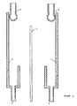
- FIG. 3 shows the function of the device according to the invention when treating the printed circuit board (side view).
- Figure 4 shows the function of the device according to the invention in idle (side view).
- Usual base plates made of double-sided copper-clad glass fiber-reinforced epoxy resin were drilled in the usual way and then hung in a continuous conveyor, which provided the plates by means of modularly connected devices according to the invention with separate feeds for different process solutions.
- the total time of the treatment was accordingly 5.5 minutes, after which the plates were chemically metallized in the usual manner using a conventional chemical copper bath containing a copper salt, ethylenediaminetetraacetic acid, alkali metal cyanide, alkali metal hydroxide and formaldehyde.
- the total time of the conventional treatment technique was consequently 25.5 minutes and was about 5 times as long as when the method according to the invention was carried out.
Landscapes
- Engineering & Computer Science (AREA)
- Manufacturing & Machinery (AREA)
- Microelectronics & Electronic Packaging (AREA)
- Manufacturing Of Printed Wiring (AREA)
- Chemically Coating (AREA)
- Electroplating Methods And Accessories (AREA)
- Printing Elements For Providing Electric Connections Between Printed Circuits (AREA)
Description
- Die Erfindung betrifft eine Vorrichtung zur Behandlung von Leiterplatten gemäß Oberbegriff des Anspruchs 1.
- Verfahren und Vorrichtung zur Behandlung von Leiterplatten sind bereits allgemein bekannt.
- Diese Behandlungen haben den Zweck, sogenanntes Basismaterial, das gegebenenfalls kupferkaschiert sein kann, durch Einwirkung von geeigneten Prozesslösungen, wie Reinigern, Spüllösungen, Ätzlösungen;Neutralisationslösungen, Aktivierungslösungen, Reduktionslösungen, chemischen Bädern und anderen mit Leiterbahnen zu versehen und diese bei gebohrten Platten einwandfrei durchzukontaktieren.
- Die Durchführung dieser Behandlung erfolgt einerseits durch Tauchbehandlung, indem die an Gestellen aufgehängten Platten mittels Transporteinrichtungen in die mit den jeweiligen Behandlungslösungen gefüllten Behälter getaucht und von Behälter zu Behälter transportiert werden, was einen großen Platzbedarf für die gesamte Behandlungsanlage voraussetzt. Die Durchkontaktierung von Leiterplatten nach dieser Technik ist in der Regel zudem unbefriedigend und zeitraubend.
- Die andererseits ausgeübte Spritzbehandlung durch Abspritzen der Leiterplatten wird vornehmlich zum Spülen angewendet und ist für aggressive Prozesslösungen nicht geeignet, da die Lösungen bei dem erforderlichen Spritzdruck vernebelt und daher auf den Platten gar nicht genügend wirksam werden können. Durchkontaktierungen sind bei Anwendung dieser Technik ebenfalls nicht befriedigend möglich. Eine Vorrichtung gemäβ Oberbegriff des Anspruches 1 ist aus US-A-7371722 bekannt.
- Aufgabe der vorliegenden Erfindung ist die Schaffung einer Vorrichtung und eines Verfahrens, die eine raum- und zeitsparende Behandlung von vertikal beförderten Leiterplatten mit Prozesslösungen bis zur Durchkontaktierung ermöglichen.
- Diese Aufgabe wird erfindungsgemäß durch den im Anspruch 1 gekennzeichneten Gegenstand gelöst.
- Die erfindungsgemäße Vorrichtung ermöglicht überraschenderweise eine extrem raumsparende prozessabhängige Behandlung von Leiterplatten bis zur Durchkontaktierung.
- Bei Durchführung des erfindungsgemäßen Verfahrens werden vorteilhafterweise bei erheblich kürzerer Behandlungszeit als nach bekannten Verfahren Leiterplatten mit hervorragender Durchkontaktierung hergestellt.
- Mittels der erfindungsgemäßen Vorrichtung werden die Prozesslösungen derart auf die Platten beaufschlagt, daß sie sich schwallartig über deren Oberfläche ergießen und infolge der Schwerkraft nach unten abfließen, wobei sich in den Bohrlöchern stark turbulente Strömungen ausbilden. Die hierdurch bewirkte Turbulenz verhindert das Entstehen von Luftblasen und sorgt für einen intensiven Kontakt der Prozesslösungen mit der Lochoberfläche, die hierdurch in bisher nicht bekannten Maße im gewünschten Sinne behandelt wird.
- Als besonders geeignete Prozesslösung zur Aktivierung sei beispielsweise eine wäßrige alkalische Lösung eines Palladiumkomplexes, wie Palladiumsalz in Aminopyridin, genannt, die mit entsprechend angepassten Vor- und Folgebehandlungslösungen aufgeschwallt wird.
- Die erfindungsgemäß hergestellten gedruckten Schaltungen weisen daher hervorragende Kenndaten auf.
- Von besonderem Vorteil ist es weiterhin, daß die erfindungsgemäße Vorrichtung in Leichtbauweise erstellt werden kann, da die bisher üblichen Wannen und schweren Transporteinrichtungen entfallen.
- Der geringe Platzbedarf der Vorrichtung ermöglicht es weiter-hin, diese ohne größeren technischen Aufwand von der Umgebung abzukapseln und damit umweltfreundlich zu betreiben.
- Da die Prozesslösungen im Kreislauf gefahren werden können, ist eine Filtration dieser Lösung problemlos möglich. Die Volumina dieser Lösungen können außerdem im Vergleich zu den bekannten Techniken erheblich verringert werden.
- Die Figuren dienen zur Erläuterung der Erfindung.
- Figur 1 zeigt die erfindungsgemäße Vorrichtung in Seitenansicht.
- Hierin bedeuten:
- 1 Auffanggefäß
2 Düsen
3 Leiterplatte an Stetigförderer
4 Ablauföffnungen
5 Sammelbehälter
6 verbindende Rohrleitungen mit Ventilen
7 verbindende Rohrleitungen mit Ventilen - Figur 2 zeigt einen Ausschnitt der erfindungsgemäßen Vorrichtung in Seitenansicht.
- Hierin bedeuten:
- 1 Auffanggefäß
2 Düsenkopf mit Querbohrungen
3 Leiterplatte
4 Ablauföffnungen - Figur 3 zeigt die Funktion der erfindungsgemäßen Vorrichtung beim Behandeln der Leiterplatte (Seitenansicht).
- Figur 4 zeigt die Funktion der erfindungsgemäßen Vorrichtung im Leerlauf (Seitenansicht).
- In Figuren 3 und 4 bedeuten:
- 1 Auffanggefäß
- 2 Düsen
- 3 Behandlungsmittel
- 4 Ablauföffnungen
- 5 Leiterplatte
- Das folgende Beispiel erläutert die Durchführung des Verfahrens.
- Übliche Basisplatten aus doppelseitig kupferkaschiertem glasfaserverstärktem Epoxidharz wurden in üblicher Weise gebohrt und dann in einen Stetigförderer eingehängt, der die Platten durch baukastenartig miteinander verbundene erfindungsgemäße Vorrichtungen versehen mit separaten Einspeisungen für unterschiedliche Prozesslösungen beförderte.
- Die folgenden Prozesslösungen üblicher Zusammensetzung wurden mit folgenden Behandlungszeiten auf die Platte beaufschlagt.
- 1. Reinigungslösung
- (auf Basis einer Alkalihydroxidlösung)
0,5 Minuten - 2. Spüllösung
- (wasser)
0,5 Minuten - 3. Ätzlösung
- (auf Basis einer stabilisierten schwefelsauren Lösung von Wasserstoffperoxid)
0,5 Minuten - 4. Spüllösung
- (Wasser)
0,5 Minuten - 5. Neutralisationslösung
- (auf Basis einer Alkalihydroxid-Lösung)
0,5 Minuten - 6. Spüllösung
- (Wasser)
1,0 Minuten - 7. Voraktivierungslösung
- (auf Basis einer netzmittelhaltigen Schwefelsäurelösung)
0,5 Minuten - 8. Aktivierungslösung
- (auf Basis einer alkalischen Lösung eines Palladiumkomplexes)
0,5 Minuten - 9. Spüllösung
- (Wasser)
0,5 Minuten - 10. Reduktionslösung
- (auf Basis einer Borhydrid-Lösung)
0,5 Minuten - Die Gesamtzeit der Behandlung betrug demzufolge 5,5 Minuten, wonach die Platten in üblicher Weise mittels eines üblichen chemischen Kupferbades enthaltend ein Kupfersalz, Äthylendiamintetraessigsäure, Alkalicyanid, Alkalihydroxid und Formaldehyd chemisch metallisiert wurden.
- Es entstanden in allen Fällen hervorragend durchkontaktierte Leiterplatten mit Kenndaten von mindestens 1.1012Ω.
- In analoger Weise wurden dann entsprechende Leiterplatten mittels üblicher Tauchverfahren behandelt, wofür folgende Behandlungszeiten erforderlich waren:

- Die Gesamtzeit der konventionellen Behandlungstechnik betrug demzufolge 25,5 Minuten und war um etwa 5 Mal so groß wie bei Durchführung des erfindungsgemäßen Verfahrens.
- Bei anschließender chemischer Verkupferung in analoger Weise wie oben angegeben wurden teilweise unbefriedigend durchkontaktierte Platten erhalten.
Claims (1)
- Vorrichtung zur Behandlung von vertikal orientierten Leiterplatten mit Prozesslösungen im vertikal kontinuierlichen, prozessabhängigen Durchlaufverfahren, mit Stetigförderer, Oberflächenbehandlungsmittel-Sammelbehälter und Düsen mit verbindenden Rohrleitungen, dadurch gekennzeichnet, daß sich oberhalb des Sammelbehälters zwei spiegelbildlich gleiche Auffanggefäße mit an ihrem unteren Ende angebrachten Ablauföfnungen befinden, die beidseitig parallel zur Förderrichtung der Leiterplatte angeordnet sind, wobei deren zur Leiterplatte gerichtete Wandseite kleiner als die äußere Wandseite ausgebildet ist.
Applications Claiming Priority (2)
| Application Number | Priority Date | Filing Date | Title |
|---|---|---|---|
| DE19843406583 DE3406583A1 (de) | 1984-02-21 | 1984-02-21 | Vorrichtung und verfahren zur behandlung von leiterplatten |
| DE3406583 | 1984-02-21 |
Publications (3)
| Publication Number | Publication Date |
|---|---|
| EP0152600A2 EP0152600A2 (de) | 1985-08-28 |
| EP0152600A3 EP0152600A3 (en) | 1987-04-22 |
| EP0152600B1 true EP0152600B1 (de) | 1991-02-20 |
Family
ID=6228627
Family Applications (1)
| Application Number | Title | Priority Date | Filing Date |
|---|---|---|---|
| EP84115512A Expired - Lifetime EP0152600B1 (de) | 1984-02-21 | 1984-12-15 | Vorrichtung und Verfahren zur Behandlung von Leiterplatten |
Country Status (6)
| Country | Link |
|---|---|
| US (1) | US4611554A (de) |
| EP (1) | EP0152600B1 (de) |
| JP (1) | JPS60198889A (de) |
| AT (1) | AT396311B (de) |
| CA (1) | CA1231595A (de) |
| DE (2) | DE3406583A1 (de) |
Families Citing this family (6)
| Publication number | Priority date | Publication date | Assignee | Title |
|---|---|---|---|---|
| DE3529313A1 (de) * | 1985-08-14 | 1987-02-26 | Schering Ag | Automatische transport- und behandlungseinrichtung fuer waren, insbesondere leiterplatten |
| US4862827A (en) * | 1988-06-28 | 1989-09-05 | Wacker-Chemie Gmbh | Apparatus for coating semiconductor components on a dielectric film |
| US5211756A (en) * | 1991-08-09 | 1993-05-18 | Micro-Plate/Systems | Apparatus to manufacture printed circuit boards |
| US5733376A (en) * | 1994-04-01 | 1998-03-31 | Argus International | Apparatus for spray coating opposing major surfaces of a workpiece |
| US5588996A (en) * | 1994-04-01 | 1996-12-31 | Argus International | Apparatus for spray coating flat surfaces |
| KR100399650B1 (ko) * | 2001-10-27 | 2003-09-29 | 삼성에스디아이 주식회사 | 리튬-황 전지용 양극 활물질 및 그의 제조 방법 |
Family Cites Families (9)
| Publication number | Priority date | Publication date | Assignee | Title |
|---|---|---|---|---|
| US3122449A (en) * | 1962-09-19 | 1964-02-25 | Motorola Inc | Method for metallizing non-conductors |
| US3298588A (en) * | 1964-01-23 | 1967-01-17 | Sanders Associates Inc | Printed circuit board and machine for soldering same |
| US3798050A (en) * | 1971-05-28 | 1974-03-19 | Ppg Industries Inc | Catalytic sensitization of substrates for metallization |
| US3931790A (en) * | 1971-07-06 | 1976-01-13 | Ppg Industries, Inc. | Angled crossfire rinses |
| JPS55156388A (en) * | 1979-05-24 | 1980-12-05 | Matsushita Electric Works Ltd | Method of forming electric path onto insulating substrate |
| SU913612A1 (ru) * | 1980-07-07 | 1982-03-15 | Igor N Kolokolov | Устройство для жидкостной обработки печатных плат, преимущественно для химического меднения 1 |
| US4371422A (en) * | 1980-10-15 | 1983-02-01 | Micro-Plate, Inc. | Continuous processing of printed circuit boards |
| US4454003A (en) * | 1983-01-06 | 1984-06-12 | Systems Engineering & Manufacturing Corp. | Printed circuit board component conveyor apparatus and process |
| US4539069A (en) * | 1983-01-06 | 1985-09-03 | Systems Engineering & Manufacturing Corp. | Printed circuit board component conveyor apparatus and process |
-
1984
- 1984-02-21 DE DE19843406583 patent/DE3406583A1/de not_active Withdrawn
- 1984-12-15 EP EP84115512A patent/EP0152600B1/de not_active Expired - Lifetime
- 1984-12-15 DE DE8484115512T patent/DE3484138D1/de not_active Expired - Lifetime
-
1985
- 1985-01-24 US US06/694,639 patent/US4611554A/en not_active Expired - Fee Related
- 1985-02-19 AT AT0049585A patent/AT396311B/de not_active IP Right Cessation
- 1985-02-20 CA CA000474754A patent/CA1231595A/en not_active Expired
- 1985-02-21 JP JP60031682A patent/JPS60198889A/ja active Pending
Also Published As
| Publication number | Publication date |
|---|---|
| AT396311B (de) | 1993-08-25 |
| US4611554A (en) | 1986-09-16 |
| ATA49585A (de) | 1992-11-15 |
| JPS60198889A (ja) | 1985-10-08 |
| DE3406583A1 (de) | 1985-08-22 |
| CA1231595A (en) | 1988-01-19 |
| EP0152600A3 (en) | 1987-04-22 |
| EP0152600A2 (de) | 1985-08-28 |
| DE3484138D1 (de) | 1991-03-28 |
Similar Documents
| Publication | Publication Date | Title |
|---|---|---|
| EP0212253B2 (de) | Verfahren und Einrichtung zur Reinigung, Aktivierung und/oder Metallisierung von Bohrlöchern in horizontal geführten Leiterplatten | |
| DE69020796T2 (de) | Direkt-Elektroplattieren von Durchgangslöchern. | |
| DE3417563C2 (de) | Verfahren zur Herstellung von Metallmustern auf isolierenden Trägern, insbesondere gedruckte Schaltungen | |
| DE2640932C2 (de) | ||
| AT395721B (de) | Einrichtung zur reinigung oder chemischen behandlung von werkstuecken | |
| EP0152600A2 (de) | Vorrichtung und Verfahren zur Behandlung von Leiterplatten | |
| DE69732521T2 (de) | Ultraschallverwendung zum mischen von behandlungszusammensetzungen für durchgehenden löcher | |
| DE2550598A1 (de) | Verfahren zur lochwandmetallisierung | |
| DE69316750T2 (de) | Verfahren zur herstellung einer leiterplatte. | |
| DE69730288T2 (de) | Vorrichtung zur Herstellung von Leiterplatten mit galvanisierten Widerständen | |
| EP0267452B1 (de) | Verfahren zur Entfernung von Harzverschmutzungen in Bohrlöchern von Leiterplatten | |
| EP0417750B1 (de) | Verfahren zur direkten Metallisierung von Leiterplatten | |
| DE1496984C3 (de) | Verfahren zum Herstellen gedruckter Schaltungen mit galvanisch erzeugten Leiterbahnen nach der Aufbaumethode | |
| EP0424798A2 (de) | Anlage zur Herstellung von durchkontaktierten Leiterplatten und Multilayern | |
| DE3305564C1 (de) | Verfahren zum Aufbau von metallisierten Leiterbahnen und Durchkontaktierungen an gelochten Leiterplatten | |
| DE69012454T2 (de) | Verfahren mit abgekürztem Zyklus zur Herstellung von gedruckten Leiterplatten und Zusammensetzung für die Anwendung. | |
| DE8405549U1 (de) | Vorrichtung zur behandlung von leiterplatten | |
| DE2515706A1 (de) | Verfahren zur herstellung von durchkontaktierten gedruckten schaltungen | |
| DE3504455A1 (de) | Verfahren zur behandlung eines elektrisch nicht leitenden substrats vor der stromlosen metallisierung | |
| EP0530564A1 (de) | Verfahren zur Herstellung von Leiterplatten | |
| EP0329807A1 (de) | Vorrichtung zur Behandlung von elektrischen Leiterplatten | |
| DE4013094C2 (de) | ||
| DE2042309C3 (de) | Verfahren zur Herstellung von flächenhaften Leitungszügen auf einer Isolierstoffplatte | |
| DE4040226C2 (de) | Verfahren zur Herstellung von durchkontaktierten Leiterplatten oder Mehrlagenleiterplatten (Multilayern) | |
| DE2109576C3 (de) | Verfahren zur Herstellung gedruckter Schaltungen |
Legal Events
| Date | Code | Title | Description |
|---|---|---|---|
| PUAI | Public reference made under article 153(3) epc to a published international application that has entered the european phase |
Free format text: ORIGINAL CODE: 0009012 |
|
| 17P | Request for examination filed |
Effective date: 19841215 |
|
| AK | Designated contracting states |
Designated state(s): CH DE FR GB IT LI NL SE |
|
| PUAL | Search report despatched |
Free format text: ORIGINAL CODE: 0009013 |
|
| AK | Designated contracting states |
Kind code of ref document: A3 Designated state(s): CH DE FR GB IT LI NL SE |
|
| 17Q | First examination report despatched |
Effective date: 19891114 |
|
| GRAA | (expected) grant |
Free format text: ORIGINAL CODE: 0009210 |
|
| AK | Designated contracting states |
Kind code of ref document: B1 Designated state(s): CH DE FR GB IT LI NL SE |
|
| ITF | It: translation for a ep patent filed | ||
| REF | Corresponds to: |
Ref document number: 3484138 Country of ref document: DE Date of ref document: 19910328 |
|
| ET | Fr: translation filed | ||
| GBT | Gb: translation of ep patent filed (gb section 77(6)(a)/1977) | ||
| PGFP | Annual fee paid to national office [announced via postgrant information from national office to epo] |
Ref country code: FR Payment date: 19911107 Year of fee payment: 8 |
|
| PGFP | Annual fee paid to national office [announced via postgrant information from national office to epo] |
Ref country code: GB Payment date: 19911114 Year of fee payment: 8 |
|
| PGFP | Annual fee paid to national office [announced via postgrant information from national office to epo] |
Ref country code: DE Payment date: 19911118 Year of fee payment: 8 |
|
| PGFP | Annual fee paid to national office [announced via postgrant information from national office to epo] |
Ref country code: SE Payment date: 19911120 Year of fee payment: 8 |
|
| PGFP | Annual fee paid to national office [announced via postgrant information from national office to epo] |
Ref country code: CH Payment date: 19911121 Year of fee payment: 8 |
|
| PLBE | No opposition filed within time limit |
Free format text: ORIGINAL CODE: 0009261 |
|
| STAA | Information on the status of an ep patent application or granted ep patent |
Free format text: STATUS: NO OPPOSITION FILED WITHIN TIME LIMIT |
|
| PGFP | Annual fee paid to national office [announced via postgrant information from national office to epo] |
Ref country code: NL Payment date: 19911231 Year of fee payment: 8 |
|
| 26N | No opposition filed | ||
| PG25 | Lapsed in a contracting state [announced via postgrant information from national office to epo] |
Ref country code: GB Effective date: 19921215 |
|
| PG25 | Lapsed in a contracting state [announced via postgrant information from national office to epo] |
Ref country code: SE Effective date: 19921216 |
|
| PG25 | Lapsed in a contracting state [announced via postgrant information from national office to epo] |
Ref country code: LI Effective date: 19921231 Ref country code: CH Effective date: 19921231 |
|
| PG25 | Lapsed in a contracting state [announced via postgrant information from national office to epo] |
Ref country code: NL Effective date: 19930701 |
|
| GBPC | Gb: european patent ceased through non-payment of renewal fee |
Effective date: 19921215 |
|
| NLV4 | Nl: lapsed or anulled due to non-payment of the annual fee | ||
| PG25 | Lapsed in a contracting state [announced via postgrant information from national office to epo] |
Ref country code: FR Effective date: 19930831 |
|
| REG | Reference to a national code |
Ref country code: CH Ref legal event code: PL |
|
| PG25 | Lapsed in a contracting state [announced via postgrant information from national office to epo] |
Ref country code: DE Effective date: 19930901 |
|
| REG | Reference to a national code |
Ref country code: FR Ref legal event code: ST |
|
| EUG | Se: european patent has lapsed |
Ref document number: 84115512.0 Effective date: 19930709 |