EP0148477B1 - Appareil d'exposition ainsi que méthode d'alignement d'un masque avec une pièce de travail - Google Patents
Appareil d'exposition ainsi que méthode d'alignement d'un masque avec une pièce de travail Download PDFInfo
- Publication number
- EP0148477B1 EP0148477B1 EP84115889A EP84115889A EP0148477B1 EP 0148477 B1 EP0148477 B1 EP 0148477B1 EP 84115889 A EP84115889 A EP 84115889A EP 84115889 A EP84115889 A EP 84115889A EP 0148477 B1 EP0148477 B1 EP 0148477B1
- Authority
- EP
- European Patent Office
- Prior art keywords
- alignment mark
- alignment
- light
- workpiece
- area section
- Prior art date
- Legal status (The legal status is an assumption and is not a legal conclusion. Google has not performed a legal analysis and makes no representation as to the accuracy of the status listed.)
- Expired - Lifetime
Links
Images


Classifications
-
- H—ELECTRICITY
- H01—ELECTRIC ELEMENTS
- H01L—SEMICONDUCTOR DEVICES NOT COVERED BY CLASS H10
- H01L21/00—Processes or apparatus adapted for the manufacture or treatment of semiconductor or solid state devices or of parts thereof
- H01L21/02—Manufacture or treatment of semiconductor devices or of parts thereof
- H01L21/04—Manufacture or treatment of semiconductor devices or of parts thereof the devices having at least one potential-jump barrier or surface barrier, e.g. PN junction, depletion layer or carrier concentration layer
- H01L21/18—Manufacture or treatment of semiconductor devices or of parts thereof the devices having at least one potential-jump barrier or surface barrier, e.g. PN junction, depletion layer or carrier concentration layer the devices having semiconductor bodies comprising elements of Group IV of the Periodic System or AIIIBV compounds with or without impurities, e.g. doping materials
- H01L21/30—Treatment of semiconductor bodies using processes or apparatus not provided for in groups H01L21/20 - H01L21/26
-
- G—PHYSICS
- G03—PHOTOGRAPHY; CINEMATOGRAPHY; ANALOGOUS TECHNIQUES USING WAVES OTHER THAN OPTICAL WAVES; ELECTROGRAPHY; HOLOGRAPHY
- G03F—PHOTOMECHANICAL PRODUCTION OF TEXTURED OR PATTERNED SURFACES, e.g. FOR PRINTING, FOR PROCESSING OF SEMICONDUCTOR DEVICES; MATERIALS THEREFOR; ORIGINALS THEREFOR; APPARATUS SPECIALLY ADAPTED THEREFOR
- G03F9/00—Registration or positioning of originals, masks, frames, photographic sheets or textured or patterned surfaces, e.g. automatically
- G03F9/70—Registration or positioning of originals, masks, frames, photographic sheets or textured or patterned surfaces, e.g. automatically for microlithography
- G03F9/7049—Technique, e.g. interferometric
Definitions
- a circuit pattern of a semiconductor device has been being minituarized year by year and a requirement for a precision for alignment of the pattern has been becoming more and more severe.
- a wafer alignment method or a global alignment method has been used.
- positions at several points on a periphery of a wafer chip are measured by an alignment optical system and a laser distance measurement device and chip exposure positions are calculated on a presumption that other chips are accurately aligned and the wafer is exposed by a step and repeat method.
- an alignment detection time is short, an exposure time to an entire area of the wafer is short and a throughput is high.
- a high alignment precision is not attained and a specification required in a future alignment is hardly met. Accordingly, it is necessary in future to align chip by chip.
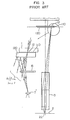
- FIG. 1 A prior art chip-by-chip alignment method is shown in Fig. 1.
- a circuit pattern of a mask or reticle 1 is to be exposed on a chip (or circuit pattern) 21 on a workpiece 2 such as a wafer
- a mirror 560' of alignment detection optical systems 500 and 560' for detecting the target marks must be penetrated into an exposure light flux 41.
- the mirror must be arranged outside of the exposure light flux as shown by 560.
- the wafer circuit pattern 21 and the target marks 22 and 22' may be arranged at positions corresponding to the circuit pattern 11 of the reticle and the target marks 12 and 12' of Fig. 1 as shown in Fig. 2 so that the alignment is attained at the exposure position.
- a distance from the circuit pattern 21 and the wafer target mark 22' must be larger than a predetermined length (1 mm)
- a width W S of an area (scribe area) between adjacent circuit patterns (chips) increases and a yield of the chip decreases and dusts are generated in cutting the chips.
- Fig. 3 shows another prior art exposure position detection measure similar to that disclosed in U.S. Patent No. 4,357,100 issued on November 2, 1982.
- a protection glass 120 is mounted on a pattern surface 110 of a mask (reticle) 1, a light reflected by a target pattern 22 of a wafer 2 and transmitted through a reduction lens 3 is reflected by the protection glass 120 and further transmitted through a light splitting layer 16, and focussed, together with an optical image of the alignment target pattern 12, on a predetermined focusing plane through an enlarging/focusing lens 3', as shown more clearly in the left-hand portion of Fig. 3 representing an enlargement of the encircled part in the right-hand portion of Fig. 3.
- a protection glass is not protected from dusts and a pellicle layer (which is a high molecule layer having a thickness of several microns and which does not influence the imaging characteristic of the reduction lens) is placed on the reticle with a spacing of 6 to 10 mm therefrom.
- the protection glass has a thickness corresponding to such a spacing, the imaging characteristic of the reduction lens is influenced so that the resolution power is lowered.
- a device as shown in Fig. 4A is commercially available.
- an end of a detection system interrupts an exposure light from a circuit pattern A as shown in Fig. 4B, an image of a pattern is defocused if it is to be imaged in the vicinity of a wafer target. Accordingly, the pattern cannot be imaged in the vicinity of the target and only an area inside of a pattern B can be exposed as the circuit pattern.
- an exposure apparatus comprises
- a method of aligning an exposure mask plate with a workpiece having a workpiece alignment mark in an exposure apparatus in which the exposure mask plate includes an exposure pattern area section and an alignment area section and said exposure pattern area section is illuminated by first light source means to project images of patterns contained in an exposure pattern area section through projection lens means onto the workpiece being held on movable stage means comprises the steps of:
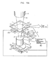
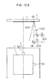
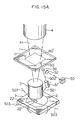
- an exposure apparatus includes an exposure light source 4, a reticle (mask plate means) 1, a projection lens, e.g., a reduction lens 3, a movable stage 7 for holding a photo-sensitive wafer (workpiece) 2 having alignment marks (wafer alignment marks) 22 and 22' and means (not shown) for driving the movable stage 7.
- the reticle 1 includes an exposure pattern area section including an area 11 and alignment/reflection reflection area section including areas 30 and 30' arranged adjacent thereto. Before the exposure pattern area 11 is illuminated by the light source 4 and an image thereof is projected on a chip 21 of a wafer 2 through the reduction lens 3, the alignment of the reticle 1 and the wafer 2 is carried out.
- the alignment/reflection areas 30 and 30' are arranged on that surface of the reticle 1 which does not face the light source 4 and each of the alignment/reflection areas 30 and 30' has a reflection portion and a mask alignment mark portion. Since the areas 30 and 30' are identical in construction and arrangement, only the area 30 is explained below.
- the reflection portion of the area 30 serves as a mirror when an alignment illumination light 501' is projected to the wafer alignment mark 22 adjacent to the chip 21 of the wafer 2 through a semitransparent mirror 55, an enlarging/focussing lens 52 and a mirror 51 and also serves to reflect scattered or reflected light transmitted through the reduction lens 3 from the wafer target mark 22' and direct it to an alignment detection unit 5 disposed out of an exposure light path.
- the reflection portion has a grating and a O-th order light (normal reflection light) is used to illuminate the wafer alignment mark 22 and detect its image.
- O-th order light normal reflection light
- elongated reticle target patterns Cr or Cr2O3 patterns or clear patterns
- the wafer alignment mark illumination light 501' is normally reflected by the reflection portion and directed to a center of the entrance pupil of the reduction lens 3.
- the incident light 501' to the wafer alignment mark 22 or 22' is scanned by a Galvanomirror 53 such that the illumination light falls within the entrance pupil circle.
- the scattered (reflection) light from the wafer alignment mark is focussed onto the alignment/reflection area 30, and after it is normally reflected, the image is refocused onto a detection element unit (imaging element unit) 50 so that a signal shown by a broken line in Fig. 5C is produced.
- the reticle alignment mask portion is illuminated by a reticle target illumination light 503 of another light path through the mirror 54.
- the incident angle of the illumination light to the alignment/reflection area 30 is different from that of the wafer illumination light and the direction of diffraction of the light primarily diffracted by the reflection portion corresponds to the direction of the light from the wafer alignment mark 22.
- a signal shown by a solid line in Fig. 5C is produced by the detection element unit 50.
- the light paths are sequentially switched so that the patterns are detected independently.
- the detected signals are fed to the detecting and processing means 80, in which centers of the waveforms of the detected signals are determined by known measures such as symmetrical pattern matching technique, information on the locations of the waveform centers are once stored in a memory at particular addresses and the positional deviation between the detected signals is determined from the address information.
- a control signal is then produced on the basis of the determined positional deviation and is used to drive the movable stage 7 or a reticle fine adjusting mechanism 130 so that a high precision alignment is attained.
- a control signal For the generation of the control signal, reference may be made to U.S. Patent 4153371 or U.S. Patent 4362389.
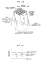
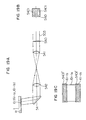
- Figs. 6A and 6B show another arrangement 30-1 of the alignment/reflection area section in the embodiment of the present invention in which the exposure light and the alignment light have substantially the same wavelength, and it is used as the area section 30 of the reticle shown in Fig. 5A.
- the reflection portion 30-1a is mostly coated with Cr or Cr2O3 except a reticle alignment pattern portion 30-1b which has a grating.
- the detection element unit 50 produces a signal as shown in Fig. 6B. In this case, the reticle alignment mark signal is high only for the grated target area.
- Figs. 7A and 7B show another arrangement 30-2 of the alignment/reflection area section in the embodiment of the present invention in which the exposure light and the alignment light have substantially the same wavelength.
- the reflection portion on the reticle has a uniform grating and left and right areas thereof are clear.
- the same detection unit as that of Fig. 5A may be used.
- a reticle signal and a wafer signal as shown in Fig. 7B are produced.
- Figs. 8A and 8B show another arrangement 30-3 of the alignment/reflection area section in the embodiment of the present invention in which the exposure light and the alignment light have substantially the same wavelength.
- a reflection portion 30-3a on the reticle is a uniform Cr or Cr2O3 surface.
- the reticle alignment mark detection illumination light 503 (and the mirror 54) shown in Fig. 5A should not be used and the wafer illumination light is also used to illuminate the reticle.
- An outline or contour 30-3b of the reflection portion 30-3a forms the reticle alignment mark portion, and a signal as shown in Fig. 8B is produced.
- the alignment mark signals of the wafer and the reticle are not simultaneously detected, unlike the embodiments shown in Figs. 5A, 6A and 7A.
- the wafer alignment mark illumination light is directed to the wafer alignment mark through the reduction lens.
- the light may be obliquely directed to the wafer alignment mark from the above of the wafer without passing through the reduction lens, provided that the scattered light from the wafer alignment mark is detected through the reduction lens.
- the alignment/reflection area section including a focusing pattern is arranged in adjacent to the exposure pattern area section as will be explained later, and the focusing pattern is illuminated by an essentially monochromatic light.
- the monochromatic light used need not be a physically pure monochromatic light but a light which can be practically considered as monochromatic may be sufficient for the present purpose.
- a wavelength of the monochromatic light is longer than the wavelength of the ordinary exposure light.
- the light reflected from the focusing pattern illuminated by the monochromatic light is diffracted and forms a condensed image.
- the condensed image is used as the mask alignment mark image.
- the image of the alignment mark on the chip of the wafer is focused in the vicinity of the mask alignment mark by the exposure or projection lens as will be explained later.
- the accurate alignment is attained.
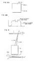
- Fig. 9 shows a relation between image formation at the exposure wavelength of a focusing lens 3 of a semiconductor exposure apparatus and image formation at the alignment wavelength.
- a point P of a recticle 1 is sharply formed on the wafer by the exposure light (g-line) or dotted line light.
- the alignment lights 521 and 522 e-line
- the wafer alignment mark image is formed by the focusing lens 3 at a position P' which is displaced from the position P by ⁇ z.
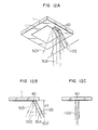
- An alignment/reflection area section including focusing patterns 60 and 60' is formed in a scribe area or bonding areas around an exposure pattern area section 11, in adjacent to the exposure pattern area section 11 on the mask 1.
- the focusing pattern may comprise hyperbolas as shown in Fig. 11A or quasi-hyperbolas as shown in Fig. 11B.
- the pattern comprises a number of hyperbolas or quasi-hyperbolas drawn by shifting a hyperbolar or quasi-hyperbola having a width w in a direction x (direction of a line connecting two focal points of the hyperbola) with a pitch p .
- a black or hatched area represents a Cr surface and a white area represents a Cr-free glass surface.
- the Cr surface forms the reflection portion.
- the width w and the lengths l1, l2, l3, ... of the hatched strips are determined such that they form a group of quasi-hyperbolas which will approximate a group of ideal hyperbolas as much as possible that can be drawn with an electron ray lithography apparatus.
- the alignment mark 22 in Fig. 10, in the scribe area on the wafer or the bonding area in the chip is obliquely illuminated by the e-lines 523 and 524 and the scattered light 503 is transmitted through the imaging lens 3 and the image is focused at the position P' in Fig. 9, directed to the alignment/reflection area section 60 along the light paths 503 and 503' of Fig. 12A, normally reflected (without diffraction) and focused at the position 1122.
- the focusing pattern is formed such that the area 60 and the focusing position 1122 are spaced by ⁇ z from each other.
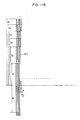
- Fig. 12C is a view looked in a normal direction of the drawing in Fig.
- Fig. 13 shows the slit-shaped condensed image (Fig. 13C) by the diffraction light from the alignment/reflection area section formed in the vicinity of the position 1122 and the image (Fig. 13b) formed by obliquely illuminating the chip 21, transmitting the light therefrom through the focusing lens 3 and normally reflecting the light by the Cr surface of the alignment/reflection area section 60.
- the image from the chip 21 includes two peaks because of the scattered light created by the edges of the mark 22 (22'). Since a mid-point of the two peaks is a center of the mark 22 (22'), ⁇ x determined in a manner shown in Fig. 13d represents a positional deviation of the pattern.
- the deviation is focused onto the alignment detector 50 shown in Fig. 10A by the mirror 53 and the enlarging focusing lens 52 through the light path 504 shown in Figs. 10A and 10B so that an alignment control signal corresponding to the deviation is produced.
- the wafer 2 or the mask 1 is finely moved in accordance with the control signal so that the mask is perfectly aligned with the wafer. Generation of an alignment control signal and attainment of the alignment may be possible in the same manner as in Fig. 5A embodiment.
- the exposure light e.g. g-line
- the exposure light is emitted from the exposure light source means 4 so that the alignment and the exposure are carried out without a time lag and the total wafer exposure time is reduced.
- the alignment/reflection area section having the focusing pattern is arranged on that surface of the mask which does not face the exposure light source, in adjacent to the exposure pattern area section, the image of the reflected diffraction light created by illuminating the focusing pattern with the monochromatic light is detected as the reticle alignment mark image, the image of the alignment mark on the workpiece formed by the scattered light transmitted through the exposure or projection lens is detected and the alignment of those images is attained by driving the means for moving the mask or wafer.
- the mask (reticle) 1 has the exposure pattern area section including the area 11 and has the alignment/reflection area sections including areas 60 and 60' each carrying the focusing patterns, the alignment/reflection area sections being arranged on that surface of the mask 1 which does not face the exposure light source 4, at a position corresponding to the scribe area.
- the focusing pattern comprises hyperbolas or quasi-hyperbolas as shown in Fig. 11A or Fig. 11B.
- the hyperbolas are oriented such that they project toward the circuit pattern.
- the areas 60 and 61' may be rectangles having one side of 0.5 - 1 mm long and they are illuminated by a parallel beam of a He-Ne laser beam source 51 through a mirror 54 (Since the illumination and detection systems for the area 60' are identical to those for the area 60, they are not shown.)
- the He-Ne laser beam diffracted by the focusing pattern is condensed into a slit shape at the position 1122 shown in Fig. 10B.
- the chip 21 to be exposed is on the wafer on the movable wafer stage 7 and under the lens and at a position slightly deviated from the exact wafer position.
- the alignment mark on the scribe area of the wafer 2 is focused at 1122 by obliquely illuminating the alignment mark by the He-Ne laser beams 521 - 524 in four directions, transmitting the lights scattered by the edges of the alignment mark through the focusing lens 3 and normally reflecting the lights by the reflection portion of the area 60, that is, the Cr surface of the focusing pattern.
- the alignment mark image from the wafer formed at 1122 and the condensed image formed by the reflection and diffraction of the light from the mask are enlarged and focused on a detection plane (not shown) of the alignment detector 50 by the mirror 53 and the enlarging focusing lens 52 to determine the registration of both alignment mark images.
- the detection may be made by a solid-state imaging device or a combination of a scanning slit and a photo-multiplier. Misregistration of both patterns is detected and the control signal is generated.
- the wafer stage 7 or the mask 1 is moved in accordance with the control signal, and when the registration is attained, the exposure is carried out. Since the exposure light 41 is completely isolated from the alignment optical system and does not interfere, the exposure is completed immediately after the alignment.
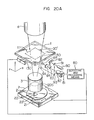
- Figs. 14A and 14B show another embodiment of the present invention.
- the like elements to those shown in Figs. 10A and 10B are designated by the like numerals.
- the focusing patterns in the areas 60 and 60' of the alignment/reflection area sections adjacent to the exposure pattern area section including area 11 of the mask 1 are arranged at free locations in the bonding area in the exposure pattern area.
- the light from the e-line illumination light source 51'' of the mercury lamp is transmitted through the semitransparent mirror 56 along the light path 501, normally reflected by the reflection portion of the alignment/reflection area 60 including the focusing pattern such as that shown in Figs.
- the mask position may be determined by directing the monochromatic light 502 emitted from the He-Ne laser beam source, an Ar laser beam source or the e-line light source 51' to the alignment/reflection area 60 through the mirror 54 and detecting the slit-shaped image at 1122 by the diffraction light from the focusing pattern.
- the detection of the alignment mark images of the mask 1 and the wafer 2 and the alignment control are identical to those described in the above embodiment.
- Figs. 15A and 15B show another embodiment of the present invention.
- the like elements to those shown in Figs. 10A and 10B are designated by the like numerals.
- the light emitted from the semiconductor laser 51'' obliquely illuminates the alignment/reflection area 60 on the mask 1. Since the wavelength of the light is long, a primary diffraction angle is large and the primary diffracted light is returned in the incident direction and focused into a slit shape at position 1122.
- the light normally reflected by the reflection portion of the area 60 including the pattern as shown in Figs. 11A and 11B is transmitted along the light path 503' and used to illuminate the alignment mark in the scribe area of the wafer.
- the alignment mark of the wafer may be obliquely illuminated by the laser beams 521 - 524 in four directions, and the scattered light created by the step of the alignment mark of the wafer or the reflection light created by the illumination is normally reflected by the reflection portion of the area 60 and focused at 1122 as may be done in the previous embodiment.
- the detection of the signals of the alignment mark images of the mask and the wafer and the alignment control are now explained.
- Fig. 16 shows another arrangement of the alignment/reflection area section formed on the mask. It is particularly suitable for use in the exposure apparatus shown in Fig. 5A although it may be used in the exposure apparatus shown in other drawings.
- the alignment/reflection area section 61 has a reflection portion 61-1a at a center of the pattern and an alignment portions 61-1b including a focusing pattern at its side peripheries.
- the focusing pattern comprises a group of curves drawn by shifting a portion of a hyperbola in y-direction at a constant pitch, that is, a pattern of a group of hyperbolas.
- an electron beam lithography apparatus is usually used.
- the pattern is fine, it is difficult to smoothly draw a curved pattern. Accordingly, small rectangles having sides along the x-direction and y-direction may be arranged to simulate the hyperbola.
- the alignment/reflection area section 61 shown in Fig. 16 is arranged in the same manner as the alignment/reflection area 60 shown in Fig. 5A is arranged to align the wafer with the mask.
- the alignment light has a wavelength different from that of the exposure light, unlike in Fig. 5A embodiment.
- the wafer alignment mark is illuminated by directing the laser illumination light 501' through the galvanomirror 53, the beam splitter 55, the focusing lens 52 and the mirror or beam splitter 51 to the reflection portion 61-1a (Fig.
- the position of the image formed is determined by the wavelength of the laser beam 501' used for the alignment and a chromatic aberration of the reduction lens 3.
- the alignment/reflection area 61 has the center reflection portion 61-1a and the peripheral alignment mark portions 61-1b which contains the pattern of hyperbolas.
- the linear image 1122 is formed at the position of the image of the wafer alignment mark.
- a shape of the hyperbolas and a strength distribution of the linear image (change in the x-direction) for forming the linear image at the focusing positon of the wafer alignment mark (spaced from the lower surface of the reticle by h ) are now explained with reference to Figs. 17A - 17C.
- Fig. 17A shows the alignment/reflection area 61 on the reticle 1 and coordinates (x, y) exist on this plane.
- the mask alignment marks 61-1b which include the focusing patterns, that is, the hyperbola patterns (hyperbola gratings) are arranged on the opposite sides of the reflection portion 61-1a. Broken lines shown in the reflection portion 61-1a merely show connections of the left and right hyperbolas and they are not real patterns.
- Figs. 17B and 17C are side views of Fig. 17A, and x-y coordinates and y-z coordinates exist on the respective planes.
- the incident laser beam is a collimated beam which is in the y-z plane, makes an angle ⁇ 0 with the z-axis, is reflected and diffracted by the pattern of hyperbolas arranged at a pitch p to form the linear pattern 1122 at the position spaced from the lower surface of the reticle by h .
- the optical axis of the diffraction light makes an angle ⁇ 1 with the z-axis.
- the pattern of hyperbolas is represented by the following formula. where n is an integer. It is an aggregation of hyperbolas whose asymptotic curve is given by the following formula.
- the pitch p of the hyperbolas is given by This hyperbola grating (hyperbola pattern) does not exist in the reflection portion 61-1a as shown in Fig. 17A (broken lines) but exists in the alignment mark portions 61-1b on the opposite sides of the reflection area 61-1a.
- a width of the reflection portion 61-1a is represented by Wm and a total width of the hyperbola pattern (including the width of the reflection portion 61-1a) is represented by Wg.
- the width Wm should be at least a width of the illumination beam for the wafer alignment mark.
- the reflection portion 61-1a is too narrow and the illumination beam illuminates the hyperbola pattern, the reflected diffraction light therefrom is superimposed on the wafer alignment mark and an S/N ratio of a detection signal for the wafer alignment mark is reduced.
- the width is approximately equal to a product of a diameter of an illumination area necessary to detect the wafer alignment mark and a reciprocal of a reduction factor of the reduction lens.
- the reflected diffraction beam forms the linear image extending along the y-axis at the position spaced from the mask surface by h , as shown in Figs. 17B and 17C.
- An intensity distribution I(X) in the x-direction (coordinate on the linear image is X) is given by where C is a constant proportional to a laser beam intensity and a reflection factor. It is a pattern of a square of cosine waves having zero phase at a center of the pattern and having an envelope represented by I e 2 as shown by a broken line in Fig. 18.
- the center of the pattern can be precisely determined so that the position of the mask can be precisely determined.
- this pattern is formed on the same focusing plane ( h below the reticle surface) as that of the wafer alignment mark image formed by illuminating the wafer alignment mark by the laser beam and enlarging the image by the reduction lens (after the reflection by the reflection portion of the alignment/reflection area). Accordingly, as shown in Fig. 5A, it can be detected by the same detection system as that for the wafer alignment mark, by using the solid-state array device 50 through the mirror 51, focusing lens 52 and beam splitter 55.
- a drift of the detection position with time is zero as compared with a case where the marks are detected by two separate detection optical systems, and the optical system can be simplified and rendered inexpensive.
- the wafer target alignment mark and the diffraction image of the hyperbola pattern representing the reticle position are time-serially detected by the same detection system.
- the wafer 2 is moved by the array pitch of the chip by the x-y movable stage (wafer table) 7 so that an unexposed chip is brought under the reduction lens.
- the wafer alignment mark illumination laser beam 501' first illuminates the wafer alignment mark 22 so that the position thereof is detected by the solid-state array device 50.
- the laser beam 501' is extinguished and the illumination light 503 illuminates the alignment/reflection area (hyperbola pattern) on the reticle so that the reticle position is detected by the solid-state array device 50.
- a relative deviation is determined based on the two detected positons and it is compensated by finely adjusting the reticle 1 by the reticle (mask) fine adjusting mechanism 130. Since the distance of fine adjustment is the product of the reciprocal of the reduction factor of the reduction lens and the distance of the relative movement of the wafer 2, precise positioning is attained as compared to a case where the wafer 2 is moved. Since the positions of the wafer and the mask are time-serially detected, both detection patterns can be independently detected and the S/N ratio is not lowered by the other pattern. Thus, high precision detection is attained.
- the collimated laser beam is irradiated to the alignment/reflection area 61 at the incident angle ⁇ 0 when the reticle position is to be detected, but the light normally reflected by the area 61 is transmitted through the reduction lens 3 and illuminates the wafer alignment mark.
- the wafer alignment mark image may be superimposed on the diffraction linear image of the hyperbola pattern. This does not pose a substantial problem when the intensity of the diffraction linear image is high, but the influence of the superposition on the alignment precision cannot be neglected if the intensity of the reflection image of the wafer alignment mark is high or an extremely high alignment precision is required.
- the width W m of the reflection portion 61-1a of the area 61 shown in Figs. 17A to 17C is selected to a minimum required to illuminate the wafer alignment mark, and the width W g is selected to where NA is the number of aperture of the detection optical system. In this manner, W g -W m is selected to be large. As a result, a peak of the intensity of the hyperbola grating diffraction image (Fig. 18) is proportional to (W g -W m )2 and the reduction of the S/N ratio due to the superposition of the wafer pattern image is avoided.
- the recticle pattern of Fig. 16 does not use the conventional Cr mask but uses the Cr2O3 mask.
- the intensity I w of the wafer alignment mark image is proportional to r2 because the light is reflected twice in the illumination cycle and the imaging cycle.
- the intensity I m of the hyperbola pattern diffraction image representing the reticle position is proportional to r because the diffraction image is obtained by one reflection by the mask.
- a ratio of the intensity of the mask alignment mark diffraction image and the intensity of the wafer alignment mark image (noise image in detecting the mask alignment mark diffraction image), that is, the S/N ratio is given by Accordingly, the smaller the mask reflection factor is, the higher is the S/N ratio.
- the S/N ratio when the Cr2O3 mask is used is approximately four times as large as that when the Cr mask is used.
- Other low reflection factor materials than Cr2O3 may be used to attain the same effect. The effect will be satisfactory if the S/N ratio is at least three times as high as that obtained when the Cr mask is used.
- FIGs. 19A - 19C A third solution is shown in Figs. 19A - 19C. If the laser beam is irradiated only to the hyperbola pattern 61-1b on the opposite sides of the reflection portion 61-1a of the alignment/reflection area 61 and not irradiated to the wafer alignment mark 22, the wafer alignment mark image is not superimposed as the noise.
- a restrictive illumination mask 540 is inserted in the light path of the collimated illumination light beam 503 so that only the alignment mark portion 61-1b of the area 61 on the reticle 1.
- the mask 540 transmits the light in the area (openings) corresponding to the hyperbola pattern area and blocks the light in other areas.
- Fig. 19C illustrates how the area 61 in Fig. 19A is illuminated by the light 503 masked by the mask 540.
- the alignment portions 61-1b carrying hyperbolic patterns receive light 5401' representative of the images of the openings 5401.
- the focusing position of the wafer alignment mark image and the position of the diffraction image of the hyperbola pattern representing the reticle position are intentionally shifted from each other on the focusing plane.
- the amount of shift depends on the alignment precision in the step-and-repeat process of the wafer table and is to be larger than the line width of the wafer alignment mark.
- the mark or pattern is formed such that the wafer alignment mark and the diffraction image of the hyperbola pattern representing the reticle position are relatively shifted from each other by the above shift amount.
- the illumination light for the hyperbola pattern may be slightly shifted from the right angle by an angle made thereby with the x-axis as shown in Figs. 17A and 17C.
- the g-line, e-line and d-line which are spectrum lines of the mercury lamp or the He-Ne laser beam is used to align the patterns of the mask and the wafer.
- Such a light is irradiated through the exposure focusing lens. Since the exposure focusing lens is usually designed to exhibit a best focusing characteristic (high resolution power) only to the monochromatic light such as g-line, the spectrum width of the illumination light other than the exposure light must be narrow. However, for the light other than the exposure light, the focusing position on the optical axis varies significantly even for a slight change of the wavelength.
- the alignment detection pattern in order to attain the alignment detection pattern with a high resolution, it is necessary to use the light of as narrow spectrum width as possible.
- the light source other than the laser such as the mercury lamp cannot produce a light having a sufficiently narrow spectrum width and a sufficient intensity to allow the detection of the alignment mark on the wafer.
- the laser beam since the laser beam usually has a high coherence (spatial coherence), if the alignment mark on the wafer is marked by granular material such as Al or WSi, a noise called a speckle pattern is included in the mark image detection signal and the S/N ratio of the detection signal is lowered.
- a fine variation of the thickness of the resist layer may appear as a noise so that the S/N ratio of the detection signal is lowered.
- the alignment light has a wavelength different from that of the exposure light.
- Alignment/reflection area sections including areas 30 and 30' on the mask (reticle) 1 may contain the focusing patterns shown in Figs. 10A, 10B, 11A, 11B, 12A-12C and 13 and may be arranged on the mask 1 in the manner shown in those figures.
- Numeral 4 denotes an exposure light source.
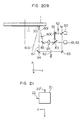
- the light emitted from the laser beam source 90 is split by the beam splitter 91.
- One of the split beams illuminates the alignment/reflection area 30 containing the hyperbola pattern.
- the illumination light is diffracted and a primary diffraction light passes through a light path 601 and focused into a linear image at 600.
- the direction (x-direction) of the linear image represents the x-direction of the reticle 1.
- the other of the split beams is deflected by a Galvanomirror 92 which is an incident angle varying means.
- the deflected beam passes through a semitransparent mirror 83, a lens 84 and a mirror 85 and is directed to the alignment/reflection area 30 adjacent to the exposure pattern area 11 of the mask (reticle) 1, and the normally reflected light therefrom is directed into an entrance pupil 205 of the exposure focusing lens 3.
- the light 612 transmitted through the entrance pupil illuminates the alignment mark 22 (22') on the wafer arranged in the periphery of the chip 21 on the wafer 2.
- the chip 21 on the wafer 2 includes the elongated alignment marks 22 and 22' extending in the y-direction and the x-direction as shown in Fig.
- Figs. 20A and 20B only a control unit including an optical system for aligning the alignment mark 30 on the reticle 1 with the alignment mark 22 on the wafer 1 is shown as the alignment optical system, and another control unit including an optical system for aligning the mark 30' with the mark 22' is omitted because it may be identical.
- the laser beam directed to the alignment mark 22 on the wafer 1 in Figs. 20A and 20B has no change of incident angle in the x-z plane (x-direction) normal to the lengthwise direction of the alignment mark as shown in Fig. 22B, but the incident angle changes in the y-z plane (y-direction) normal to the mask 1 or the wafer 2 as shown in Fig. 22C.
- Fig. 22B shows a view of the alignment mark 22 on the wafer 2 (underlying layer of the alignment mark) as viewed in a direction A shown in Fig. 22A
- Fig. 22C is a view as viewed in a direction B.
- Numeral 43 in Figs. 22B and 22C denotes a resist film coated on the wafer 2.
- the light including the position information of the alignment mark 22 reflected by the wafer 2 is usually a diffraction pattern spreading in a direction (x-direction) normal to the lengthwise direction (y-direction) of the alignment mark on the wafer 1, as shown by 220, 221 and 222 in Fig. 23A, on the entrance pupil 205 of the exposure focusing lens 3 (x-y plane parallel to the mask 1 or the wafer 2). Accordingly, by deflecting the incident angle to the y-direction (normal to the x-axis) in the y-z plane as shown in Fig.
- the diffraction light information particularly the position information of the pattern to be detected (x-coordinate for the alignment mark 22 and y-coordinate for the mark 22') can be detected without loss.
- Fig. 23B shows the light deflected in the normal direction (x-direction in the z-x plane). In this case, the information in the direction to be detected is lost. The incident light is deflected in the direction shown in Figs.
- reticle alignment mark image The reticle alignment mark image and the wafer alignment mark image are transmitted through the mirror 85, lens 84 and beam splitter 83 and refocused on the imaging plane of the imaging means 81 by the focusing optical system 82.
- the wafer alignment mark image 22 and the mask alignment mark image 30 focused on the imaging plane of the imaging means 81 are shown in Fig. 25, in which numeral 600 denotes the imaging plane, numeral 30 denotes the image of the reticle window 30, and numeral 22 denotes the image of the alignment mark 22 of the wafer 2.
- a light intensity I t (i, j) is detected at time t for an address (i, j) of the array pixels.
- the detection signals in the longitudinal direction of the alignment mark 22 are summed. so that the signals are averaged and the S/N ratio is improved.
- the S/N ratio of the detection signal is still low even after the averaging as shown in Figs. 26A and 26B, in which the incident angles of the illumination light are fixed at different angles.
- the incident angle ⁇ is changed from time to time in the plane described above.
- the detection signal in the i-direction O ⁇ (i) is now represented by the following expression: Since the accumulation is usually done in the conventional imaging means, no special means is required.
- Figs. 27A - 27C show other modes of changing the incident angle to the wafer alignment mark.
- the incident angle is set by a step function
- Figs. 27B and 27C the incident angles are fixed depending on the alignment marks.
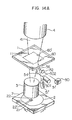
- Figs. 28A and 28B illustrate the illumination of the alignment mark in the multiple interference environment.
- ⁇ 514 nm
- the signal intensity changes as shown in Figs. 30A, 30B and 30C (which show the intensities detected in the x-direction when the resist layer thickness changes only depending on the shape of the underlying layer and is symmetric, or changes in accordance with the edge of the pattern).
- the signal ⁇ O is superimposed as the noise on the signals of Figs. 30A - 30C so that misdetection of the edge may occur when ⁇ O is large.
- I R denotes the reticle alignment mark image
- I W denotes the wafer alignment mark image.
- a deviation between the centers of those signal waveforms is detected by the detection system 80 and the wafer table 7 is moved in the x-direction (and also in the y-direction) to compensate for such deviation.
- shutters 62 and 63 are inserted in the respective light paths to detect the lights separately so that the centers of the signals I R and I W can be detected without error.
- Generation of the alignment control signal and alignment may be attained in the same manner as described with reference to Fig. 5A embodiment.
- a two-dimensional imager means such as a solid-state camera to detect images of wafer alignment marks and reticle alignment marks.
- these images carry only one-dimensional information, detection of these images is possible at a high speed and with a high resolution by the provision of a cylindrical lens before the imager means for compressing the lengthwise information of the images of the elongated or slender alignment marks and by the use of a one-dimensional array of imaging elements (e.g. CCD) for the imager means.
- the cylindrical lens and one-dimensional array may be, e.g., those disclosed in printed Japanese publications, Japanese Patent Publication No. 29045/83 or 53217/81.
- the alignment mark on the wafer is illuminated by the laser beam having the narrow spectrum width so that the defocusing due to the chromatic aberration of the exposure focusing lens is minimized and the level of the detection signal is kept sufficiently high.
- the incident angle of the laser beam can be controlled to an optimum angle in accordance with the semiconductor process such as the material of the resist layer, the thickness thereof, the shape of the underlying layer and the material thereof so that the noise due to the coherence of the laser beam is substantially reduced. Accordingly, the stability of the detection of the alignment pattern is significantly improved.
Claims (16)
- Dispositif d'exposition, comprenant- des premiers moyens formant source de lumière (4);- des moyens (1) en forme de plaque formant masque possédant un premier élément de surface de motifs d'exposition (11) et un élément de surface d'alignement (30,30') adjacent audit élément de surface de motifs d'exposition et comprenant une partie formant repère d'alignement du masque, et
disposés de manière que ledit élément de surface de motifs d'exposition est éclairé par lesdits premiers moyens formant source de lumière;- des moyens formant table mobile (7) servant à retenir sur eux une pièce à usiner (2) possédant un repère (22,22') d'alignement de la pièce à usiner;- des moyens formant lentille de projection (3)
intercalés entre lesdits moyens en forme de plaque formant masque et lesdits moyens formant table mobile, et disposés devant lesdits moyens en forme de plaque formant masque pour lesdits premiers moyens formant source de lumière de sorte que, lorsqu'il est éclairé, ledit élément de surface de motifs d'exposition est projeté sur ladite pièce à usiner par lesdits moyens formant lentille de projection;- des moyens d'alignement
pour détecter la relation de position entre ladite partie formant repère d'alignement du masque dudit élément de surface d'alignement dans lesdits moyens en forme de plaque formant masque et ledit repère d'alignement de ladite pièce à usiner sur lesdits moyens formant table mobile, et
pour produire un signal de commande pour réaliser l'alignement de ladite partie formant repère d'alignement du masque sur ledit repère d'alignement de la pièce à usiner, et- des moyens d'entraînementcaractérisé en ce que
destinés à régler la position relative entre lesdits moyens en forme de plaque formant masque et ladite pièce à usiner, et
adaptés pour répondre audit signal de commande;
que ledit élément de surface d'alignement (30,30') comporte en outre à la fois une partie réfléchissante et une partie de diffraction,
que ledit élément de surface de motifs d'exposition et ledit élément de surface d'alignement sont disposés sur la surface desdits moyens en forme de plaque formant masque, qui n'est pas tournée vers lesdits moyens formant source de lumière (4), et que lesdits moyens d'alignement comprennent(a) des seconds moyens formant source de lumière (503;521 à 524;51'';90) disposés par rapport auxdits moyens en forme de plaque formant masque de sorte que la lumière délivrée par lesdits seconds moyens formant source de lumière est dirigée de manière à éclairer ledit repère d'alignement du masque et ledit repère d'alignement de la pièce à usiner de telle sorte que la lumière réfléchie résultante dudit repère d'alignement de la pièce à usiner est dirigée sur ledit élément de surface d'alignement par l'intermédiaire desdits moyens formant lentille de projection (3) et est réfléchie sur ladite partie réfléchissante de manière à former une image réfléchie dudit repère d'alignement de la pièce à usiner, et(b) des moyens de détection (5;50,52,54,56; 80 à 85) servant à détecter ladite image réfléchie dudit repère d'alignement de la pièce à usiner et une image de ladite partie formant repère d'alignement du masque dudit élément de surface d'alignement pour produire ledit signal de commande. - Dispositif selon la revendication 1, caractérisé en ce
que la longueur d'onde de la lumière délivrée par lesdits seconds moyens formant source de lumière (503) est sensiblement égale à celle de la lumière délivrée par lesdits premiers moyens formant source de lumière (4), et
que ledit élément de surface d'alignement (30, 30') possède un contour prédéterminé. - Dispositif selon la revendication 2, caractérisé en ce
que ledit contour dudit élément de surface d'alignement (30,30') constitue ladite partie formant repère d'alignement du masque. - Dispositif selon la revendication 2, caractérisé en ce
que ledit élément de surface d'alignement (30, 30') comprend des moyens en forme de réseau constituant ladite partie formant repère d'alignement du masque. - Dispositif selon la revendication 1, caractérisé en ce
que la longueur d'onde de la lumière délivrée par lesdits seconds moyens formant source de lumière (521 à 524) diffère de celle de la lumière délivrée par lesdits premiers moyens formant source de lumière (4), et
que ledit élément de surface d'alignement (30, 30') comprend un groupe de lignes sensiblement hyperboliques (60) servant à former une image de diffraction représentative de ladite partie formant repère d'alignement du masque. - Dispositif selon la revendication 5, caractérisé en ce
que ledit groupe de lignes hyperboliques (60) est orienté de manière à projeter la lumière en direction dudit élément de surface de motifs d'exposition dans lesdits moyens en forme de plaque formant masque (1). - Dispositif selon la revendication 1, caractérisé en ce
que la longueur d'onde de la lumière délivrée par lesdits seconds moyens formant source de lumière (521 à 524) diffère de celle de la lumière délivrée par lesdits premiers moyens formant source de lumière (4),
que ladite partie formant repère d'alignement du masque est constituée de première et seconde sous-parties d'alignement (61-1b) entre lesquelles est interposée ladite partie réfléchissante (61-1a), et
que lesdites première et seconde sous-parties d'alignement portent des parties d'un groupe de lignes hyperboliques servant à former, lorsqu'elles sont éclairées, une image représentative de ladite partie formant repère d'alignement du masque. - Dispositif selon la revendication 1, caractérisé en ce
que lesdits moyens d'alignement comprennent en outre(c) des moyens (92) accouplés optiquement auxdits seconds moyens formant source de lumière (90) pour modifier l'angle d'incidence de la lumière éclairant ledit repère (22,22') d'alignement de la pièce à usiner, dans un plan perpendiculaire auxdits moyens en forme de plaque formant masque (1) et parallèle à la direction longitudinale dudit repère d'alignement de la pièce à usiner, etque lesdits moyens de détection comprennent des moyens pour accumuler la lumière réfléchie par ledit repère d'alignement de la pièce à usiner et reçue par l'intermédiaire de ladite partie réfléchissante dudit élément de surface d'alignement (30,30'). - Dispositif selon la revendication 1, caractérisé en ce
que lesdits seconds moyens formant source de lumière (521 à 524) sont disposés de manière à permettre à la lumière d'éclairer obliquement ledit repère d'alignement de la pièce à usiner sans traverser lesdits moyens formant lentille de projection (3). - Dispositif selon la revendication 1, caractérisé en ce
que lesdits seconds moyens formant source de lumière (503;51'';90) sont disposés de manière à diriger la lumière tout d'abord sur ledit élément de surface d'alignement (30;60) de manière qu'elle soit réfléchie par la partie réfléchissante de cet élément de surface et dirigée, par l'intermédiaire desdits moyens formant lentille de projection (3) sur ledit repère (22,22') d'alignement de la pièce à usiner afin d'éclairer ce repère. - Procédé d'alignement d'une plaque formant masque d'exposition (1) avec une pièce à usiner (2) possédant un repère (22,22') d'alignement de cette pièce, dans un dispositif d'exposition dans lequel la plaque formant masque d'exposition comprend un élément de surface de motifs d'exposition et un élément de surface d'alignement, et ledit élément de surface de motifs d'exposition est éclairé par lesdits premiers moyens formant source de lumière (4) de manière à projeter des images de motifs contenus dans un élément de surface de motifs d'exposition (11), par l'intermédiaire de moyens formant lentille de projection (3) sur la pièce à usiner (2) maintenue sur des moyens en forme de table mobile (7), ledit procédé comprenant les étapes consistant à- éclairer ledit élément de surface d'alignement de ladite plaque formant masque et ledit repère (22,22') d'alignement de la pièce à usiner;- détecter la relation de position entre ladite partie formant repère d'alignement et ledit repère d'alignement de la pièce à usiner;- produire un signal de commande représentatif d'un défaut d'alignement entre ladite partie formant repère d'alignement et ledit repère d'alignement de la pièce à usiner et tiré de la relation de position détectée; et- régler la position relative entre ladite plaque formant masque d'exposition et ladite pièce à usiner en fonction dudit signal de commande,caractérisé en ce
que pour ladite étape d'éclairement, ledit élément de surface d'alignement (30;60) est agencé de manière à être adjacent audit élément de surface de motifs d'exposition sur la surface de ladite plaque formant masque d'exposition (1), qui n'est pas tournée vers lesdits premiers moyens formant source de lumière (4), ledit élément de surface d'alignement comprenant une partie formant repère d'alignement et une autre partie comprenant des portions réfléchissantes et des portions réalisant une diffraction, et
que ledit éclairage dudit élément de surface d'alignement de ladite plaque formant masque et dudit repère d'alignement de la pièce à usiner est exécuté par des seconds moyens formant source de lumière (503, 521 à 524; 51''; 90) de sorte que la lumière réfléchie sur ledit repère d'alignement de la pièce à usiner traverse lesdits moyens formant lentille de projection (3) et est réfléchie sur ladite portion réfléchissante de ladite autre partie comprenant une portion réfléchissante et une portion réalisant une diffraction. - Procédé selon la revendication 11, caractérisé en ce
que pendant l'étape d'éclairage dudit repère d'alignement de la pièce à usiner, l'angle d'incidence (0) de la lumière éclairant ledit repère (22,22') d'alignement de la pièce à usiner est modifié dans un plan perpendiculaire à ladite plaque formant masque d'exposition (1) et parallèle à la direction longitudinale dudit repère d'alignement de la pièce à usiner. - Procédé selon la revendication 11, caractérisé en ce
que la lumière servant à éclairer ledit repère (22,22') d'alignement de la pièce à usiner est amenée à traverser lesdits moyens formant lentille de projection (3). - Procédé selon la revendication 11, caractérisé en ce
que la lumière servant à éclairer ledit repère (22,22') d'alignement de la pièce à usiner est dirigée sur repère sans traverser lesdits moyens formant lentille de projection (3). - Procédé selon la revendication 11, caractérisé en ce
que ladite: partie formant repère d'alignement comprend un motif en forme de réseau, et
que lesdits seconds moyens formant source de lumière (521 à 524; 51''; 90) peuvent émettre une lumière sensiblement monochromatique possédant une longueur d'onde différente de celle de la lumière délivrée par lesdits premiers moyens formant source de lumière (4). - Procédé selon la revendication 15, caractérisé en ce
que ledit motif en forme de réseau est formé par un groupe de lignes sensiblement hyperboliques (60).
Applications Claiming Priority (4)
| Application Number | Priority Date | Filing Date | Title |
|---|---|---|---|
| JP58243866A JPH0612753B2 (ja) | 1983-12-26 | 1983-12-26 | パターン検出方法及びその装置 |
| JP243866/83 | 1983-12-26 | ||
| JP59222010A JPS61100931A (ja) | 1984-10-24 | 1984-10-24 | 縮小投影式アライメント方法 |
| JP222010/84 | 1984-10-24 |
Publications (3)
| Publication Number | Publication Date |
|---|---|
| EP0148477A2 EP0148477A2 (fr) | 1985-07-17 |
| EP0148477A3 EP0148477A3 (en) | 1985-09-04 |
| EP0148477B1 true EP0148477B1 (fr) | 1991-09-04 |
Family
ID=26524628
Family Applications (1)
| Application Number | Title | Priority Date | Filing Date |
|---|---|---|---|
| EP84115889A Expired - Lifetime EP0148477B1 (fr) | 1983-12-26 | 1984-12-20 | Appareil d'exposition ainsi que méthode d'alignement d'un masque avec une pièce de travail |
Country Status (4)
| Country | Link |
|---|---|
| US (1) | US4668089A (fr) |
| EP (1) | EP0148477B1 (fr) |
| KR (1) | KR900001269B1 (fr) |
| DE (1) | DE3485022D1 (fr) |
Families Citing this family (46)
| Publication number | Priority date | Publication date | Assignee | Title |
|---|---|---|---|---|
| US4937618A (en) * | 1984-10-18 | 1990-06-26 | Canon Kabushiki Kaisha | Alignment and exposure apparatus and method for manufacture of integrated circuits |
| US4828392A (en) * | 1985-03-13 | 1989-05-09 | Matsushita Electric Industrial Co., Ltd. | Exposure apparatus |
| JPH0616480B2 (ja) * | 1985-06-03 | 1994-03-02 | 株式会社日立製作所 | 縮小投影式アライメント方法およびその装置 |
| US4771180A (en) * | 1985-10-11 | 1988-09-13 | Matsushita Electric Industrial Co. Ltd. | Exposure apparatus including an optical system for aligning a reticle and a wafer |
| JPH0685387B2 (ja) * | 1986-02-14 | 1994-10-26 | 株式会社東芝 | 位置合わせ方法 |
| JPH0785466B2 (ja) * | 1986-07-04 | 1995-09-13 | キヤノン株式会社 | 位置合せ装置 |
| US4943733A (en) * | 1987-05-15 | 1990-07-24 | Nikon Corporation | Projection optical apparatus capable of measurement and compensation of distortion affecting reticle/wafer alignment |
| JPH065663B2 (ja) * | 1987-06-30 | 1994-01-19 | 株式会社日立製作所 | 半導体露光方法及びその装置 |
| JPH01189503A (ja) * | 1988-01-25 | 1989-07-28 | Hitachi Ltd | パターン検出方法及びその装置 |
| US5340992A (en) * | 1988-02-16 | 1994-08-23 | Canon Kabushiki Kaisha | Apparatus and method of detecting positional relationship using a weighted coefficient |
| US5094539A (en) * | 1988-03-07 | 1992-03-10 | Hitachi, Ltd. | Method of making semiconductor integrated circuit, pattern detecting method, and system for semiconductor alignment and reduced stepping exposure for use in same |
| US5260771A (en) * | 1988-03-07 | 1993-11-09 | Hitachi, Ltd. | Method of making semiconductor integrated circuit, pattern detecting method, and system for semiconductor alignment and reduced stepping exposure for use in same |
| US5155370A (en) * | 1988-09-09 | 1992-10-13 | Canon Kabushiki Kaisha | Device for detecting the relative position of first and second objects |
| JP2650396B2 (ja) * | 1989-02-07 | 1997-09-03 | キヤノン株式会社 | 位置検出装置及び位置検出方法 |
| JPH032504A (ja) * | 1989-05-30 | 1991-01-08 | Nikon Corp | 位置合わせ装置 |
| US5053628A (en) * | 1989-07-13 | 1991-10-01 | Matsushita Electric Industrial Co., Ltd. | Position signal producing apparatus for water alignment |
| FR2656700B1 (fr) * | 1989-12-28 | 1992-08-07 | Aerospatiale | Procede de restitution du mouvement d'un mobile par observation d'un symbole forme sur ce dernier et dispositifs pour la mise en óoeuvre du procede. |
| US5357311A (en) * | 1991-02-25 | 1994-10-18 | Nikon Corporation | Projection type light exposure apparatus and light exposure method |
| JP3210123B2 (ja) * | 1992-03-27 | 2001-09-17 | キヤノン株式会社 | 結像方法及び該方法を用いたデバイス製造方法 |
| US5274420A (en) * | 1992-04-20 | 1993-12-28 | International Business Machines Corporation | Beamsplitter type lens elements with pupil-plane stops for lithographic systems |
| KR970003593B1 (en) * | 1992-09-03 | 1997-03-20 | Samsung Electronics Co Ltd | Projection exposure method and device using mask |
| JP3195200B2 (ja) * | 1994-12-09 | 2001-08-06 | キヤノン株式会社 | 半導体露光装置および異物検出方法 |
| JP3450509B2 (ja) * | 1995-04-13 | 2003-09-29 | キヤノン株式会社 | 投影露光装置及び該装置を用いて素子を製造する方法 |
| US6270947B2 (en) * | 1999-04-30 | 2001-08-07 | Infineon Technologies Ag | Method and apparatus for reducing non-uniformity area effects in the manufacture of semiconductor devices |
| GB2356786B (en) * | 1999-11-29 | 2003-09-03 | Marconi Electronic Syst Ltd | Method and apparatus for aligning a crystalline substrate |
| JP4414535B2 (ja) * | 2000-01-13 | 2010-02-10 | 進 野田 | 半導体装置の製造方法 |
| US6700096B2 (en) * | 2001-10-30 | 2004-03-02 | Semiconductor Energy Laboratory Co., Ltd. | Laser apparatus, laser irradiation method, manufacturing method for semiconductor device, semiconductor device, production system for semiconductor device using the laser apparatus, and electronic equipment |
| TWI289896B (en) * | 2001-11-09 | 2007-11-11 | Semiconductor Energy Lab | Laser irradiation apparatus, laser irradiation method, and method of manufacturing a semiconductor device |
| TWI291729B (en) | 2001-11-22 | 2007-12-21 | Semiconductor Energy Lab | A semiconductor fabricating apparatus |
| US7133737B2 (en) | 2001-11-30 | 2006-11-07 | Semiconductor Energy Laboratory Co., Ltd. | Program for controlling laser apparatus and recording medium for recording program for controlling laser apparatus and capable of being read out by computer |
| JP3934536B2 (ja) * | 2001-11-30 | 2007-06-20 | 株式会社半導体エネルギー研究所 | レーザ照射装置およびレーザ照射方法、並びに半導体装置の作製方法 |
| US6979605B2 (en) * | 2001-11-30 | 2005-12-27 | Semiconductor Energy Laboratory Co., Ltd. | Manufacturing method for a semiconductor device using a marker on an amorphous semiconductor film to selectively crystallize a region with a laser light |
| US7214573B2 (en) | 2001-12-11 | 2007-05-08 | Semiconductor Energy Laboratory Co., Ltd. | Method of manufacturing a semiconductor device that includes patterning sub-islands |
| JP4282985B2 (ja) * | 2002-12-27 | 2009-06-24 | 株式会社半導体エネルギー研究所 | 表示装置の作製方法 |
| KR100531416B1 (ko) * | 2003-09-17 | 2005-11-29 | 엘지.필립스 엘시디 주식회사 | Sls 장비 및 이를 이용한 실리콘 결정화 방법 |
| US7385671B2 (en) * | 2004-05-28 | 2008-06-10 | Azores Corporation | High speed lithography machine and method |
| JP2007142275A (ja) * | 2005-11-21 | 2007-06-07 | Toshiba Corp | フォトマスクの判定方法、半導体装置の製造方法及びプログラム |
| DE102006003535A1 (de) * | 2006-01-24 | 2007-08-02 | Schott Ag | Verfahren zur Temperaturbeeinflussung einer Schmelze |
| DE102008048660B4 (de) * | 2008-09-22 | 2015-06-18 | Carl Zeiss Sms Gmbh | Verfahren und Vorrichtung zur Vermessung von Strukturen auf Photolithographiemasken |
| NL2005975A (en) * | 2010-03-03 | 2011-09-06 | Asml Netherlands Bv | Imprint lithography. |
| JP6096515B2 (ja) * | 2013-01-15 | 2017-03-15 | 株式会社アドテックエンジニアリング | Itoパターン露光装置 |
| CN103412428B (zh) * | 2013-07-24 | 2016-01-27 | 北京京东方光电科技有限公司 | 一种对位系统 |
| GB201604940D0 (en) | 2016-03-23 | 2016-05-04 | Stfc Science & Technology | Laser-chain alignment |
| TWI797737B (zh) | 2017-09-29 | 2023-04-01 | 美商昂圖創新公司 | 用於在曝光裝置時減少未對準誤差的方法和設備 |
| CN107844025A (zh) * | 2017-12-11 | 2018-03-27 | 京东方科技集团股份有限公司 | 掩膜版、曝光装置及曝光方法 |
| WO2021168359A1 (fr) | 2020-02-21 | 2021-08-26 | Onto Innovation, Inc. | Système et procédé de correction d'erreurs de superposition dans un procédé lithographique |
Citations (4)
| Publication number | Priority date | Publication date | Assignee | Title |
|---|---|---|---|---|
| US4115762A (en) * | 1976-12-01 | 1978-09-19 | Hitachi, Ltd. | Alignment pattern detecting apparatus |
| US4153371A (en) * | 1976-02-25 | 1979-05-08 | Hitachi, Ltd. | Method and apparatus for reduction-projection type mask alignment |
| US4357100A (en) * | 1979-01-11 | 1982-11-02 | Censor Patent- Und Versuchs-Anstalt | Arrangement for projection copying masks on to a work piece |
| US4362389A (en) * | 1980-02-19 | 1982-12-07 | Hitachi, Ltd. | Method and apparatus for projection type mask alignment |
Family Cites Families (8)
| Publication number | Priority date | Publication date | Assignee | Title |
|---|---|---|---|---|
| US3989385A (en) * | 1974-09-16 | 1976-11-02 | International Business Machines Corporation | Part locating, mask alignment and mask alignment verification system |
| JPS5212577A (en) * | 1975-07-21 | 1977-01-31 | Nippon Kogaku Kk <Nikon> | Automatic location device |
| DE2539206A1 (de) * | 1975-09-03 | 1977-03-17 | Siemens Ag | Verfahren zur automatischen justierung von halbleiterscheiben |
| DE2845603C2 (de) * | 1978-10-19 | 1982-12-09 | Censor Patent- und Versuchs-Anstalt, 9490 Vaduz | Verfahren und Einrichtung zum Projektionskopieren |
| DE2905635A1 (de) * | 1979-02-14 | 1980-08-21 | Censor Patent Versuch | Verfahren und vorrichtung zum ausrichten der bild- und/oder objektflaechen bei optischen kopiereinrichtungen |
| DE2905636C2 (de) * | 1979-02-14 | 1985-06-20 | Censor Patent- Und Versuchs-Anstalt, Vaduz | Verfahren zum Kopieren von Masken auf ein Werkstück |
| US4353087A (en) * | 1979-03-12 | 1982-10-05 | The Perkin-Elmer Corporation | Automatic mask alignment |
| JPS56122128A (en) * | 1980-02-29 | 1981-09-25 | Telmec Co Ltd | Positioning system for printing device of semiconductor or the like |
-
1984
- 1984-12-20 EP EP84115889A patent/EP0148477B1/fr not_active Expired - Lifetime
- 1984-12-20 DE DE8484115889T patent/DE3485022D1/de not_active Expired - Lifetime
- 1984-12-20 US US06/684,292 patent/US4668089A/en not_active Expired - Lifetime
- 1984-12-26 KR KR1019840008344A patent/KR900001269B1/ko not_active IP Right Cessation
Patent Citations (4)
| Publication number | Priority date | Publication date | Assignee | Title |
|---|---|---|---|---|
| US4153371A (en) * | 1976-02-25 | 1979-05-08 | Hitachi, Ltd. | Method and apparatus for reduction-projection type mask alignment |
| US4115762A (en) * | 1976-12-01 | 1978-09-19 | Hitachi, Ltd. | Alignment pattern detecting apparatus |
| US4357100A (en) * | 1979-01-11 | 1982-11-02 | Censor Patent- Und Versuchs-Anstalt | Arrangement for projection copying masks on to a work piece |
| US4362389A (en) * | 1980-02-19 | 1982-12-07 | Hitachi, Ltd. | Method and apparatus for projection type mask alignment |
Also Published As
| Publication number | Publication date |
|---|---|
| DE3485022D1 (de) | 1991-10-10 |
| KR850005176A (ko) | 1985-08-21 |
| US4668089A (en) | 1987-05-26 |
| KR900001269B1 (ko) | 1990-03-05 |
| EP0148477A2 (fr) | 1985-07-17 |
| EP0148477A3 (en) | 1985-09-04 |
Similar Documents
| Publication | Publication Date | Title |
|---|---|---|
| EP0148477B1 (fr) | Appareil d'exposition ainsi que méthode d'alignement d'un masque avec une pièce de travail | |
| US4566795A (en) | Alignment apparatus | |
| EP0411966B1 (fr) | Méthode et dispositif de détection de position | |
| JP3158446B2 (ja) | 表面位置検出装置及び表面位置検出方法、並びに露光装置、露光方法及び半導体製造方法 | |
| JP2514037B2 (ja) | 検知光学系 | |
| US5907405A (en) | Alignment method and exposure system | |
| US8416423B2 (en) | Interferometric apparatus for detecting 3D position of a diffracting object | |
| JPH0348706A (ja) | 位置検出方法 | |
| JP2890943B2 (ja) | 位置検出方法及びそれを用いた位置検出装置 | |
| US5235408A (en) | Position detecting method and apparatus | |
| US5225892A (en) | Positional deviation detecting method | |
| JP3428705B2 (ja) | 位置検出装置及びそれを用いた半導体素子の製造方法 | |
| EP0358425A2 (fr) | Méthode et dispositif de détection de position | |
| JPH0616480B2 (ja) | 縮小投影式アライメント方法およびその装置 | |
| US5671057A (en) | Alignment method | |
| JP2546364B2 (ja) | 位置合わせ装置 | |
| EP0179438B1 (fr) | Appareil de détection de position pour système lithographique | |
| US4701050A (en) | Semiconductor exposure apparatus and alignment method therefor | |
| JP2775988B2 (ja) | 位置検出装置 | |
| JP2808957B2 (ja) | 位置検出方法及びそれを用いた露光装置 | |
| JP2906585B2 (ja) | 位置検出方法 | |
| JPH0797545B2 (ja) | 投影露光装置用の光学的位置合わせ装置 | |
| JP2513281B2 (ja) | 位置合わせ装置 | |
| JP2634791B2 (ja) | 投影式アライメント方法及びその装置 | |
| JP2513299B2 (ja) | 位置検出装置 |
Legal Events
| Date | Code | Title | Description |
|---|---|---|---|
| PUAI | Public reference made under article 153(3) epc to a published international application that has entered the european phase |
Free format text: ORIGINAL CODE: 0009012 |
|
| PUAL | Search report despatched |
Free format text: ORIGINAL CODE: 0009013 |
|
| AK | Designated contracting states |
Designated state(s): DE FR NL |
|
| AK | Designated contracting states |
Designated state(s): DE FR NL |
|
| 17P | Request for examination filed |
Effective date: 19850905 |
|
| 17Q | First examination report despatched |
Effective date: 19861114 |
|
| RBV | Designated contracting states (corrected) |
Designated state(s): DE FR |
|
| GRAA | (expected) grant |
Free format text: ORIGINAL CODE: 0009210 |
|
| AK | Designated contracting states |
Kind code of ref document: B1 Designated state(s): DE FR |
|
| REF | Corresponds to: |
Ref document number: 3485022 Country of ref document: DE Date of ref document: 19911010 |
|
| ET | Fr: translation filed | ||
| PLBE | No opposition filed within time limit |
Free format text: ORIGINAL CODE: 0009261 |
|
| STAA | Information on the status of an ep patent application or granted ep patent |
Free format text: STATUS: NO OPPOSITION FILED WITHIN TIME LIMIT |
|
| 26N | No opposition filed | ||
| PGFP | Annual fee paid to national office [announced via postgrant information from national office to epo] |
Ref country code: FR Payment date: 20031124 Year of fee payment: 20 |
|
| PGFP | Annual fee paid to national office [announced via postgrant information from national office to epo] |
Ref country code: DE Payment date: 20031203 Year of fee payment: 20 |