EP0146984A1 - Prozessor für die Verarbeitung von Wort für Wort empfangbaren Daten - Google Patents
Prozessor für die Verarbeitung von Wort für Wort empfangbaren Daten Download PDFInfo
- Publication number
- EP0146984A1 EP0146984A1 EP84201725A EP84201725A EP0146984A1 EP 0146984 A1 EP0146984 A1 EP 0146984A1 EP 84201725 A EP84201725 A EP 84201725A EP 84201725 A EP84201725 A EP 84201725A EP 0146984 A1 EP0146984 A1 EP 0146984A1
- Authority
- EP
- European Patent Office
- Prior art keywords
- data
- input
- data processor
- bit
- output
- Prior art date
- Legal status (The legal status is an assumption and is not a legal conclusion. Google has not performed a legal analysis and makes no representation as to the accuracy of the status listed.)
- Granted
Links
Images


Classifications
-
- G—PHYSICS
- G06—COMPUTING OR CALCULATING; COUNTING
- G06F—ELECTRIC DIGITAL DATA PROCESSING
- G06F7/00—Methods or arrangements for processing data by operating upon the order or content of the data handled
- G06F7/38—Methods or arrangements for performing computations using exclusively denominational number representation, e.g. using binary, ternary, decimal representation
- G06F7/48—Methods or arrangements for performing computations using exclusively denominational number representation, e.g. using binary, ternary, decimal representation using non-contact-making devices, e.g. tube, solid state device; using unspecified devices
- G06F7/57—Arithmetic logic units [ALU], i.e. arrangements or devices for performing two or more of the operations covered by groups G06F7/483 – G06F7/556 or for performing logical operations
-
- G—PHYSICS
- G06—COMPUTING OR CALCULATING; COUNTING
- G06F—ELECTRIC DIGITAL DATA PROCESSING
- G06F9/00—Arrangements for program control, e.g. control units
- G06F9/06—Arrangements for program control, e.g. control units using stored programs, i.e. using an internal store of processing equipment to receive or retain programs
- G06F9/30—Arrangements for executing machine instructions, e.g. instruction decode
- G06F9/38—Concurrent instruction execution, e.g. pipeline or look ahead
- G06F9/3885—Concurrent instruction execution, e.g. pipeline or look ahead using a plurality of independent parallel functional units
- G06F9/3893—Concurrent instruction execution, e.g. pipeline or look ahead using a plurality of independent parallel functional units controlled in tandem, e.g. multiplier-accumulator
Definitions
- the invention relates to an integrated data processor for the processing of word-wise receivable data, comprising the following components.
- a data processor of this kind is disclosed in British Patent Application GB 2,115,588, as lead-open for public inspection, which Application is assigned to Sony Corporation.
- Such a processor is notably, but not exclusively, suitable for the execution of a variety of operations on data representing digitized acoustic signals, for example signals generated during the reproduction of records on which the data is stored in the form of optically detectable deformations in a reflective layer accommodated on a disc which is driven az a uniform speed and which is also referred to as a "Compact Disc".
- the invention is not restricted to use with such a storage disc.
- the value of n is determined by the application in question. Suitable values are, for example 8, 10 or 12 bits.
- At least substantially 2n is to be understood to mean herein a range of values having a lower limit 2n and an upper limit which is determined by the application, for example 2n, 2n + 1, 2n + 2, but which is definitely smaller than 2tn.
- Data is to be understood to mean herein data which qualifies (can qualify) for further processing; this further processing can take place within the data processor as well as outside the data processor.
- Control information is to be understood to mean information which is (can be) used repeatedly without modification; it may concern program data as well as coefficient data. In the long term it may sometimes be necessary to modify this control information; the memory may then be a "read mostly" memory having a write cycle which is, for example, substantially longer than the read cycle.
- the program may be stored in a read only memory, the coefficient data being accommodated in a read/write memory.
- the known data processor has drawbacks.
- a multiplexer structure which may give rise to throughput problems when different data arrives simultaneously. It has also been found that the precision is inadequate for some applications; for the data supplied via the first and the second input, this precision equals exactly the width (in bits) of the first and the second inputs, respectively; for the product it is equal to the width of the product output, but is never higher than the definition of the widest input.
- It is an object of the invention to provide an integrated data processor which allows for flexiblity in the operations in the time domain (reduction of contention problems for the data connection means) as well as in the amplitude domain (enabling an increased precision to be obtained; it will be demonstrated that this increased precision can be achieved for the data applied to the multiplier element via the first input as well as for the data applied thereto via the second input).
- the input may be constructed so as to be in parallel with the input of the accumulator register, so that two registers are required; a further possiblity consists in that an output of the accumulator register is also connected to the bus connection means in a multiplexed manner.
- the more/less-significant registers are used for mutually exclusive selections from the result bits. Thanks to the described organization, first a less-significant part of an accumulation result can be determined and subsequently, in as far as is necessary and relevant, each time a more significant part (parts). For the first input the precision can be increased in steps of at the most (n-1) bits.
- a corresponding, larger size of the significance step is applicable to the second input (for example, in steps of at the most (2n-2) bits).
- These limits (2n-2), (n-1) are applicable notably to a form of two's-complement notation to be described hereinafter with reference to the embodiment.
- a sign resolver in order to determine the sign of a data quantity in two's-complement notation transported on the data bus so as to activate, by transferring the sign information to the first input, a non-linear operation on data receivable on the second input.
- Non-linear operations are to be understood to mean operations which are logically controlled by the sign, such as a rectifying operation on a signal quantity. It has been found that for many kinds of data such non-linear operations represent a welcome addition to the range of feasible operations.
- the sign may be formed as SIGN (+ t ,- t ), that is to say as a representation of this sign at the most-significant bit position but one, but other possibilities also exist.
- the read/write memory preferably comprises first means for storing a preset value, second means for incrementing said preset value by the increment value, and a full adder for forming a number of absolute address values by addition of the prevailing preset value and the relative address values received. Filter operations may be performed, for example, on a number of successive signal values which are successively stored in the read/ write memory.
- the preset value then provides as it were a value along the time axiso
- the results of successive operations of the series are thus always related to a position along the time axis.
- the preset value is then incremented for each subsequent operation of the series.
- the same relative addresses can then be used for each element of the series, so that the organization is simplified. It is to be noted that a data word may occupy several memory locations, so that several address calucu- lations are required for such a word.
- Another solution consists in that the preset value is determined by addition for each subsequent operation of the series, the absolute addresses being formed by successive incrementation of a counter loaded with the preset value.
- control memory contains a foreground page for the control of current operations and a background page for the storage of updated control data
- said control memory preferably comprises a fast copying facility for sequentially transferring the data of a background page updated last to the foreground page under the control of an "end of update" signal. It is thus continuously ensured that the most recent control data are available for the control of the operations. The modification information often becomes available at unpredictable instants. Updating is now systematic rhanks to the described organization. In accordance with the aforementioned state of the art, updating is achieved by interchanging the functions of foreground page and background page. However, in that case it is necessary to update each updated information entity again.
- said fast copying facility is preferably effected in synchronism with an operation of said series, the background page then being controlled as the foreground page.
- Each operation accesses the same series of addresses of the control memory and generally only the addresses to be accessed during the next operation will be updated. Just before that the foreground page is also updated and no time is lost. The background page is subsequently available again for further updating.
- a parallel connection to the bus connection means for successively presenting two half-addresses, that is to say a row address and a column address in synchronism with a row selection signal and a column selection signal, respectively, followed by a read/write enable signal for adaptation to a random access read/write memory which may be dynamic or not.
- the range of possible application is thus extended.
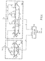
- FIG. 1 is a general block diagram of a digital signal processor in accordance with the invention.
- the entire signal processor is accommodated on a single substrate surface; this can be achieved by means of a known technique.
- the construction as an integrated circuit becomes apparent at the system level by the choice of data input/output mechanisms regarding the environment.
- the processor is especially designed for the high-speed execution of algorithms, particularly those used for digital audio signals.
- a large part of the sub-systems is grouped around the data bus 74 which in this case has a width of 24 bits. Data can be exchanged notably bidirectionally with the environment via input/output member 38 which comprises a byte-organized (de)-multiplexer and which will be described in detail hereinafter.
- serial input member 34 which comprises two connections SDI 1, 2 having a width of 1 data bit
- serial output member 36 which comprises two connections SDO 1, 2 which also have a width of 1 data bit. Control connections have been omitted for the sake of clarity. Several data processors of this kind can thus exchange data.
- the elements 34, 36 also comprise a (de)multiplexer structure for adapting the bit serial connections to the data bus 74 having a width of 24 bits.
- the data received is temporarily stored in a random access read/write memory 32. Intermediate data from the processing elements to be described hereinafter or final results awaiting output to further parts of a system can also be stored therein.
- the memory 32 has a capacity of 64 words of 24 bits each.
- the addresses are supplied by an address selection unit 30 which comprises an address input for receiving an address having a width of 6 bits, and an increment input having a width of 1 bit.
- the addresses and increment signals are supplied by the program memory 66 to be described in detail hereinafter.
- the addresses received are added to the count value in an address counter for a preset address, said counter being included in the address selector.
- theaddress selector 30 also comprises a full adder having a width of 6 bits.
- the mode control signals for the address selector and the six-bit relative addresses are also supplied by the program memory 66.
- the data stored in the memory 32 can be delayed as it were by incrementation and decrementation in order to be inserted in various positions in the formulae of the operations to be executed. Successive operations can thus produce a time sequence of result quantities. Because of this it is not necessary to shift data to and from in the memory 32.
- the data Prior to processing, the data can be stored in one of the registers 44, 46, each of which has a capacity of 24 bits.
- the load control signal is shown separately.
- the register Y is connected to a 24-bit wide input of the multiplier element 48.
- An example of such an element is described in Patent Application GB 2,030,743 and the corresponding US Patent Application Serial No. 228,887 (PHN 9223).
- the h-register 44 can apply, as desired,the 12-most-significant or the 12 least-significant data bits to the multiplier element 48 via a 12-bit wide intermediate bus 78. This bus is proportioned notably in accordance with the length of the coefficients to be supplied by the coefficient memory 58.
- This memory comprises two memory banks for a foreground page and a background page, respectively.
- Each bank has a capacity of 64 12-bit words.
- the coefficient memory can be addressed in two ways: first of all by means of a 6-bit address which is derived from a microcode word read from the memory 66.
- the addresses can also be supplied via the series parallel converter 62 which is fed by the control bus 76.
- This bus is connected to the environment via the interface unit 72.
- the latter is externally connected to an external bus of the I 2 C-type described in European Patent Application 81201168.2 (PHN 9873).
- PPN 9873 European Patent Application 81201168.2
- the latter is used notably if, for example, the nature of the data changes due to changing circumstances; this nature concerns, for example, the characteristics of the audio data.
- the external I 2 C connection is not shown separately.
- the external bus supplies 8-bit bytes which are operative for the memory 60, notably for the background page thereof (the upper half in the Figure).
- the first byte forms a start address: two of the 8 bits are ignored.
- the second byte forms the first part of the first data word (8 bits).
- the third byte forms the second part of the first data word (4 bits) plus the first part of the second data word (4 bits).
- the fourth byte forms the second part of the second data word (8 bits), the series being continued thus until the data source also supplies a termination signal.
- the addresses in the memory 60 are incremented for each new data word until an external new address is input. This input takes place in the background page of the memory 60.
- the double switch 61 then occupies its lower position, so that the foreground page supplies information (addressed by the program memory) for the register 58.
- the foreground page and the background page are then addressed separately; the necessary read (foreground) and write (background) control signals are not shown separately.
- a termination signal of a series of updating operations initiates the copying of the updated data onto the foreground page (if necessary).
- This terminal signal is supplied for example by a host computer.
- the internally synchronized transfer then takes place as follows.
- the double switch 61 is set to its upper position; the foreground page and the background page are then addressed simultaneously, read operations then taking place in the background page and write operations in the foreground page. The functions of foreground page and background page are thus actually temporarily interchanged.
- the switch 61 is switched over again and a subsequent updating operation may commence.
- For each address read one twelve-bit coefficient is stored in the register 58.
- the multiplier element 48 multiplies a quantity having a width of 24 bits, and outputs a product having a width of 36 bits.
- the output of the multiplier element 48 is connected to one input of the arithmetic and logic unit (ALU) 50.
- ALU arithmetic and logic unit
- the output of the ALU 50 is fed-back to an input thereof via a 40-bit accumulator register 54.
- the main task of the ALU 50 is to accumulate the output data of the multiplier element 48; in this respect input multiplexers are suitable units for introducing the correct scale values.
- the rounding off to 24 bits is also performed in the ALU (be it that this requires some processing time).
- the 24-bit result again fits in the register 52.
- the load and hold control signals for this purpose are shown separately.
- the element 56 looks after overflow conditions and clipping operations. These operations will be described in detail with reference to Figure 3.
- a two-bit control bus 76 on which a bus protocol is maintained for transporting the data, organized as 8-bit bytes, between the various elements connected (sometimes also 12-bit symbols).
- One line carries the data; while the second line carries a symbol-wise organized enable signal.
- the bit synchronization is provided by the output signal of a clock, which forms part of the data processor but which is not shown separately, said clock having an output frequency of 6 MHz. This is very high in comparison with the maximum bit frequency of approximately 100 KHz defined in accordance with the 1 2 C protocol.
- the series/parallel converter for data and addresses which is connected to the bus 76 and which serves the coefficient memory 60 has already been discussed.
- a monitor element 40 for monitoring the transport on the data bus 74; under the control of the signal CLM, a data wort transport can be detected each time, for example by means of a bit-wise OR- operation over the full width of the data path.
- the detection result can be applied as an activation signal to a host computer which is connected to the interface element 72 via said I 2 C-bus. Otherwise, this connection serves mainly for applying data to the data processor of Figure 1).
- a second series/parallel converter 70 for converting data which is received serially via the interface unit 72 and which is transported on the bus 76 into parallel 8-bit address words in order to load the program counter 68.
- the latter receives a load control signal LD and counts at the aforesaid frequency of 6 MHz under the control of the aforementioned local clock signals.
- the signal CL acts as an enable signal; in given circumstances it will be necessary to halt the operation of the program counter 68 for some time.
- the program memory 66 has a capacity of 192 words of 35 bits each (this word length, of course, is chosen as desired).
- the program words control the control logic (not shown) of the data path, and further elements of the circuit such as an address selector 30, the read/write memory 60, various registers and selectors, processing elements (48, 50); the microcode output " / uC" is indicated symbolically.
- the code does not comprise a branch facility, so that incrementation can be continued until a new address is loaded.
- the synchronization signals are supplied by the element 64 under the control of external clock signals of 22 kHz, 44 kHz and 88 kHz and a two-bit frequency selection signal from the memory 66. The external frequencies are determined by the use for audio signals.
- the program can be changed by means of an updated set of coefficients in the memory 60.
- the element 64 also receives the signal having the local clock frequency (6 MHz).
- Some (f the operations in a data processor of this kind may be, for example:
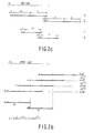
- Figure 2a symbolically shows the structure for data (d) and coefficients (c).
- the heavy lines indicate a bit series; the most significant bit is shown at the left in the Figure.
- the thin lines indicate the number of bits.
- the quantities are defined in the two's-complement notation.
- the most-significant part(d) of the data consists of 24 bits, including the conventional sign bit.
- the least significant part of the data (d) consists of 24 bits, the most-significant bits being void and having the values "00".
- the most-significant part of the coefficients (c) consists of 12 bits, including the conventional sign bit.
- the least-significant part (c) of the coefficients consists of 12 bits, the (single) most-significant bit being void and having the value "O".
- the multi-precision quantities must then be stored in several address locations of the relevant memories. If necessary, less-significant parts of a data quantity are supplemented by dummy bits.
- the first line represents the multiplication of the two least-significant parts (c) and (d).
- the shifting is indicated in the Figure in that the newly formed product is positioned a distance of 11 bits more to the left.
- This operation is subsequently executed for the products (c)x(d) and (c)x(d).
- the result is available with more than double the data precision as shown at the bottom in the Figure.
- the least-significant operations are thus performed first. It is to be noted that within the operations for one data word this has consequences as regards the memory 32, because the element 38 receives the data values with the most-significant parts first.
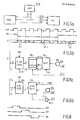
- the facilities required for shifting will be described with reference to Figure 3.
- results are stored as follows: after the third multiplication (including accumulation), the 11 least-significant bits are applied to register 114 in Figure 3. After the fourth multiplication (including accumulation), the 11 least-significant bits are transferred from the register 114 to the register 116, the elevent bits of next-higher significance are transferred to the register 114, and the most-significant part is transferred to the reg _ ster 112.
- FIG. 3 shows a more detailed organization of the registers on the basis of Figure 1. Corresponding parts are denoted by the same reference numerals. The numbering of the bit positions is also shown.
- the data bus 74 is connected to the X-register 44 via a selector 100.
- the signal MS/LS causes the 12 most/leas significant bits to be conducted to the register 44 alternately. Bit 11 of the least-significant half is given the value "O" in accordance with the coefficient convention of Figure 2a.
- Coefficient bus 78 is now replaced by a selector 102.
- Element 42 conducts the most-significant bit (No. 23) from the data bus under the control of the signal CLS. This is supplemented by a "1" in the bit position 10 and for the remainder by ten "zero" bits.
- the data is applied from the element 58 to relevant inputs of the selector 102 in non-inverted form as well as in inverted form via the element 59.
- the signal SELX (2 bits) causes one at the most of the four quantities presented to be conducted to the multiplier 48: either a coefficient, or half an operand, or a sign bit.
- the multiplier 48 outputs a product in two's-complement notation to the selector 106.
- the 40-bit adder 108 is connected to the selector 104.
- the 24 most-significant bits are stored in the register 112.
- the bits 39 ... 45 are overflow bits.
- the eleven least-significant bits of the result from ALU 50 can be stored in the register 114 which also comprises a slave register 116 for 11 bits also.
- the registers 114, 116 can together present, with suppletion of two most-significant "zero" -bits, a 24-bit operand to the selector 118.
- This selector also receives an operand (01111 .. which is decimal + 0.99) and an operand 1000 (which is decimal -1).
- ENRES Under the control of a two-bit signal ENRES, only one of the four quantities is applied to the data bus 74.
- the registers 114, 116 allow for a multi-precision operation.
- the bits 23, 22 for the extreme right part of the selector 118 are the "zero" dummy bits described earlier.
- the power part (elements 110, 118) of this Figure is a detailed representation of the elements 52, 56 in Figure 1.
- the selector 106 is fed by the multiplier 48.
- the 36-bit operand can first of all be applied as usual to the part 120, the most-significant bit being copied five times on bits of higher significance; this is the customary "sign extension".
- the operand is also applied to the part 122 with suppletion by a least-significant "0" and copying of the most-significant bit (34) on four bits of higher significance (39 ... 36). This means that the operand is multiplier by "2".
- the operand is also applied to the part 124 with suppletion by five least-significant zeroes. This means that the operand is multiplied by "32".
- Input 128 is connected to the accumulator 54 of Figure 3.
- a two-bit selection signal FR causes one of the four operands received to be conducted to the 40-bit adder 108.
- the selector 104 is fed by the accumulator register 54.
- the 40-bit operand can first of all be applied to the part 132 in the usual manner.
- the 29 most-significant bits of the operand can be applied secondly to the part 134, the most significant bit (39) being copied eleven times on the input bits of higher significance of this selector part. This means that the relevant operand is multiplied by 1/2048 (2-11).
- the part 130 receives an operand which consists entirely of "0" bits.
- a two-bit selection signal FL causes only one of the three quantities received to be conducted to the adder unit 108.
- Serial and parallel-operating connection units are provided for the exchange of data with inter alia other digital signal processors, D/A and A/D converters, an external memory and a host microprocessor.
- connection elements comprise synchronization means which are activated by the relevant clock.
- Figure 5a shows the relevant sub-stations: the transmitting station is shown at the left and the receiving station is shown at the right; the control station is shown at the top.
- Figure 5b shows the appropriate synchronization protocol.
- the data is despatched with the most-significant bit in front.
- the synchronization signal SCK synchronizes the bits in this sequence.
- the transitions in the synchronization signal WS always occur at the beginning of the least-significant bit of a multibit word. Thanks to this configuration, the precision of an audio data entity received need not be known in advance at the receiver, because it is informed of the precision by the signal WS.
- Figures 6a, 6b show a facility for one of the serial input connections for performing a conversion between external and internal data signals.
- the format of the external data signals in series representation may have a maximum length of 24 bits.
- Figure 6a concerns the input.
- the parts 74, 148 have already been described.
- the input synchronization is provided by an AND-gate 180.
- the shift register 184 serves for alignment and, under the control of the clock pulses from the gate 180, it stores a "1" which is followed exclusively by zeroes.
- the output signals of the shift register on the parallel output thus contain a single “1” and 23 “0" bits, the 1 being shifted through one position in reaction to each clock pulse.
- the output signal of the shift register 184 serves as a write control signal (address) for a 24 x 1 bit memory 186 which receives the data SDI.
- Figure 6b concerns the output.
- the trigger register 204 receives the bits in parallel. Subsequently, they are transported to the shift register 210 under the control of a load signal STRO. The shifting out of the series of bits is controlled by the output signal of the AND-gate 212 which receives the signals SCK and SOEN.
- Figure 7 shows the organization of the parallel- wise data communication with the environment which has already been briefly described with reference to the element 38 in Figure 1. Corresponding elements are denoted by the same reference numerals.
- the external bus 300 having a width of 8 bits, is connected to the selector 301 and to the register 302.
- the selector 301 conducts the bit position 0...3 or the bit positions 4...7 to the register 302 under the control of the signal SDIN4.
- the register 302 has a width of 24 bits, like the bus 74. It receives a load control signal PCK and a six-bit selection signal SELDAT. For this six-bit signal an arbitrary selection from the six four-bit sections of the register 302 can be made (many combinations are not used in practice).
- the register 302 can thus be filled with the data bytes from the bus 300 in three steps. Using the selector 301, one half byte can also be written in the bit positions 0...3 in an arbitrary register section. When the register 302 contains an adequate amount of data, the latter is transferred to the 24-bit register 304. The synchronization "inside" the data processor is thus uncoupled from the synchronization "outside".
- the register 304 also receives a load control signal DENP, a clock signal CL having the afore-said internal 6 MHz frequency, and an enable signal ENDAT for controlling the tristate buffer of this register.
- the register 306 receives a load control signal DCPP and a 6 MHz clock signal CL.
- the register 308 receives a take- over control signal CPDAT.
- the output of the register 308 is connected to a selector 310 in order to apply one of the three butes to the data bus 300.
- a second selector 312 forms the counterpart of the selector 301 in order to enable each half byte to be applied as desired from the register 308 to the bit positions 0...3 of the bus 300.
- This bus can thus be used for two half bytes; the bus then acts as a source for one half byte and as a destination for the other half byte. Further facilities are provided for the processing of addresses.
- the addresses have a length of 16 bits and appear on a predetermined selection of 16 bus lines in the bus 74.
- Theregisters 314 and 316 correspond to the registers 306, 308 and have their own load control signals and a 16-bit capacity.
- the selector 318 transfers one of the two address bytes under the control of a signal SELADO (1 bit).
- the address adder 320 is capable of adding two eight-bit addresses/address portions, starting with the least-significant address portion. Its counterpart is then stored in the two eight-bit registers 322, 324, so that an address-accumulator is formed; a special aspect is that the accumulator registers are thus connected in series.
- Any carry signal from the least-significant address portion is temporarily stored in the bit stage 326 which is fed back, via a selector 328, to the carry input of the adder 320. Also shown are a load control signal CKAD, erase control signals CLEAR, and a selection signal SELCAR which actually serves to ignore the carry signal because the second input of the selector 328 receives a signal.
- This address-forming organization is chosen notably to enable a dynamic read/write memory RAM to be connected.
- Figure 8 shows the time sequence of timing signals required for this purpose. The upper line shows the row address selection signal RAS. At the end of the pulse, the row address for the memory must be known.
- the second line shows the column address selection signal CAS.
- the column address for the memory must be known at the end of the pulse.
- the third line shows the write control signal WE.
- the data of the memory becomes available for a user.
- data supplied by a data source is written in the memory.
- the memories may be of a conventional type.: For the host processor use can be made of, for example, a microcomputer 8048 manufactured by VALVO.
Landscapes
- Engineering & Computer Science (AREA)
- Theoretical Computer Science (AREA)
- Physics & Mathematics (AREA)
- General Physics & Mathematics (AREA)
- General Engineering & Computer Science (AREA)
- Computational Mathematics (AREA)
- Computing Systems (AREA)
- Mathematical Analysis (AREA)
- Mathematical Optimization (AREA)
- Pure & Applied Mathematics (AREA)
- Software Systems (AREA)
- Complex Calculations (AREA)
Applications Claiming Priority (2)
| Application Number | Priority Date | Filing Date | Title |
|---|---|---|---|
| NL8304186 | 1983-12-06 | ||
| NL8304186A NL8304186A (nl) | 1983-12-06 | 1983-12-06 | Geintegreerde processor voor het verwerken van woordsgewijze ontvangbare informatie. |
Publications (2)
| Publication Number | Publication Date |
|---|---|
| EP0146984A1 true EP0146984A1 (de) | 1985-07-03 |
| EP0146984B1 EP0146984B1 (de) | 1990-01-31 |
Family
ID=19842838
Family Applications (1)
| Application Number | Title | Priority Date | Filing Date |
|---|---|---|---|
| EP84201725A Expired EP0146984B1 (de) | 1983-12-06 | 1984-11-28 | Prozessor für die Verarbeitung von Wort für Wort empfangbaren Daten |
Country Status (6)
| Country | Link |
|---|---|
| US (1) | US4627021A (de) |
| EP (1) | EP0146984B1 (de) |
| JP (1) | JPS60140463A (de) |
| KR (1) | KR920010914B1 (de) |
| DE (1) | DE3481234D1 (de) |
| NL (1) | NL8304186A (de) |
Families Citing this family (28)
| Publication number | Priority date | Publication date | Assignee | Title |
|---|---|---|---|---|
| US5201029A (en) * | 1988-10-24 | 1993-04-06 | U.S. Philips Corporation | Digital data processing apparatus using daisy chain control |
| US5214767A (en) * | 1989-02-07 | 1993-05-25 | Compaq Computer Corp. | Full address and odd boundary direct memory access controller which determines address size by counting the input address bytes |
| US5204962A (en) * | 1989-11-30 | 1993-04-20 | Mitsubishi Denki Kabushiki Kaisha | Processor with preceding operation circuit connected to output of data register |
| JP3231429B2 (ja) * | 1992-11-06 | 2001-11-19 | 株式会社日立製作所 | 中央処理装置と乗算器とを有する半導体集積回路装置 |
| JP2784440B2 (ja) * | 1993-04-14 | 1998-08-06 | インターナショナル・ビジネス・マシーンズ・コーポレイション | データ・ページの転送制御方法 |
| US6131108A (en) * | 1998-03-31 | 2000-10-10 | Lsi Logic Corporation | Apparatus, and associated method, for generating multi-bit length sequences |
| US7242912B2 (en) | 1998-05-29 | 2007-07-10 | Silicon Laboratories Inc. | Partitioning of radio-frequency apparatus |
| US7024221B2 (en) * | 2001-01-12 | 2006-04-04 | Silicon Laboratories Inc. | Notch filter for DC offset reduction in radio-frequency apparatus and associated methods |
| US6970717B2 (en) | 2001-01-12 | 2005-11-29 | Silicon Laboratories Inc. | Digital architecture for radio-frequency apparatus and associated methods |
| US7035607B2 (en) | 1998-05-29 | 2006-04-25 | Silicon Laboratories Inc. | Systems and methods for providing an adjustable reference signal to RF circuitry |
| US7228109B2 (en) * | 2001-01-12 | 2007-06-05 | Silicon Laboratories Inc. | DC offset reduction in radio-frequency apparatus and associated methods |
| US7221921B2 (en) | 1998-05-29 | 2007-05-22 | Silicon Laboratories | Partitioning of radio-frequency apparatus |
| US7092675B2 (en) | 1998-05-29 | 2006-08-15 | Silicon Laboratories | Apparatus and methods for generating radio frequencies in communication circuitry using multiple control signals |
| US6804497B2 (en) * | 2001-01-12 | 2004-10-12 | Silicon Laboratories, Inc. | Partitioned radio-frequency apparatus and associated methods |
| US6993314B2 (en) | 1998-05-29 | 2006-01-31 | Silicon Laboratories Inc. | Apparatus for generating multiple radio frequencies in communication circuitry and associated methods |
| US6484194B1 (en) | 1998-06-17 | 2002-11-19 | Texas Instruments Incorporated | Low cost multiplier block with chain capability |
| JP2000039995A (ja) * | 1998-06-25 | 2000-02-08 | Texas Instr Inc <Ti> | 高性能マイクロプロセッサで使用するためのフレキシブル累算レジスタファイル |
| EP0967543B1 (de) * | 1998-06-25 | 2004-09-29 | Texas Instruments Incorporated | Verfahren zum Multiplizieren von Zahlen in Mehrwortkettendarstellung |
| US6903617B2 (en) | 2000-05-25 | 2005-06-07 | Silicon Laboratories Inc. | Method and apparatus for synthesizing high-frequency signals for wireless communications |
| KR100457040B1 (ko) * | 2000-06-21 | 2004-11-10 | 패러데이 테크놀로지 코퍼레이션 | 곱셈 누산 명령을 이용한 데이터 처리 장치 및 방법 |
| US7138858B2 (en) | 2001-01-12 | 2006-11-21 | Silicon Laboratories, Inc. | Apparatus and methods for output buffer circuitry with constant output power in radio-frequency circuitry |
| US20030232613A1 (en) * | 2001-01-12 | 2003-12-18 | Kerth Donald A. | Quadrature signal generation in radio-frequency apparatus and associated methods |
| US7177610B2 (en) * | 2001-01-12 | 2007-02-13 | Silicon Laboratories Inc. | Calibrated low-noise current and voltage references and associated methods |
| US7158574B2 (en) * | 2001-01-12 | 2007-01-02 | Silicon Laboratories Inc. | Digital interface in radio-frequency apparatus and associated methods |
| US7031683B2 (en) * | 2001-01-12 | 2006-04-18 | Silicon Laboratories Inc. | Apparatus and methods for calibrating signal-processing circuitry |
| US7035611B2 (en) * | 2001-01-12 | 2006-04-25 | Silicon Laboratories Inc. | Apparatus and method for front-end circuitry in radio-frequency apparatus |
| EP1486079B1 (de) * | 2002-03-15 | 2015-12-30 | Silicon Laboratories Inc. | Hochfrequenzvorrichtung |
| US7370167B2 (en) * | 2003-07-17 | 2008-05-06 | Sun Microsystems, Inc. | Time slicing device for shared resources and method for operating the same |
Citations (2)
| Publication number | Priority date | Publication date | Assignee | Title |
|---|---|---|---|---|
| EP0051422A2 (de) * | 1980-10-31 | 1982-05-12 | Hitachi, Ltd. | Hochgeschwindigkeitsdigitalprozessor |
| GB2115588A (en) * | 1982-02-19 | 1983-09-07 | Sony Corp | Digital signal processing systems |
Family Cites Families (4)
| Publication number | Priority date | Publication date | Assignee | Title |
|---|---|---|---|---|
| US4130879A (en) * | 1977-07-15 | 1978-12-19 | Honeywell Information Systems Inc. | Apparatus for performing floating point arithmetic operations using submultiple storage |
| US4238833A (en) * | 1979-03-28 | 1980-12-09 | Monolithic Memories, Inc. | High-speed digital bus-organized multiplier/divider system |
| JPS57212542A (en) * | 1981-06-24 | 1982-12-27 | Toshiba Corp | Multiplying circuit |
| JPS58144259A (ja) * | 1982-02-19 | 1983-08-27 | Sony Corp | デイジタル信号処理装置 |
-
1983
- 1983-12-06 NL NL8304186A patent/NL8304186A/nl not_active Application Discontinuation
-
1984
- 1984-03-13 US US06/589,243 patent/US4627021A/en not_active Expired - Lifetime
- 1984-11-28 DE DE8484201725T patent/DE3481234D1/de not_active Expired - Lifetime
- 1984-11-28 EP EP84201725A patent/EP0146984B1/de not_active Expired
- 1984-12-05 KR KR1019840007673A patent/KR920010914B1/ko not_active Expired
- 1984-12-06 JP JP59258395A patent/JPS60140463A/ja active Pending
Patent Citations (2)
| Publication number | Priority date | Publication date | Assignee | Title |
|---|---|---|---|---|
| EP0051422A2 (de) * | 1980-10-31 | 1982-05-12 | Hitachi, Ltd. | Hochgeschwindigkeitsdigitalprozessor |
| GB2115588A (en) * | 1982-02-19 | 1983-09-07 | Sony Corp | Digital signal processing systems |
Non-Patent Citations (2)
| Title |
|---|
| ICASSP 82 PROCEEDINGS CONFERENCE, Paris, 3rd-5th May 1982, vol. 2, pages 1061-1064, IEEE, New York, US; D. KARLIN: "VLSI building blocks for digital signal processing" * |
| IEEE TRANSACTIONS ON COMPUTERS, vol. C-23, no. 8, August 1974, pages 808-817, New York, US; G.L. KRATZ et al.: "A microprogrammed approach to signal processing" * |
Also Published As
| Publication number | Publication date |
|---|---|
| JPS60140463A (ja) | 1985-07-25 |
| EP0146984B1 (de) | 1990-01-31 |
| US4627021A (en) | 1986-12-02 |
| KR920010914B1 (ko) | 1992-12-24 |
| NL8304186A (nl) | 1985-07-01 |
| DE3481234D1 (de) | 1990-03-08 |
| KR850004679A (ko) | 1985-07-25 |
Similar Documents
| Publication | Publication Date | Title |
|---|---|---|
| EP0146984B1 (de) | Prozessor für die Verarbeitung von Wort für Wort empfangbaren Daten | |
| EP1176718B1 (de) | Hardware-Beschleuniger für eine auf Basis einer geringsten quadratischen Mittelwert-Algorithmus Koeffizientenanpassung | |
| US5297071A (en) | Arithmetic circuit, and adaptive filter and echo canceler using it | |
| KR100310584B1 (ko) | 승산-가산연산을이용한신호처리시스템 | |
| US5103416A (en) | Programmable digital filter | |
| US5457805A (en) | Microcomputer enabling high speed execution of product-sum operation | |
| US4796217A (en) | Rounding unit for use in arithmetic processing of floating point data | |
| JPH07112144B2 (ja) | デジタル・フィルタ | |
| JPH082014B2 (ja) | 多段デジタル・フィルタ | |
| US3914588A (en) | Digital filters | |
| US5164724A (en) | Data format converters for use with digit-serial signals | |
| US5402368A (en) | Computing unit and digital signal processor using the same | |
| US5944775A (en) | Sum-of-products arithmetic unit | |
| US6108681A (en) | System for sharing resources in a digital filter | |
| US5781462A (en) | Multiplier circuitry with improved storage and transfer of booth control coefficients | |
| US5602766A (en) | Method of and device for forming the sum of a chain of products | |
| US5870322A (en) | Multiplier to selectively perform unsigned magnitude multiplication or signed magnitude multiplication | |
| US5499202A (en) | Residue circuit | |
| US5650952A (en) | Circuit arrangement for forming the sum of products | |
| JP2000183753A (ja) | 信号変換装置及び信号変換方法 | |
| JPS58151644A (ja) | デイジタル演算装置 | |
| US4970675A (en) | Multiplier for binary numbers comprising a very high number of bits | |
| JP3850150B2 (ja) | デジタル信号処理動作を実行する方法およびデジタル信号プロセッサ | |
| KR19990063481A (ko) | 필터에서의 계수 사용을 위한 멀티포트 레지스터파일 | |
| JPH1063641A (ja) | シフト付き積和回路 |
Legal Events
| Date | Code | Title | Description |
|---|---|---|---|
| PUAI | Public reference made under article 153(3) epc to a published international application that has entered the european phase |
Free format text: ORIGINAL CODE: 0009012 |
|
| AK | Designated contracting states |
Designated state(s): DE FR GB IT SE |
|
| 17P | Request for examination filed |
Effective date: 19851220 |
|
| 17Q | First examination report despatched |
Effective date: 19870730 |
|
| GRAA | (expected) grant |
Free format text: ORIGINAL CODE: 0009210 |
|
| AK | Designated contracting states |
Kind code of ref document: B1 Designated state(s): DE FR GB IT SE |
|
| REF | Corresponds to: |
Ref document number: 3481234 Country of ref document: DE Date of ref document: 19900308 |
|
| ITF | It: translation for a ep patent filed | ||
| ET | Fr: translation filed | ||
| PLBE | No opposition filed within time limit |
Free format text: ORIGINAL CODE: 0009261 |
|
| STAA | Information on the status of an ep patent application or granted ep patent |
Free format text: STATUS: NO OPPOSITION FILED WITHIN TIME LIMIT |
|
| 26N | No opposition filed | ||
| PGFP | Annual fee paid to national office [announced via postgrant information from national office to epo] |
Ref country code: GB Payment date: 19921105 Year of fee payment: 9 |
|
| PGFP | Annual fee paid to national office [announced via postgrant information from national office to epo] |
Ref country code: FR Payment date: 19921120 Year of fee payment: 9 |
|
| PGFP | Annual fee paid to national office [announced via postgrant information from national office to epo] |
Ref country code: SE Payment date: 19921126 Year of fee payment: 9 |
|
| ITTA | It: last paid annual fee | ||
| PGFP | Annual fee paid to national office [announced via postgrant information from national office to epo] |
Ref country code: DE Payment date: 19930128 Year of fee payment: 9 |
|
| PG25 | Lapsed in a contracting state [announced via postgrant information from national office to epo] |
Ref country code: GB Effective date: 19931128 |
|
| PG25 | Lapsed in a contracting state [announced via postgrant information from national office to epo] |
Ref country code: SE Effective date: 19931129 |
|
| GBPC | Gb: european patent ceased through non-payment of renewal fee |
Effective date: 19931128 |
|
| PG25 | Lapsed in a contracting state [announced via postgrant information from national office to epo] |
Ref country code: FR Effective date: 19940729 |
|
| PG25 | Lapsed in a contracting state [announced via postgrant information from national office to epo] |
Ref country code: DE Effective date: 19940802 |
|
| REG | Reference to a national code |
Ref country code: FR Ref legal event code: ST |
|
| EUG | Se: european patent has lapsed |
Ref document number: 84201725.3 Effective date: 19940610 |