EP0146966A2 - Verbundrechnersystem - Google Patents
Verbundrechnersystem Download PDFInfo
- Publication number
- EP0146966A2 EP0146966A2 EP84116339A EP84116339A EP0146966A2 EP 0146966 A2 EP0146966 A2 EP 0146966A2 EP 84116339 A EP84116339 A EP 84116339A EP 84116339 A EP84116339 A EP 84116339A EP 0146966 A2 EP0146966 A2 EP 0146966A2
- Authority
- EP
- European Patent Office
- Prior art keywords
- transmission lines
- data
- looped
- computer system
- processors
- Prior art date
- Legal status (The legal status is an assumption and is not a legal conclusion. Google has not performed a legal analysis and makes no representation as to the accuracy of the status listed.)
- Granted
Links
Images


Classifications
-
- G—PHYSICS
- G06—COMPUTING OR CALCULATING; COUNTING
- G06F—ELECTRIC DIGITAL DATA PROCESSING
- G06F15/00—Digital computers in general; Data processing equipment in general
- G06F15/76—Architectures of general purpose stored program computers
- G06F15/80—Architectures of general purpose stored program computers comprising an array of processing units with common control, e.g. single instruction multiple data processors
- G06F15/8007—Architectures of general purpose stored program computers comprising an array of processing units with common control, e.g. single instruction multiple data processors single instruction multiple data [SIMD] multiprocessors
- G06F15/8023—Two dimensional arrays, e.g. mesh, torus
-
- H—ELECTRICITY
- H04—ELECTRIC COMMUNICATION TECHNIQUE
- H04L—TRANSMISSION OF DIGITAL INFORMATION, e.g. TELEGRAPHIC COMMUNICATION
- H04L12/00—Data switching networks
- H04L12/28—Data switching networks characterised by path configuration, e.g. LAN [Local Area Networks] or WAN [Wide Area Networks]
- H04L12/46—Interconnection of networks
- H04L12/4637—Interconnected ring systems
Definitions
- the present invention relates to a combination of processors that have a uniform transmission pro- c essing function, and more specifically to a combined computer system that is constituted in a one-dimensional to three-dimensional manner.
- Network systems for connecting a plurality of processors have heretofore been either a bus structure, a loop structure, a star structure, or a mesh structure.
- the first three of these structures can not be constructed in a three-dimensional configuration.
- routing is complex.
- the processor at the center of the structure is different from the other processors.
- a particular processor In a mesh structure, a particular processor must work to cope with any change in the structure of the system or with any abnormal condition that may occur, thereby making it difficult to expand and maintain the system.
- the present invention provides a method for constituting processors that serve as constituent units of a system in which very uniform constituent units are connected through a plurality of looped transmission lines, which can be constructed in two-dimensional and three-dimensional configurations, and to which a simply constructed transmission system can be adapted.
- the present invention deals with a structure which comprises a first group of looped transmission lines consisting of a plurality of looped transmission lines, a second group of looped transmission lines that consist of at least one looped transmission line and that are arranged to intersect said first group of looped transmission lines, transmission lines that couple said intersecting transmission lines together, and data processing and controlling means that control the transmission of data along the transmission lines and that process the data, and wherein, as required, the number of building blocks is increased or decreased for each of the looped transmission lines.
- Fig. 1 is a diagram of constituent units according to the present invention
- Figs. 2 to 13 are diagrams showing a plurality of processors that are connected in the form of networks according to the present invention
- Fig. 14 is a diagram of a data processing and controlling unit according to the present invention.
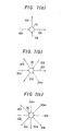
- Fig. 1 shows three kinds of constituent elements (a), (b) and (c) that will be combined in the form of building blocks to constitute a system.
- the constituent unit consists of a processor and unidirectional transmission lines for transmitting the data therefrom to other processors. Transmission lines of neighboring processors are connected to the unidirectional transmission lines so as to form pairs and so as to receive the data therefrom.
- Diagrams (a), (b) and (c) of-Fig. 1 illustrate constituent units that consist of processors 10, 20 and 30, and two, three and four transmission lines (101, 102), (201, 202, 203), and (301, 302, 303, 304), respectively.
- transmission lines 101, 102, 201, 202, 203, 301, 302, 303 and 304 are connected transmission lines 10k, 10i, 20k, 20l, 20m, 30k, 30l, 30m and 30n of the neighboring processors to form pairs.
- Figs. 2 to 13 show transmission lines of the processors forming pairs, that are connected successively.
- the constituent units are all the same, hence, each of the transmission lines constitutes a portion of a closed loop transmission line.
- the constituent unit may have any number of unidirectional transmission lines in addition to the above-mentioned numbers.
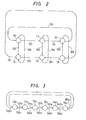
- Figs. 2 to 5 illustrate examples of connecting the constituent units that have two unidirectional transmission lines.
- Fig. 2 illustrates an example in which the processors are divided into two groups consisting of (10, 11, 12) and (13, 14, 15) which are coupled through a loop (101, 111, 121) and a loop (131, 151, 141).
- the processors (10, 13), (11, 14) and (12, 15) on these different loops are coupled via a loop (102, 132), a loop (112, 142) and a loop (122, 152).
- Fig. 3 shows an example in which all of the processors are coupled through the same loops.
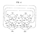
- Fig. 4 illustrates an example in which the processors are divided into three groups (10b, 11b, 12b, 13b), (14b, 15b, 16b, 17b) and (18b, 19b, 20b, 21b) which are coupled in the form of loops. Unlike the example of Fig. 2, however, processors (10b, 11b), (12b, 13b), (18b, 19b) and (20b, 21b) on the same loops are coupled. In this regard, the example of Fig. 4 resembles the example of Fig. 3.
- processors 14b, 15b, 16b, 17b are connected to constitute loops that traverse the above-mentioned three loops (101b to 131b), (141b to 151b) and (181b to 211b).
- Fig. 4 is the same as the connection method of Fig. 2.
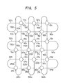
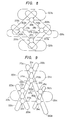
- Fig. 5 shows an example in which processors are divided into three groups (10c, 11c, 12c, 13c, 14c, 15c), (16c, 17c, 18c, 19c, 20c, 21c) and (22c, 23c, 24c, 25c, 26c, 27c) which are coupled in the form of loops.
- the processors 11c, 14c and the processors 23c, 26c exist on the loops (101c to 121c), (221c to 231c) and are not adjacent to each other.
- the processors can be incremented by a unit of one.
- the processors in the arrangement of Fig. 4 can be increased by a unit of six or by a unit of four.
- the processors can be increased by a unit of six processors. Increase in the number of processors changes the structure of system. Therefore, the number of processors to be increased may change thereafter.
- Figs. 6 to 10 illustrate methods for connecting constituent units that have three unidirectional transmission lines.
- the three processors 20, 21 and 22 are connected by loops (202, 212), (211, 221), (203, 223) that connect between the two processors, and by loops 201, 213, 222 of single processors.
- F ig. 8 shows an example in which a processor is added to the structure of Fig. 6.
- Fig. 9 shows an example in which three processors are added to the structure of Fig. 6.
- Fig. 10 illustrates an example in which three processors are added to the structure of Fig. 9. In the structures of Figs. 7 to 10, the processors can be incremented by any integer greater than one.
- Figs. 11 to 13 illustrate methods of connecting constituent units that have four unidirectional transmission lines.
- Fig. 11 shows an example in which nine processors are arranged in a two-dimensional manner
- Fig. 12 shows an example in which three processors are arranged in a one-dimensional configuration
- Fig. 13 shows an example in which 32 processors are arranged in a three-dimensional configuration.
- Fig. 13 is an expansion of the structure of Fig. 11.
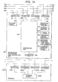
- Fig. 14 shows the internal structure of the constituent units 10, 20 and 30. Responsive to the numbers 2, 3, 4 of unidirectional transmission lines of the constituent units 10, 20 and 30, however, there exist two, three or four interfaces connected to the loop transmission lines.
- the processor consists of a terminal 3000 and a data processing and controlling unit 300 which controls the transmission or reception of information relative to the loop transmission lines.
- the terminal 3000 consists of a terminal device 3005 and interfaces 3001 to 3004 between the terminal device and the data processing and controlling unit.
- the four interfaces 3001 to 3004 make connection with different data processing and controlling units, and may be provided in any number greater than one.
- Described below is a process in which data generated from the terminal device 3005 is transmitted to a predetermined terminal via a loop transmission line.
- Data generated from the terminal device 3005 is sent to data processing and controlling units via interfaces 3001 to 3004.
- Data sent from the terminal device via an interface 322 is then stored in a sending buffer 317.
- Data is provided with an address (receiving address) of a terminal where the data will be received or a code (content code) corresponding to the content of the data.
- a routine table 323 has been written a program which determines in which loop direction the data should be transmitted corresponding to the address or the content code. The program has been written onto the routine table 323 prior to sending the data.
- the operational unit 315 sends that data from any one of the interfaces 311 to 314 relying upon the routine table 323.
- the operational unit 315 judges that the data is properly transmitted, and erases the data from the sending buffer 317.
- the data that is to be sent is provided with an address of the interface that sends the data.
- the address of the interface has been stored beforehand in the ROM of interface address table 321.
- the data processing and controlling unit 300 When data arrives flowing on the loop, the data processing and controlling unit 300 introduces the data through, for example, an interface 311, reads the address of the interface 311 from the interface address table 321, attaches the interface address, and stores the data in a receiving buffer 316. If the data received is not the data that is generated from the data processing and controlling unit 300, the data is then sent through the interface 311 that has received the data. If the data is the data that is generated from the data processing and controlling unit 300, that data is erased from the receiving buffer 316 and from the sending buffer 317 as mentioned above.
- an interface 311 reads the address of the interface 311 from the interface address table 321, attaches the interface address, and stores the data in a receiving buffer 316. If the data received is not the data that is generated from the data processing and controlling unit 300, the data is then sent through the interface 311 that has received the data. If the data is the data that is generated from the data processing and controlling unit 300, that data is erased from the receiving buffer 316 and from
- the operational unit 315 transfers the data to the terminal via the interface 322 provided the receiving address or the content code of the data is in agreement with that of a receiving function code table and address 320.
- the receiving address or the content code of the data is in agreement with that in the routine table 323, said data is sent in the direction of the transmission loop written thereon through interfaces 311 to 314 of directions other than the loop direction in which the data is received.
- the data is erased from the receiving buffer 316.
- the data processing and controlling unit sets the timer 318 for each of the data. If the data does not return even after a predetermined period of time has passed, the data processing and controlling unit sets the flag of an abnormal status register 319 corresponding to the loop into which the data is sent.
- the operational unit 315 broadcasts the abnormal condition on the loop in all directions via the interfaces 311 to 314.
- the data processing and controlling units broadcast the abnormal condition to the loop directions in which the data reporting the abnormal condition has not yet been received.
- the processor which has received the data that reports the abnormal condition converts the routine table 323 corresponding to the abnormal loop. For instance, a by-pass route may have been determined to cope with the abnormal condition that may take place in the loops, or if an abnormal condition develops somewhere, the data may be broadcast in all loop directions thereafter.
- the receiving function code table and address 320 has been stored in advance a content code or an address of the data required by the terminal device 3005 that is connected to the data processing and controlling unit 300.
- the defective portion may be separated to be checked. In this case, transmission of data is continued through other portions. Further, since the constituent units are all the same, maintenance can be easily carried out.
- identical constituent units are successively connected to each other to form a plurality of looped structures.
- a communication network can be constituted that can be easily changed into a one-dimensional, two-dimensional or three-dimensional structure. Further since it is based upon a looped network, transmission routing can be easily accomplished.
- all of the constituent units have the same hardware and software, and no apparatus having particular functions such as a master apparatus is needed, thereby offering an advantage in regard to maintenance.
Landscapes
- Engineering & Computer Science (AREA)
- Computer Hardware Design (AREA)
- Theoretical Computer Science (AREA)
- Computer Networks & Wireless Communication (AREA)
- Signal Processing (AREA)
- Computing Systems (AREA)
- Physics & Mathematics (AREA)
- General Engineering & Computer Science (AREA)
- General Physics & Mathematics (AREA)
- Multi Processors (AREA)
- Data Exchanges In Wide-Area Networks (AREA)
- Small-Scale Networks (AREA)
Applications Claiming Priority (2)
| Application Number | Priority Date | Filing Date | Title |
|---|---|---|---|
| JP246294/83 | 1983-12-28 | ||
| JP58246294A JP2644718B2 (ja) | 1983-12-28 | 1983-12-28 | コンピュータシステム |
Publications (3)
| Publication Number | Publication Date |
|---|---|
| EP0146966A2 true EP0146966A2 (de) | 1985-07-03 |
| EP0146966A3 EP0146966A3 (en) | 1986-09-10 |
| EP0146966B1 EP0146966B1 (de) | 1994-09-07 |
Family
ID=17146407
Family Applications (1)
| Application Number | Title | Priority Date | Filing Date |
|---|---|---|---|
| EP84116339A Expired - Lifetime EP0146966B1 (de) | 1983-12-28 | 1984-12-27 | Verbundrechnersystem |
Country Status (4)
| Country | Link |
|---|---|
| US (1) | US5341504A (de) |
| EP (1) | EP0146966B1 (de) |
| JP (1) | JP2644718B2 (de) |
| DE (1) | DE3486347T2 (de) |
Cited By (4)
| Publication number | Priority date | Publication date | Assignee | Title |
|---|---|---|---|---|
| WO1987002157A1 (en) * | 1985-10-02 | 1987-04-09 | American Telephone & Telegraph Company | Mesh-based switching network |
| EP0293701A3 (en) * | 1987-06-01 | 1990-05-30 | Applied Intelligent Systems, Inc. | Parallel neighborhood processing system and method |
| EP0286240A3 (en) * | 1987-03-11 | 1990-07-25 | Toyo Communication Equipment Co. Ltd. | Computer system |
| US5557734A (en) * | 1994-06-17 | 1996-09-17 | Applied Intelligent Systems, Inc. | Cache burst architecture for parallel processing, such as for image processing |
Families Citing this family (49)
| Publication number | Priority date | Publication date | Assignee | Title |
|---|---|---|---|---|
| JPS62206660A (ja) * | 1986-03-07 | 1987-09-11 | Agency Of Ind Science & Technol | プロセツサ結合装置 |
| JP2743994B2 (ja) * | 1987-06-29 | 1998-04-28 | 株式会社東芝 | 並列処理システム |
| JPH03174648A (ja) * | 1989-09-12 | 1991-07-29 | Nec Corp | 並列処理システム構成集積回路 |
| US6453406B1 (en) * | 1990-10-17 | 2002-09-17 | Compaq Computer Corporation | Multiprocessor system with fiber optic bus interconnect for interprocessor communications |
| US5689719A (en) * | 1991-06-28 | 1997-11-18 | Sanyo Electric O., Ltd. | Parallel computer system including processing elements |
| US5583990A (en) * | 1993-12-10 | 1996-12-10 | Cray Research, Inc. | System for allocating messages between virtual channels to avoid deadlock and to optimize the amount of message traffic on each type of virtual channel |
| US5560027A (en) * | 1993-12-15 | 1996-09-24 | Convex Computer Corporation | Scalable parallel processing systems wherein each hypernode has plural processing modules interconnected by crossbar and each processing module has SCI circuitry for forming multi-dimensional network with other hypernodes |
| US5515510A (en) * | 1994-01-14 | 1996-05-07 | Consilium Overseas Limited | Communications internetwork system connecting a client node array to a resource array |
| US5644714A (en) | 1994-01-14 | 1997-07-01 | Elonex Plc, Ltd. | Video collection and distribution system with interested item notification and download on demand |
| US5701416A (en) * | 1995-04-13 | 1997-12-23 | Cray Research, Inc. | Adaptive routing mechanism for torus interconnection network |
| US5659796A (en) * | 1995-04-13 | 1997-08-19 | Cray Research, Inc. | System for randomly modifying virtual channel allocation and accepting the random modification based on the cost function |
| US6055618A (en) * | 1995-10-31 | 2000-04-25 | Cray Research, Inc. | Virtual maintenance network in multiprocessing system having a non-flow controlled virtual maintenance channel |
| US5864738A (en) * | 1996-03-13 | 1999-01-26 | Cray Research, Inc. | Massively parallel processing system using two data paths: one connecting router circuit to the interconnect network and the other connecting router circuit to I/O controller |
| US5835925A (en) * | 1996-03-13 | 1998-11-10 | Cray Research, Inc. | Using external registers to extend memory reference capabilities of a microprocessor |
| US5898827A (en) * | 1996-09-27 | 1999-04-27 | Hewlett-Packard Co. | Routing methods for a multinode SCI computer system |
| US6101181A (en) * | 1997-11-17 | 2000-08-08 | Cray Research Inc. | Virtual channel assignment in large torus systems |
| US6085303A (en) * | 1997-11-17 | 2000-07-04 | Cray Research, Inc. | Seralized race-free virtual barrier network |
| US6230252B1 (en) | 1997-11-17 | 2001-05-08 | Silicon Graphics, Inc. | Hybrid hypercube/torus architecture |
| US5970232A (en) * | 1997-11-17 | 1999-10-19 | Cray Research, Inc. | Router table lookup mechanism |
| US6314110B1 (en) * | 1998-03-06 | 2001-11-06 | Cisco Technology, Inc. | Method and apparatus for distributed bandwidth allocation for a bi-directional ring media with spatial and local reuse |
| US6216174B1 (en) | 1998-09-29 | 2001-04-10 | Silicon Graphics, Inc. | System and method for fast barrier synchronization |
| US6320501B1 (en) | 1999-05-25 | 2001-11-20 | Pittway Corporation | Multiple sensor system for alarm determination with device-to-device communications |
| US6751698B1 (en) * | 1999-09-29 | 2004-06-15 | Silicon Graphics, Inc. | Multiprocessor node controller circuit and method |
| US6674720B1 (en) | 1999-09-29 | 2004-01-06 | Silicon Graphics, Inc. | Age-based network arbitration system and method |
| CN100385460C (zh) * | 2001-03-13 | 2008-04-30 | 伊强德斯股份有限公司 | 联动式计数器及联动装置 |
| US6783498B2 (en) * | 2002-03-26 | 2004-08-31 | Vivometrics, Inc. | Method and system for extracting cardiac parameters from plethysmographic signals |
| US20040019765A1 (en) * | 2002-07-23 | 2004-01-29 | Klein Robert C. | Pipelined reconfigurable dynamic instruction set processor |
| AU2003252157A1 (en) * | 2002-07-23 | 2004-02-09 | Gatechange Technologies, Inc. | Interconnect structure for electrical devices |
| US20040062196A1 (en) * | 2002-10-01 | 2004-04-01 | Avici Systems, Inc. | Single shelf router |
| TW200416522A (en) | 2003-02-25 | 2004-09-01 | Asustek Comp Inc | Portable computer carrying desktop computer processor and power management method thereof |
| US8307194B1 (en) | 2003-08-18 | 2012-11-06 | Cray Inc. | Relaxed memory consistency model |
| US7543133B1 (en) | 2003-08-18 | 2009-06-02 | Cray Inc. | Latency tolerant distributed shared memory multiprocessor computer |
| US7519771B1 (en) | 2003-08-18 | 2009-04-14 | Cray Inc. | System and method for processing memory instructions using a forced order queue |
| US7366873B1 (en) | 2003-08-18 | 2008-04-29 | Cray, Inc. | Indirectly addressed vector load-operate-store method and apparatus |
| US7421565B1 (en) * | 2003-08-18 | 2008-09-02 | Cray Inc. | Method and apparatus for indirectly addressed vector load-add -store across multi-processors |
| US7503048B1 (en) | 2003-08-18 | 2009-03-10 | Cray Incorporated | Scheduling synchronization of programs running as streams on multiple processors |
| US7735088B1 (en) | 2003-08-18 | 2010-06-08 | Cray Inc. | Scheduling synchronization of programs running as streams on multiple processors |
| US7334110B1 (en) | 2003-08-18 | 2008-02-19 | Cray Inc. | Decoupled scalar/vector computer architecture system and method |
| US7437521B1 (en) | 2003-08-18 | 2008-10-14 | Cray Inc. | Multistream processing memory-and barrier-synchronization method and apparatus |
| US7185138B1 (en) | 2004-05-14 | 2007-02-27 | Peter Galicki | Multi-dimensional data routing fabric |
| US7478769B1 (en) | 2005-03-09 | 2009-01-20 | Cray Inc. | Method and apparatus for cooling electronic components |
| US7380102B2 (en) * | 2005-09-27 | 2008-05-27 | International Business Machines Corporation | Communication link control among inter-coupled multiple processing units in a node to respective units in another node for request broadcasting and combined response |
| TW200712898A (en) * | 2005-09-30 | 2007-04-01 | Tyan Computer Corp | Multi-processor module |
| US7818388B2 (en) * | 2005-10-07 | 2010-10-19 | International Business Machines Corporation | Data processing system, method and interconnect fabric supporting multiple planes of processing nodes |
| US8441942B1 (en) * | 2008-12-03 | 2013-05-14 | Tellabs Operations Inc. | Method and apparatus for link level loop detection |
| JP6946955B2 (ja) * | 2017-11-10 | 2021-10-13 | 富士通株式会社 | 情報処理装置、演算処理装置及び情報処理装置の制御方法 |
| GB201904266D0 (en) * | 2019-03-27 | 2019-05-08 | Graphcore Ltd | A networked computer with embedded rings |
| GB201904267D0 (en) * | 2019-03-27 | 2019-05-08 | Graphcore Ltd | A networked computer with multiple embedded rings |
| CN113424198B (zh) | 2019-11-15 | 2023-08-29 | 昆仑芯(北京)科技有限公司 | 基于柔性电缆连接的分布式ai训练拓扑 |
Family Cites Families (29)
| Publication number | Priority date | Publication date | Assignee | Title |
|---|---|---|---|---|
| US3473160A (en) * | 1966-10-10 | 1969-10-14 | Stanford Research Inst | Electronically controlled microelectronic cellular logic array |
| US3731002A (en) * | 1970-10-08 | 1973-05-01 | Bell Telephone Labor Inc | Interconnected loop data block transmission system |
| JPS5015521A (de) * | 1973-06-08 | 1975-02-19 | ||
| CH584492A5 (de) * | 1974-12-10 | 1977-01-31 | Hasler Ag | |
| JPS51138360A (en) * | 1975-05-26 | 1976-11-29 | Hitachi Ltd | Intra-premiss information control and transmission system |
| JPS5248416A (en) * | 1975-07-23 | 1977-04-18 | Johnson Controls Inc | Data communication system |
| US4177514A (en) * | 1976-11-12 | 1979-12-04 | General Electric Company | Graph architecture information processing system |
| JPS5439503A (en) * | 1977-09-05 | 1979-03-27 | Hitachi Ltd | Priority selection system in ring transmission line |
| US4195351A (en) * | 1978-01-27 | 1980-03-25 | International Business Machines Corporation | Loop configured data transmission system |
| FR2420254A1 (fr) * | 1978-03-17 | 1979-10-12 | Anvar | Procede de routage d'informations dans un reseau de transmission de donnees numeriques et dispositif et reseau pour la mise en oeuvre de ce procede |
| US4247892A (en) * | 1978-10-12 | 1981-01-27 | Lawrence Patrick N | Arrays of machines such as computers |
| US4271511A (en) * | 1979-04-25 | 1981-06-02 | Solomon Manber | Communications network |
| US4287592A (en) * | 1979-05-23 | 1981-09-01 | Burroughs Corporation | Method and apparatus for interfacing stations in a multiloop communications system |
| JPS5847111B2 (ja) * | 1979-09-10 | 1983-10-20 | 株式会社日立製作所 | ル−プ伝送システム |
| JPS5947905B2 (ja) * | 1980-02-08 | 1984-11-22 | 株式会社日立製作所 | 共通伝送路を用いた情報の伝送方法 |
| JPS5947906B2 (ja) * | 1980-07-11 | 1984-11-22 | 株式会社日立製作所 | ル−プ伝送システム |
| JPS5943862B2 (ja) * | 1980-09-12 | 1984-10-25 | 株式会社日立製作所 | ル−プ伝送システムの情報伝送方法 |
| US4399531A (en) * | 1980-09-29 | 1983-08-16 | Rockwell International Corporation | Distributed digital data communications network |
| JPS57164636A (en) * | 1981-04-03 | 1982-10-09 | Hitachi Ltd | Control method for transmission system |
| US4622632A (en) * | 1982-08-18 | 1986-11-11 | Board Of Regents, University Of Washington | Data processing system having a pyramidal array of processors |
| EP0102059B1 (de) * | 1982-08-25 | 1990-11-22 | Nec Corporation | Datenübertragungsgerät für Ringübertragungssystem |
| FR2538662B1 (fr) * | 1982-12-22 | 1988-04-29 | Trt Telecom Radio Electr | Systeme de commutation telephonique |
| US4644496A (en) * | 1983-01-11 | 1987-02-17 | Iowa State University Research Foundation, Inc. | Apparatus, methods, and systems for computer information transfer |
| US4538264A (en) * | 1983-02-14 | 1985-08-27 | Prime Computer, Inc. | Self-repairing ring communications network |
| US4527270A (en) * | 1983-05-04 | 1985-07-02 | Allen-Bradley Company | Communications network with stations that detect and automatically bypass faults |
| US4709327A (en) * | 1983-05-31 | 1987-11-24 | Hillis W Daniel | Parallel processor/memory circuit |
| JPH0618377B2 (ja) * | 1983-09-08 | 1994-03-09 | 株式会社日立製作所 | 伝送系 |
| JPH0767112B2 (ja) * | 1983-12-23 | 1995-07-19 | 株式会社日立製作所 | 通信ネツトワ−クシステム |
| US4561088A (en) * | 1984-02-13 | 1985-12-24 | Fmc Corporation | Communication system bypass architecture |
-
1983
- 1983-12-28 JP JP58246294A patent/JP2644718B2/ja not_active Expired - Lifetime
-
1984
- 1984-12-27 EP EP84116339A patent/EP0146966B1/de not_active Expired - Lifetime
- 1984-12-27 DE DE3486347T patent/DE3486347T2/de not_active Expired - Fee Related
-
1990
- 1990-03-01 US US07/490,520 patent/US5341504A/en not_active Expired - Fee Related
Cited By (4)
| Publication number | Priority date | Publication date | Assignee | Title |
|---|---|---|---|---|
| WO1987002157A1 (en) * | 1985-10-02 | 1987-04-09 | American Telephone & Telegraph Company | Mesh-based switching network |
| EP0286240A3 (en) * | 1987-03-11 | 1990-07-25 | Toyo Communication Equipment Co. Ltd. | Computer system |
| EP0293701A3 (en) * | 1987-06-01 | 1990-05-30 | Applied Intelligent Systems, Inc. | Parallel neighborhood processing system and method |
| US5557734A (en) * | 1994-06-17 | 1996-09-17 | Applied Intelligent Systems, Inc. | Cache burst architecture for parallel processing, such as for image processing |
Also Published As
| Publication number | Publication date |
|---|---|
| DE3486347T2 (de) | 1995-01-19 |
| US5341504A (en) | 1994-08-23 |
| JP2644718B2 (ja) | 1997-08-25 |
| EP0146966B1 (de) | 1994-09-07 |
| EP0146966A3 (en) | 1986-09-10 |
| JPS60140457A (ja) | 1985-07-25 |
| DE3486347D1 (de) | 1994-10-13 |
Similar Documents
| Publication | Publication Date | Title |
|---|---|---|
| EP0146966A2 (de) | Verbundrechnersystem | |
| US5175727A (en) | Communication system network interconnecting a plurality of communication systems | |
| US4695999A (en) | Cross-point switch of multiple autonomous planes | |
| US4501021A (en) | Fiber optic data highway | |
| US5210746A (en) | Communication system network having communication system fallback operation | |
| EP0282923A2 (de) | Parallelschalten mit kreisförmiger Priorität | |
| US4040014A (en) | Modem sharing device | |
| US5642352A (en) | LAN connecting device and LAN connecting system | |
| AU596790B2 (en) | Channel assignment system for loop network | |
| EP0093578B1 (de) | Übertragungssystem | |
| US5229989A (en) | Method and apparatus for processing digital signals | |
| US5093829A (en) | Communication system network | |
| US5264842A (en) | Generalized usage of switch connections with wait chain | |
| RU2119261C1 (ru) | Способ и устройство для обслуживания аппаратуры линейной группы, дистанционно удаленной от линейного блока | |
| US4048482A (en) | Arrangement for controlling a signal switching system and a method for using this arrangement | |
| JPH0865759A (ja) | ビル管理装置 | |
| JPS59254A (ja) | 同一回線に接続された複数端末への同時同報デ−タ転送制御方式 | |
| US3818450A (en) | Control system of an electronic exchange and a common channel signal controller for an electronic exchange | |
| Chou | Computer communication networks: the parts make up the whole | |
| IE843220L (en) | Signalling terminal system | |
| GB2125254A (en) | Telecommunications digital switchblock | |
| Andersen | Serial data bus control method | |
| JPH04287153A (ja) | 並列計算機システム | |
| JP3541486B2 (ja) | 同報接続制御方法 | |
| JPH01220588A (ja) | 動画表示切り替え装置 |
Legal Events
| Date | Code | Title | Description |
|---|---|---|---|
| PUAI | Public reference made under article 153(3) epc to a published international application that has entered the european phase |
Free format text: ORIGINAL CODE: 0009012 |
|
| 17P | Request for examination filed |
Effective date: 19841227 |
|
| AK | Designated contracting states |
Designated state(s): DE FR GB |
|
| PUAL | Search report despatched |
Free format text: ORIGINAL CODE: 0009013 |
|
| AK | Designated contracting states |
Kind code of ref document: A3 Designated state(s): DE FR GB |
|
| 17Q | First examination report despatched |
Effective date: 19880613 |
|
| GRAA | (expected) grant |
Free format text: ORIGINAL CODE: 0009210 |
|
| AK | Designated contracting states |
Kind code of ref document: B1 Designated state(s): DE FR GB |
|
| REF | Corresponds to: |
Ref document number: 3486347 Country of ref document: DE Date of ref document: 19941013 |
|
| ET | Fr: translation filed | ||
| PLBE | No opposition filed within time limit |
Free format text: ORIGINAL CODE: 0009261 |
|
| STAA | Information on the status of an ep patent application or granted ep patent |
Free format text: STATUS: NO OPPOSITION FILED WITHIN TIME LIMIT |
|
| 26N | No opposition filed | ||
| REG | Reference to a national code |
Ref country code: GB Ref legal event code: IF02 |
|
| PGFP | Annual fee paid to national office [announced via postgrant information from national office to epo] |
Ref country code: FR Payment date: 20021105 Year of fee payment: 19 |
|
| PGFP | Annual fee paid to national office [announced via postgrant information from national office to epo] |
Ref country code: GB Payment date: 20021126 Year of fee payment: 19 |
|
| PGFP | Annual fee paid to national office [announced via postgrant information from national office to epo] |
Ref country code: DE Payment date: 20021205 Year of fee payment: 19 |
|
| PG25 | Lapsed in a contracting state [announced via postgrant information from national office to epo] |
Ref country code: GB Free format text: LAPSE BECAUSE OF NON-PAYMENT OF DUE FEES Effective date: 20031227 |
|
| PG25 | Lapsed in a contracting state [announced via postgrant information from national office to epo] |
Ref country code: DE Free format text: LAPSE BECAUSE OF NON-PAYMENT OF DUE FEES Effective date: 20040701 |
|
| GBPC | Gb: european patent ceased through non-payment of renewal fee |
Effective date: 20031227 |
|
| PG25 | Lapsed in a contracting state [announced via postgrant information from national office to epo] |
Ref country code: FR Free format text: LAPSE BECAUSE OF NON-PAYMENT OF DUE FEES Effective date: 20040831 |
|
| REG | Reference to a national code |
Ref country code: FR Ref legal event code: ST |