EP0146178B1 - Einfache Linse mit einer asphärischen Fläche - Google Patents
Einfache Linse mit einer asphärischen Fläche Download PDFInfo
- Publication number
- EP0146178B1 EP0146178B1 EP84201782A EP84201782A EP0146178B1 EP 0146178 B1 EP0146178 B1 EP 0146178B1 EP 84201782 A EP84201782 A EP 84201782A EP 84201782 A EP84201782 A EP 84201782A EP 0146178 B1 EP0146178 B1 EP 0146178B1
- Authority
- EP
- European Patent Office
- Prior art keywords
- lens
- aspherical
- aspherical surface
- objective
- radiation
- Prior art date
- Legal status (The legal status is an assumption and is not a legal conclusion. Google has not performed a legal analysis and makes no representation as to the accuracy of the status listed.)
- Expired
Links
Images

Classifications
-
- G—PHYSICS
- G02—OPTICS
- G02B—OPTICAL ELEMENTS, SYSTEMS OR APPARATUS
- G02B3/00—Simple or compound lenses
- G02B3/02—Simple or compound lenses with non-spherical faces
- G02B3/04—Simple or compound lenses with non-spherical faces with continuous faces that are rotationally symmetrical but deviate from a true sphere, e.g. so called "aspheric" lenses
-
- G—PHYSICS
- G11—INFORMATION STORAGE
- G11B—INFORMATION STORAGE BASED ON RELATIVE MOVEMENT BETWEEN RECORD CARRIER AND TRANSDUCER
- G11B7/00—Recording or reproducing by optical means, e.g. recording using a thermal beam of optical radiation by modifying optical properties or the physical structure, reproducing using an optical beam at lower power by sensing optical properties; Record carriers therefor
- G11B7/12—Heads, e.g. forming of the optical beam spot or modulation of the optical beam
- G11B7/135—Means for guiding the beam from the source to the record carrier or from the record carrier to the detector
- G11B7/1372—Lenses
- G11B7/1374—Objective lenses
Definitions
- the invention relates to a single lens having one aspherical surface for the formation of a diffraction-limited scanning radiation spot on an information surface of a transparent record-carrier substrate which is traversed by a radiation beam which forms the radiation spot and which substrate has a thickness of approximately 1.2 mm.
- the invention also relates to an optical scanning unit provided with such lens.
- a thickness of approximately 1.2 mm is to be understood to mean a thickness of 1.2 ⁇ 0.3 mm.
- FR-A-2509478 discloses a single lens having one spherical and one aspherical surface, briefly referred to as a mono-aspherical lens, which lens has a large diffraction-limited field and a comparatively large numerical aperture (N.A.>0.25).
- the design of this lens is based on the recognition of the fact that if a large numerical aperture is required third-order coma is ignored deliberately so as to be compensated for by coma of higher orders, so that the mono-aspherical lens can yet have a comparatively large diffraction-limited field.
- a comparatively large numerical aperture and a comparatively large diffraction-limited field are required in particular when the mono-aspherical lens is to be used as an objective lens in an optical scanning unit by means of which an information surface in an optical record carrier is read or inscribed.
- This information surface must be scanned with a minute radiation spot whose diameter is of the order of 1 ⁇ m.
- the objective is required to have a large diffraction-limited field to allow a sharp radiation spot to be formed in points which are radially offset from the optical axis of the objective, which is necessary to allow small deviations in the position of the radiation spot relative to the pattern of tracks in the information surface to be corrected.
- the beam which is focused on the information surface traverses the transparent substrate.
- This substrate which inherently has a specific thickness, then acts as a protective layer which keeps dust particles, fingermarks, scratches and the like at a considerable distance from the information surface, thereby ensuring that they hardly affect the reading and/or recording process.
- the mono-aspherical lens in accordance with FR-A-2509478 has been designed for imaging in free space and is therefore less suitable for reading and/or inscribing an information surface through the record carrier substrate.
- the design of this lens is based on the recognition of the fact that in the case of imaging through a transparent plate the spherical aberration caused by this plate must be allowed .for in the curvatures of the lens surfaces and in the thickness of the lens.
- the axial thickness of the lens is the thickness measured along the optical axis of the lens.
- the paraxial curvature of the aspherical surface is the curvature at the location of the intersection of this surface with the optical axis.
- the aspherical surface is defined unambiguously by the paraxial curvature.
- the other points of the aspherical surface are computed in conformity with the criterion that the lens must be exempt of spherical aberration, which means that the optical path length is the same for all rays from the on-axis object point to the corresponding on-axis image point.
- plano-aspherical lens a mono-aspherical lens having a plane instead of a spherical surface, briefly referred to as plano-aspherical lens, can also meet the requirements of a large numerical aperture and a large diffraction-limited field.
- a mono-aspherical lens In comparison with a bi-aspherical lens a mono-aspherical lens has the advantages that only one aspherical mould is required in the manufacture of the first-mentioned lens by pressing or replica techniques but a plano-aspherical lens has even more advantages. Indeed, a plane surface is easier to manufacture than a spherical surface and the aspherical surface of a plano-aspherical lens is less likely to become off-centred; during assembly only the angular position has to be aligned.
- the known lenses have not been designed for imaging through a transparent substrate and do not exhibit the combination of a large numerical aperture and a comparatively large diffraction-limited field, which combination renders the lens in accordance with the present invention eminently suitable as a read/write objective in apparatuses for reading or inscribing optical record carriers.
- Most read apparatuses namely those intended for reading record carriers containing a video or audio program, are intended for the consumer market, which means that they must be as cheap as possible, i.e. contain a minimal number of optical components and be easy to assemble.
- a second aspect of the invention concerns an optical scanning unit.
- This embodiment does not employ a separate collimator lens, but the functions of collimator lens and objective lens are combined in one lens having an aspherical surface, which leads to a surprising combination of functions this lens can perform.
- the aspherical surface is directed towards the radiation source.
- the lens comprises a glass body on whose curved surface a plastics layer is deposited, this is advantageous.
- the plastics is softer than glass and is more susceptible to damage so that, if the plastics layer forms the outer surface of a scanning unit, the objective is more likely to be damaged by the user, for example if the user wishes to remove dust from the objective.
- the rays of the beam b) meet on the optical axis namely in the information plane 18, which plane constitutes the image plane of the mono-aspherical lens.
- the distance from the surface 13 of the lens to the image plane 18 is s'.
- the diameter of the pupil 11, and consequently the effective diameter of the lens 10, is designated 2Y max ⁇
- the diffraction-limited image or radiation spot V in the image plane 18 has a small diameter.
- the angle between the optical axis 0-0' and the marginal rays refracted by the surface 13 is a.
- the numerical aperture N.A. is proportional to sin a.
- the aspherical surface 12 is paraxially defined by the paraxial curvature C 1 , i.e. the curvature at the location of the intersection 15 of this surface with the optical axis.
- the spherical surface 13 has a curvature C 2 .
- the pupil is situated at the location of the surface 12.
- the half-intensity width (FWHM) of the radiation spot V in the image plane 18 is approximately 1 ⁇ m, whilst the field has a radius of 100 ⁇ m.
- Fig. 2 shows the radiation path through such a lens with a non-zero magnification.
- the radiation source 19 is for example a semiconductor diode laser.
- the diverging beam b' emitted by this source, of which beam only the intercepted marginal rays are shown, is consecutively refracted by the aspherical surface 12, the spherical surface 13 and the front of the substrate 17 to be focused on the information surface 18 as a diffraction-limited radiation spot V having a half-intensity width of approximately 1 pm.
- the distance S between the lens 10 and the image plane 18 is approximately 3.9 mm.
- the effective diameter 2Y max of the lens is 4.4 mm.
- the pupil is situated on the surface 12.
- the half-intensity width of the radiation spot V in the image plane 18 is approximately 1 pm, whilst the field has a radius of approximately 200 ⁇ m.
- the substrate thickness is 1.2 mm.
- a mono-aspherical lens in accordance with the invention which is very advantageous in respect of its manufacture and assembly is a lens in which the non-aspherical surface is plane, the so-called plano-aspherical lens.
- Fig. 3 shows the radiation path through such a lens, which cooperates with a collimator lens.
- the mono-aspherical lens in the arrangement shown in Fig. 2 may aslo be replaced by a plano-aspherical lens.
- plano-aspherical lenses intended here are versions of the mono-aspherical lenses as defined in the foregoing by means of the two tables. Indeed, if the specified values for the coefficients a, b and c, the refractive index n and the focal length f are inserted in the equation for the shape factor C 2 /C 1 a number of curves in an X-Y plane are obtained, the thickness d of the lens being plotted along the X axis and the shape factor along the Y-axis. Some of these curves, in particular those for the higher refractive indices, intersect with the x-axis. At this location the curvature C 2 of the spherical surface is zero; in other words this surface is a plane surface.
- the plano-aspherical lens 10 is paraxially defined by the paraxial radius of curvature R, which for the sake of clarity is shown slightly off the optical axis 00' in Fig. 3 but which in reality coincides with this axis, by the axial thickness d, and by the refractive index n.
- R paraxial radius of curvature
- M magnification
- d refractive index
- the ratio d/R as a function of the refractive index n must meet a specific requirement in accordance with the invention.
- the surface 12 is defined unambiguously by the value given for the paraxial radius of curvature R, which defines the position of the intersection 15 and the radius of curvature at the location of this intersection with the surface 12, and by the requirement that the lens must be free of spherical aberration.
- R paraxial radius of curvature
- Such a method of aspheric correction is known, for example from: E. Wolf. Proc. Phys. Soc. 62 (1948) 494.
- the pupil is situated at the location of the surface 12.
- the diffraction-limited radiation spot V in the image plane 14 has a half-intensity width of approximately 1 um.
- the lens 10 may be made entirely of glass. Such a lens has satisfactory optical properties, but forming an aspherical surface on a glass lens is a difficult and time-consuming operation.
- a composite plano-aspherical lens as shown in Figs. 4 and 5 is more suitable for mass production.
- This lens 10 comprises a glass body 20 with a plane surface 13 and a spherical surface 21, which body can be manufactured easily by means of conventional methods, and a layer of a transparent plastics which is situated on the surface 21 and has an aspherical outer profile.
- the plastics may be, for example, a plastics which is polymerisable with ultraviolet light. This plastics is applied to the glass body 20 in a sufficiently soft condition, after which a mould whose surface profile is the negative of the desired profile is applied. Subsequently, the plastics is exposed and the mould is removed, so that the lens is obtained without any further operations.
- the plastics layer 22 of the plano-aspherical lens as shown in Fig. 4 has a thickness which varies comparatively strongly; at the location of the intersection 15 the thickness is zero or substantially zero, whilst at the edges the thickness is for example 50-60 um.
- the relative thickness differences in the plastics layer are minimal.
- a part of the glass body may be replaced by a plastics portion as is shown in Fig. 5, so that the plastics layer in its entirety is thicker and the relative thickness differences are reduced.
- the thickness of the plastics layer is only a fraction of that of the glass body.
- the optical quality of the lens is hardly affected by the plastics layer, whose optical properties are less satisfactory than those of glass.
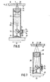
- Fig. 6 shows schematically a first embodiment of a scanning unit employing a plano-aspherical lens as the objective.
- This read unit comprises a tubular housing 30 which accommodates a diode laser 31, a beam-splitting prism 32, a collimator lens 33, and an objective in the form of a plano-aspherical lens 34.
- the reference numeral 16 indicates a small part of a radial cross-section of a round disc-shaped record carrier.
- the information structure which in the present case is radiation-reflecting, is situated on the upper side of the record carrier and comprises a multitude of information areas, not shown, arranged along information tracks 36.
- the information structure is scanned by a read beam b produced by the diode laser 31.
- the collimator forms the diverging beam into a parallel beam of such a cross-section that the pupil of the objective 34 is filled correctly.
- This objective then forms a diffraction-limited radiation spot V on the information structure.
- the read beam is reflected by the information structure and, as the record carrier moves relative to the read beam, the beam is time-modulated in conformity with the information recorded on the record carrier.
- the modulated beam is separated from the beam emitted by the diode laser and is directed towards a radiation-sensitive detection system 39. This system supplies an electric signal which is modulated in conformity with the information contained in the record carrier.
- a roof-edge prism 38 is arranged on the exit surface of the prism 32 and the detection system 39 comprises, for example, four detectors.
- the roof-edge prism splits the reflected beam into two sub-beams b 1 and b 2 which form two radiation spots V 1 and V 2 in the plane of the detection system. Each of these radiation spots is associated with two detectors.
- the tube 30 may be arranged on a slide 40, shown schematically, which slide is movable in a radial direction as indicated by the arrow 41, so that all the information tracks 36 can be scanned sequentially. Except for the outer surface 35 of the objective 34 all the elements are arranged so that the user has no access to them.
- the outer surface of the lens 34 is made of glass and is therefore highly scratch-resistant, so that it may be cleaned by the user without the risk of damage.
- plano-aspherical objective may be arranged outside the housing 30. This may be the case if the objective must be movable through small distances of the order of some tens of pm in a radial direction in order to eliminate tracking errors.
- the field of the lens in accordance with the invention is sufficiently large for this purpose.
- Another possibility is to arrange the plano-aspherical objective so as to be radially movable inside the tube 30. In the embodiment shown in Fig. 6 this fine control of the radiation spot V in a radial direction is achieved by a radial displacement of the tube 30.
- Fig. 7 shows an example of an optical scanning unit using a mono-aspherical lens with a spherical outer surface for focusing a diverging beam b' to form a diffraction-limited radiation spot on the information structure.
- This scanning unit functions in a way similar to that shown in Fig. 6.
- the advantage of the scanning unit shown in Fig. 7 is that one lens may be dispensed with, which is very important for the scanning unit which is intended as a mass product.
Landscapes
- Physics & Mathematics (AREA)
- Optics & Photonics (AREA)
- General Physics & Mathematics (AREA)
- Lenses (AREA)
- Glass Compositions (AREA)
- Macromonomer-Based Addition Polymer (AREA)
- Prostheses (AREA)
- Eyeglasses (AREA)
Claims (7)


Priority Applications (1)
| Application Number | Priority Date | Filing Date | Title |
|---|---|---|---|
| AT84201782T ATE42151T1 (de) | 1983-12-07 | 1984-12-03 | Einfache linse mit einer asphaerischen flaeche. |
Applications Claiming Priority (2)
| Application Number | Priority Date | Filing Date | Title |
|---|---|---|---|
| NL8304213A NL8304213A (nl) | 1983-12-07 | 1983-12-07 | Enkelvoudige lens met een asferisch oppervlak. |
| NL8304213 | 1983-12-07 |
Publications (2)
| Publication Number | Publication Date |
|---|---|
| EP0146178A1 EP0146178A1 (de) | 1985-06-26 |
| EP0146178B1 true EP0146178B1 (de) | 1989-04-12 |
Family
ID=19842847
Family Applications (1)
| Application Number | Title | Priority Date | Filing Date |
|---|---|---|---|
| EP84201782A Expired EP0146178B1 (de) | 1983-12-07 | 1984-12-03 | Einfache Linse mit einer asphärischen Fläche |
Country Status (12)
| Country | Link |
|---|---|
| US (1) | US4668056A (de) |
| EP (1) | EP0146178B1 (de) |
| JP (1) | JPH0614135B2 (de) |
| AT (1) | ATE42151T1 (de) |
| AU (1) | AU573659B2 (de) |
| CA (1) | CA1255527A (de) |
| DD (1) | DD229507A5 (de) |
| DE (1) | DE3477695D1 (de) |
| DK (1) | DK160109B (de) |
| ES (1) | ES8608179A1 (de) |
| NL (1) | NL8304213A (de) |
| SG (1) | SG86490G (de) |
Families Citing this family (17)
| Publication number | Priority date | Publication date | Assignee | Title |
|---|---|---|---|---|
| JPS61144616A (ja) * | 1984-12-18 | 1986-07-02 | Olympus Optical Co Ltd | 明るい広角レンズ |
| NL8502225A (nl) * | 1985-06-10 | 1987-01-02 | Philips Nv | Replika lens en methode voor de vervaardiging ervan. |
| US4768867A (en) * | 1985-09-02 | 1988-09-06 | Canon Kabushiki Kaisha | Aspherical single lens |
| JPS6310119A (ja) * | 1986-07-02 | 1988-01-16 | Matsushita Electric Ind Co Ltd | 大口径単レンズ |
| NL8603010A (nl) * | 1986-11-27 | 1988-06-16 | Philips Nv | Optische aftastinrichting. |
| JPH03502249A (ja) * | 1988-01-13 | 1991-05-23 | イーストマン・コダック・カンパニー | 薄いレンズの製造方法 |
| NL8901245A (nl) * | 1989-05-19 | 1990-12-17 | Philips Nv | Retrofokus objektieflens en optische aftastinrichting voorzien van een dergelijke lens. |
| US5153778A (en) * | 1991-06-19 | 1992-10-06 | At&T Bell Laboratories | Powerless field-corrective lens |
| JP3267089B2 (ja) * | 1994-02-22 | 2002-03-18 | キヤノン株式会社 | 走査レンズ系及びそれを用いた光走査装置 |
| JPH09500459A (ja) * | 1994-05-02 | 1997-01-14 | フィリップス エレクトロニクス ネムローゼ フェンノートシャップ | 反射防止回折格子を有する光透過性光学素子 |
| JPH08313805A (ja) * | 1995-05-18 | 1996-11-29 | Sony Corp | レンズ装置及び紫外線集光装置 |
| US5966362A (en) * | 1995-11-02 | 1999-10-12 | Konica Corporation | Optical system for recording and reproducing for use in optical information recording medium |
| KR100230253B1 (ko) * | 1996-02-14 | 1999-11-15 | 윤종용 | 대물렌즈 장치 및 이의 제작방법 및 이를 적용한 광픽업장치 |
| EP0932845B1 (de) * | 1997-08-19 | 2008-01-02 | Koninklijke Philips Electronics N.V. | Ein aberrationen begrenzendes optisches system innerhalb des maximalen abzubildenden volumens |
| JP2006505090A (ja) * | 2002-11-01 | 2006-02-09 | コーニンクレッカ フィリップス エレクトロニクス エヌ ヴィ | 光走査デバイス |
| CN101620317B (zh) * | 2008-06-30 | 2011-06-22 | 富士迈半导体精密工业(上海)有限公司 | 一种具有长焦深的激光装置 |
| JP5574226B2 (ja) * | 2010-03-23 | 2014-08-20 | 株式会社ニコン | 干渉対物レンズ及びこれを有する顕微鏡装置 |
Family Cites Families (13)
| Publication number | Priority date | Publication date | Assignee | Title |
|---|---|---|---|---|
| US2388118A (en) * | 1942-05-08 | 1945-10-30 | Vickers Electrical Co Ltd | Lens |
| US2530397A (en) * | 1948-02-18 | 1950-11-21 | Ancillary Henry L Beigel | Anastigmatic lens |
| DE1278131C2 (de) * | 1965-11-18 | 1974-03-21 | Taisuke Tsugami | Asphaerische Linse |
| US3508811A (en) * | 1966-11-09 | 1970-04-28 | Taisuke Tsugami | Aspheric lens having log cos surfaces |
| GB1362380A (en) * | 1971-11-25 | 1974-08-07 | Mullard Ltd | Manufacture of optical elements |
| JPS533926B2 (de) * | 1973-08-31 | 1978-02-13 | ||
| DE2445333A1 (de) * | 1973-10-01 | 1975-04-10 | Philips Nv | Optoelektronisches system zur bestimmung einer abweichung zwischen der istlage und der sollage einer ebene in einem optischen abbildungssystem |
| FR2271585B1 (de) * | 1974-05-14 | 1976-10-15 | Philips Nv | |
| JPS55130527A (en) * | 1979-03-30 | 1980-10-09 | Minolta Camera Co Ltd | Real image system finder optical system |
| JPS5776512A (en) * | 1980-10-31 | 1982-05-13 | Konishiroku Photo Ind Co Ltd | Large-aperture aspheric single lens |
| JPS57201210A (en) * | 1981-06-04 | 1982-12-09 | Sony Corp | Condenser lens |
| NL8103323A (nl) * | 1981-07-13 | 1983-02-01 | Philips Nv | Enkelvoudige lens met een sferisch en een asferisch brekend oppervlak. |
| JPS5868711A (ja) * | 1981-10-20 | 1983-04-23 | Matsushita Electric Ind Co Ltd | 対物レンズ |
-
1983
- 1983-12-07 NL NL8304213A patent/NL8304213A/nl not_active Application Discontinuation
-
1984
- 1984-03-14 US US06/589,909 patent/US4668056A/en not_active Expired - Lifetime
- 1984-09-29 JP JP59203021A patent/JPH0614135B2/ja not_active Expired - Lifetime
- 1984-12-03 EP EP84201782A patent/EP0146178B1/de not_active Expired
- 1984-12-03 DE DE8484201782T patent/DE3477695D1/de not_active Expired
- 1984-12-03 AT AT84201782T patent/ATE42151T1/de not_active IP Right Cessation
- 1984-12-04 DK DK575884A patent/DK160109B/da not_active Application Discontinuation
- 1984-12-04 DD DD84270266A patent/DD229507A5/de not_active IP Right Cessation
- 1984-12-04 ES ES538239A patent/ES8608179A1/es not_active Expired
- 1984-12-05 CA CA000469398A patent/CA1255527A/en not_active Expired
- 1984-12-06 AU AU36352/84A patent/AU573659B2/en not_active Ceased
-
1990
- 1990-10-24 SG SG864/90A patent/SG86490G/en unknown
Also Published As
| Publication number | Publication date |
|---|---|
| ATE42151T1 (de) | 1989-04-15 |
| ES8608179A1 (es) | 1986-06-01 |
| NL8304213A (nl) | 1985-07-01 |
| DE3477695D1 (en) | 1989-05-18 |
| US4668056A (en) | 1987-05-26 |
| AU3635284A (en) | 1985-06-13 |
| DK575884A (da) | 1985-06-08 |
| JPS60126616A (ja) | 1985-07-06 |
| SG86490G (en) | 1991-01-04 |
| DD229507A5 (de) | 1985-11-06 |
| CA1255527A (en) | 1989-06-13 |
| ES538239A0 (es) | 1986-06-01 |
| DK575884D0 (da) | 1984-12-04 |
| JPH0614135B2 (ja) | 1994-02-23 |
| DK160109B (da) | 1991-01-28 |
| AU573659B2 (en) | 1988-06-16 |
| EP0146178A1 (de) | 1985-06-26 |
Similar Documents
| Publication | Publication Date | Title |
|---|---|---|
| EP0146178B1 (de) | Einfache Linse mit einer asphärischen Fläche | |
| KR100388515B1 (ko) | 광학픽업장치 | |
| EP0146177B1 (de) | Einfache Sammellinse mit einer asphärischen Fläche | |
| JP3666632B2 (ja) | 収差補正装置及びこれを用いた光ピックアップ装置 | |
| US6480344B1 (en) | Objective lens for optical pick-up | |
| EP0721124B1 (de) | Objektiv und optischer Kopf mit einem derartigen Objektiv | |
| EP0800170B1 (de) | Optische Anordnung zum Beschreiben und/oder Lesen eines optischen Aufzeichnungsmediums | |
| JP3704833B2 (ja) | 対物レンズ及び記録再生装置 | |
| US5835473A (en) | Optical pick-up, optical data recording apparatus and objective lens for optical data recording material | |
| JPH0816738B2 (ja) | 光学式ヘッド装置 | |
| US6781764B1 (en) | Objective lens for optical pick-up | |
| JP3911104B2 (ja) | 光情報記録再生装置の光学系 | |
| JP3425845B2 (ja) | 光情報記録媒体の記録再生用光学系および対物レンズ | |
| US6775064B2 (en) | Objective lens for optical pick-up | |
| US20020122377A1 (en) | Optical head for scanning a record carrier | |
| JP4364328B2 (ja) | 高密度光記録媒体用対物レンズ | |
| US20040150892A1 (en) | Optical system of optical pick-up | |
| US7920455B2 (en) | Complex optical element and optical pickup | |
| US5889749A (en) | Optical pickup apparatus | |
| JPH0140325B2 (de) | ||
| US20040213132A1 (en) | Optical system of optical pick-up | |
| US20060067204A1 (en) | Objective lens and scanning device using such an objective lens | |
| JPS62194212A (ja) | 光学式情報読取装置の対物レンズ | |
| JP4375107B2 (ja) | 光ピックアップ装置 | |
| US7787349B2 (en) | Optical pickup lens and optical pickup apparatus |
Legal Events
| Date | Code | Title | Description |
|---|---|---|---|
| PUAI | Public reference made under article 153(3) epc to a published international application that has entered the european phase |
Free format text: ORIGINAL CODE: 0009012 |
|
| AK | Designated contracting states |
Designated state(s): AT BE CH DE FR GB IT LI SE |
|
| 17P | Request for examination filed |
Effective date: 19851218 |
|
| 17Q | First examination report despatched |
Effective date: 19870127 |
|
| D17Q | First examination report despatched (deleted) | ||
| GRAA | (expected) grant |
Free format text: ORIGINAL CODE: 0009210 |
|
| AK | Designated contracting states |
Kind code of ref document: B1 Designated state(s): AT BE CH DE FR GB IT LI SE |
|
| REF | Corresponds to: |
Ref document number: 42151 Country of ref document: AT Date of ref document: 19890415 Kind code of ref document: T |
|
| REF | Corresponds to: |
Ref document number: 3477695 Country of ref document: DE Date of ref document: 19890518 |
|
| ITF | It: translation for a ep patent filed | ||
| ET | Fr: translation filed | ||
| PGFP | Annual fee paid to national office [announced via postgrant information from national office to epo] |
Ref country code: BE Payment date: 19891220 Year of fee payment: 6 |
|
| PGFP | Annual fee paid to national office [announced via postgrant information from national office to epo] |
Ref country code: SE Payment date: 19891228 Year of fee payment: 6 Ref country code: AT Payment date: 19891228 Year of fee payment: 6 |
|
| PLBE | No opposition filed within time limit |
Free format text: ORIGINAL CODE: 0009261 |
|
| STAA | Information on the status of an ep patent application or granted ep patent |
Free format text: STATUS: NO OPPOSITION FILED WITHIN TIME LIMIT |
|
| PGFP | Annual fee paid to national office [announced via postgrant information from national office to epo] |
Ref country code: CH Payment date: 19900321 Year of fee payment: 6 |
|
| 26N | No opposition filed | ||
| PG25 | Lapsed in a contracting state [announced via postgrant information from national office to epo] |
Ref country code: AT Effective date: 19901203 |
|
| PG25 | Lapsed in a contracting state [announced via postgrant information from national office to epo] |
Ref country code: SE Effective date: 19901204 |
|
| PG25 | Lapsed in a contracting state [announced via postgrant information from national office to epo] |
Ref country code: LI Effective date: 19901231 Ref country code: CH Effective date: 19901231 Ref country code: BE Effective date: 19901231 |
|
| BERE | Be: lapsed |
Owner name: PHILIPS' GLOEILAMPENFABRIEKEN N.V. Effective date: 19901231 |
|
| REG | Reference to a national code |
Ref country code: CH Ref legal event code: PL |
|
| ITTA | It: last paid annual fee | ||
| EUG | Se: european patent has lapsed |
Ref document number: 84201782.4 Effective date: 19910910 |
|
| ITPR | It: changes in ownership of a european patent |
Owner name: CAMBIO RAGIONE SOCIALE;PHILIPS ELECTRONICS N.V. |
|
| REG | Reference to a national code |
Ref country code: FR Ref legal event code: CD |
|
| REG | Reference to a national code |
Ref country code: FR Ref legal event code: CD |
|
| PGFP | Annual fee paid to national office [announced via postgrant information from national office to epo] |
Ref country code: GB Payment date: 20001220 Year of fee payment: 17 |
|
| PGFP | Annual fee paid to national office [announced via postgrant information from national office to epo] |
Ref country code: FR Payment date: 20001226 Year of fee payment: 17 |
|
| PGFP | Annual fee paid to national office [announced via postgrant information from national office to epo] |
Ref country code: DE Payment date: 20010214 Year of fee payment: 17 |
|
| PG25 | Lapsed in a contracting state [announced via postgrant information from national office to epo] |
Ref country code: GB Free format text: LAPSE BECAUSE OF NON-PAYMENT OF DUE FEES Effective date: 20011203 |
|
| REG | Reference to a national code |
Ref country code: GB Ref legal event code: IF02 |
|
| PG25 | Lapsed in a contracting state [announced via postgrant information from national office to epo] |
Ref country code: DE Free format text: LAPSE BECAUSE OF NON-PAYMENT OF DUE FEES Effective date: 20020702 |
|
| GBPC | Gb: european patent ceased through non-payment of renewal fee |
Effective date: 20011203 |
|
| PG25 | Lapsed in a contracting state [announced via postgrant information from national office to epo] |
Ref country code: FR Free format text: LAPSE BECAUSE OF NON-PAYMENT OF DUE FEES Effective date: 20020830 |
|
| REG | Reference to a national code |
Ref country code: FR Ref legal event code: ST |