EP0144545B1 - Diffusionsverfahren zum Herstellen eines Thyristors - Google Patents
Diffusionsverfahren zum Herstellen eines Thyristors Download PDFInfo
- Publication number
- EP0144545B1 EP0144545B1 EP84110190A EP84110190A EP0144545B1 EP 0144545 B1 EP0144545 B1 EP 0144545B1 EP 84110190 A EP84110190 A EP 84110190A EP 84110190 A EP84110190 A EP 84110190A EP 0144545 B1 EP0144545 B1 EP 0144545B1
- Authority
- EP
- European Patent Office
- Prior art keywords
- emitter
- type impurity
- thyristor
- diffusing
- wafer
- Prior art date
- Legal status (The legal status is an assumption and is not a legal conclusion. Google has not performed a legal analysis and makes no representation as to the accuracy of the status listed.)
- Expired
Links
Images


Classifications
-
- H—ELECTRICITY
- H10—SEMICONDUCTOR DEVICES; ELECTRIC SOLID-STATE DEVICES NOT OTHERWISE PROVIDED FOR
- H10D—INORGANIC ELECTRIC SEMICONDUCTOR DEVICES
- H10D18/00—Thyristors
-
- H—ELECTRICITY
- H10—SEMICONDUCTOR DEVICES; ELECTRIC SOLID-STATE DEVICES NOT OTHERWISE PROVIDED FOR
- H10D—INORGANIC ELECTRIC SEMICONDUCTOR DEVICES
- H10D18/00—Thyristors
- H10D18/60—Gate-turn-off devices
-
- H—ELECTRICITY
- H10—SEMICONDUCTOR DEVICES; ELECTRIC SOLID-STATE DEVICES NOT OTHERWISE PROVIDED FOR
- H10D—INORGANIC ELECTRIC SEMICONDUCTOR DEVICES
- H10D62/00—Semiconductor bodies, or regions thereof, of devices having potential barriers
- H10D62/80—Semiconductor bodies, or regions thereof, of devices having potential barriers characterised by the materials
- H10D62/83—Semiconductor bodies, or regions thereof, of devices having potential barriers characterised by the materials being Group IV materials, e.g. B-doped Si or undoped Ge
- H10D62/834—Semiconductor bodies, or regions thereof, of devices having potential barriers characterised by the materials being Group IV materials, e.g. B-doped Si or undoped Ge further characterised by the dopants
-
- H—ELECTRICITY
- H10—SEMICONDUCTOR DEVICES; ELECTRIC SOLID-STATE DEVICES NOT OTHERWISE PROVIDED FOR
- H10P—GENERIC PROCESSES OR APPARATUS FOR THE MANUFACTURE OR TREATMENT OF DEVICES COVERED BY CLASS H10
- H10P32/00—Diffusion of dopants within, into or out of wafers, substrates or parts of devices
- H10P32/10—Diffusion of dopants within, into or out of semiconductor bodies or layers
- H10P32/14—Diffusion of dopants within, into or out of semiconductor bodies or layers within a single semiconductor body or layer in a solid phase; between different semiconductor bodies or layers, both in a solid phase
- H10P32/1404—Diffusion of dopants within, into or out of semiconductor bodies or layers within a single semiconductor body or layer in a solid phase; between different semiconductor bodies or layers, both in a solid phase using predeposition followed by drive-in of impurities into the semiconductor surface, e.g. predeposition from a gaseous phase
-
- H—ELECTRICITY
- H10—SEMICONDUCTOR DEVICES; ELECTRIC SOLID-STATE DEVICES NOT OTHERWISE PROVIDED FOR
- H10P—GENERIC PROCESSES OR APPARATUS FOR THE MANUFACTURE OR TREATMENT OF DEVICES COVERED BY CLASS H10
- H10P32/00—Diffusion of dopants within, into or out of wafers, substrates or parts of devices
- H10P32/10—Diffusion of dopants within, into or out of semiconductor bodies or layers
- H10P32/17—Diffusion of dopants within, into or out of semiconductor bodies or layers characterised by the semiconductor material
- H10P32/171—Diffusion of dopants within, into or out of semiconductor bodies or layers characterised by the semiconductor material being group IV material
-
- Y—GENERAL TAGGING OF NEW TECHNOLOGICAL DEVELOPMENTS; GENERAL TAGGING OF CROSS-SECTIONAL TECHNOLOGIES SPANNING OVER SEVERAL SECTIONS OF THE IPC; TECHNICAL SUBJECTS COVERED BY FORMER USPC CROSS-REFERENCE ART COLLECTIONS [XRACs] AND DIGESTS
- Y10—TECHNICAL SUBJECTS COVERED BY FORMER USPC
- Y10S—TECHNICAL SUBJECTS COVERED BY FORMER USPC CROSS-REFERENCE ART COLLECTIONS [XRACs] AND DIGESTS
- Y10S438/00—Semiconductor device manufacturing: process
- Y10S438/904—Charge carrier lifetime control
Definitions
- the present invention relates to a method for fabricating a thyristor.
- a high-voltage direct-current-transmission system must be able to handle a voltage of several kilovolts to several hundred kilovolts. Such a system frequently comprises one hundred or more series-connected thyristors.
- a conventional single thyristor which is generally used has an off-state voltage (blocking voltage) of only about several kilovolts.
- an off-state voltage of a thyristor must be increased.
- a conventional thyristor is fabricated in the following manner. P-type impurities are diffused in two surfaces of an n-type Si substrate to obtain a pnp wafer having a p-emitter and p-and n-bases. A portion of a surface of the p-base is etched to control the thickness thereof. Thereafter, oxide films are formed on two surfaces of the pnp wafer. A portion of one oxide film is removed by a known photoetching process. n-type impurities are selectively diffused in the p-base to form an n +- emitter. In this process, phosphorus (P) is deposited to several micrometers, and is then driven in at a high temperature.
- P phosphorus
- the n+-emitter has a depth of about 20 ⁇ m.
- p-type impurities are diffused in two surfaces of the obtained pnpn wafer to have a high surface impurity concentration but a lower concentration than that of the n+-emitter, thereby forming a p + -layer.
- a heavy metal such as gold (Au) is diffused in the pnpn wafer obtained as described above.
- predetermined electrodes are formed on the resultant structure.
- a thickness and a resistivity of the n-base must be increased.
- a thyristor used in a direct current transmission system described above must have an on-state voltage (VF) of about 3 V or less at a current density (J) of about 100 to 150 A ⁇ cm -2 , a turn-off time (tq) of 500 ⁇ sec or less, and variations in a reverse recovery charge (Qrr) of ⁇ 20% or less.
- VF on-state voltage
- J current density
- tq turn-off time
- Qrr reverse recovery charge
- a maximum off-state voltage is 4 kV which satisfies the above conditions.
- a thyristor having an off-state voltage of more than 4 kV cannot be practically obtained.
- gettering is performed on a pnp wafer. Thereafter, phosphorus is diffused at a low temperature to form an n+-emitter.
- gettering is performed on a pnpn wafer immediately before a gold diffusion process.
- a thyristor which satisfies the above conditions and has an off-state voltage of more than 6 kV cannot be practically obtained.
- the n+-emitter is formed at a low temperature after the gettering process, thereby undesirably prolonging a heating process.
- a plurality of defects are introduced. These defects getter a heavy metal. Therefore, a carrier lifetime of p- and n-bases in the vicinity of the n + -emitter is undesirably prolonged, thereby excessively prolonging a turn-off time of a thyristor.
- the gettering is performed after forming the n +- emitter. A plurality of defects are introduced in the same manner as the former method. In this method, a carrier lifetime is finally controlled by gold diffusion.
- a thyristor which has an off-state voltage of more than 6 kV and a sufficiently small on-state voltage (VF) and turn-off time (tq) cannot be obtained.
- n+-emitter when the n+-emitter is formed, impurities are diffused to have a high concentration. As a result, a plurality of defects are formed, thereby degrading the characteristics of a thyristor.
- the present invention provides a method for fabricating a thyristor comprising the following sequence of steps:
- p-type impurities are diffused in two surfaces of an n-type Si substrate to form a pnp wafer having a p-emitter, and n- and p-bases. Thereafter, then n-type impurities are diffused in the surface of the p-base to form an n+-emitter, the amounts of doped impurities are controlled not to exceed the amounts of the impurities which are electrically activated, thereby controlling the formation of defects then the n+-emitter is formed. n-type impurities are diffused in two surfaces of the thus obtained pnpn wafer to have high concentration and to small depths, and thereafter gettering is performed.
- a diffusion source is maintained at a low temperature, and an amount of a carrier gas is controlled.
- the pnpn wafer is heated in an inert gas at a temperature of 600 to 1,000°C for up to 10 hours, thereby further decreasing variations in characteristics of the obtained thyristor.
- the defect density is controlled.
- a high voltage thyristor having a low on-state voltage, a short turn-off time, and small variations in reverse recovery charge can be obtained.
- This thyristor can be effectively employed in a high voltage direct current transmission system.
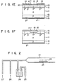
- p-type impurities are diffused in two surfaces of an n-type Si substrate to form a pnp wafer consisting of n- and p-bases 11 and 12 and a p-emitter 13.
- the resistivity of a starting substrate, i.e., the n-base 11 is set at about 200 ⁇ cm, and in order to obtain a 6-kV thyristor, it is set at about 300 ⁇ cm.
- a thickness of the n-base 11 is set at about 800 pm, and in the 6-kV thyristor, it is set at about 1,100 ⁇ m.
- the p-base 12 and the p-emitter 13 have a thickness of about 80 to 150 ⁇ m and a surface impurity concentration of about 10 19 cm- 3 .
- a portion of the p-base 12 is etched to have a thickness of 60 to 70 ⁇ m, as shown in Figure 1B.
- Oxide (Si0 2 ) films 14 are simultaneously formed on two surfaces of the pnp wafer by thermal oxidation.
- a portion of one of the oxide films 14 at the side of the p-base 12 is removed by a known photoetching process. Phosphorus is diffused using the remaining oxide film 14 as a mask so as to form an n+-emitter 15.
- the depth of the n+-emitter 15 is 5 to 20 ⁇ m.
- the main feature of the present invention lies in the process of depositing the phosphorus, and it will be described in detail hereafter.
- This phosphorus deposition process is performed using, for. example, a reactor shown in Figure 2.
- reference numeral 21 denotes a reaction tube.
- Each pnp wafer 22 is supported on a boat 23 and is placed in the reaction tube 21.
- Reference numeral 24 denotes POCI 3 as a diffusion source; 25 denotes an N 2 gas for carrying the diffusion source 24; 26 denotes a O2 gas; and 27 denotes a main N 2 gas for carrying all the diffusion source 24, the N 2 gas 25 and the O2 gas 26.
- the amount of the POCI 3 supplied as the diffusion source 24 is controlled by using this reactor, and a given amount of phosphorus which can be electrically activated is deposited. More specifically, the temperature of the diffusion source 24 is maintained at less than 5°C. Furthermore, respective relative flow rates of the N 2 and O2 gases 25 and 26 are set at 1/20 or less of that of the main N 2 gas 27. After performing the phosphorus deposition described above under these conditions, the phosphorus is driven in at a temperature of 1,200°C for 1 hour. As a result, the n+-emitter 15 has a surface impurity concentration of about 10 2 ° cm- 3 and all the doped phosphorus is electrically activated. Almost no defects occur in the n+-emitter 15.
- p + -layers 16 and 17 are formed on two surfaces of the pnpn wafer by diffusing, e.g. gallium (Ga) so as to provide a good ohmic contact. Since the gallium passes through the oxide film 14, the oxide films 14 do not have to be removed.
- Ga gallium
- n ++ -layers 18 and 19 are formed by diffusing n-type impurities such as phosphorus so as to respectively have a high impurity concentration and a shallow depth.
- This gettering process is performed using the reactor of Figure 2 while maintaining the diffusion source 24 at or above room temperature. In this manner, the n ++- layer 18 having a plurality of defects is formed to a depth of several micrometers from the surface of the n+-emitter 15.
- the gettering process can be performed on the entire two surfaces of the pnpn wafer after removing all the oxide films 14. In this case, an n ++ -layer formed on the p-base 12 must be later removed.
- the n ++ -layer 19 at the anode side is removed. Then, a heavy metal such as gold (Au) is diffused in this resultant pnpn wafer, thereby controlling a carrier lifetime of the n- and p-bases 11 and 12. In this case, the n ++- layer 19 can be removed after performing this carrier lifetime control process.
- Au gold
- predetermined electrodes are formed on the resultant wafer and then a thyristor is formed.
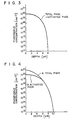
- Figure 3 shows a phosphorus concentration distribution of the n+-emitter 15 formed according to this embodiment.
- the profile which represents the total amount of the phosphorus by neutron activated analysis completely coincides with that of the total amount of the electrically activated phosphorus.
- Figure 4 shows the phosphorus concentration distribution of an n+-emitter formed according to a conventional process described in U.S.P. No. 4,370,810, for reference.
- the n +- emitter diffusion process is performed using the reactor of Figure 2 in the following manner.
- the diffusion source is maintained at room temperature, and respective relative flow rates of the N 2 and O2 gases 25 and 26 are set at 1/4 of that of the main N 2 gas 27.
- the phosphorus is deposited and annealed at a temperature of 1,100°C for 1 hour.
- a difference between the total amount A of the phosphorus and the total amount B of the activated phosphorus can be found. In this manner, when the phosphorus is excessively doped, the n+-emitter has a plurality of defects.
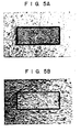
- Figures 5A and 5B are microphotographs (at a magnification of 100) respectively showing a defect distribution of the surface of the n+-emitter of the prior art having the profile shown in Figure 4 and that of the surface of the n+-emitter of this embodiment having the profile shown in Figure 3.
- the respective n+-emitters were diffused in only the rectangular portions of the respective p-bases, and then the respective surfaces thereof were etched by using a known "Sirti" etching solution for detecting defects.
- the microphotographs described above were taken of the respective surfaces of the n +- emitters.
- Figure 6 show changes in a carrier lifetime according to this embodiment.
- the carrier lifetime is not increased by the n *- emitter diffusion process, but is increased after the gettering process. Thereafter, a desired carrier lifetime can be obtained by the gold diffusion process.
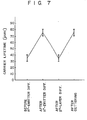
- Figure 7 shows changes in a carrier lifetime according to the conventional process wherein the n+-emitter having the profile of Figure 4 is formed.
- the carrier lifetime is greatly increased by the n + -emitter diffusion process.
- the increased carrier lifetime is decreased once by the player diffusion process and is increased again by the gettering process.
- the defects introduced by the n+-emitter diffusion process still remain unremoved. These defects prevent the control of the carrier lifetime by the gold diffusion process. Therefore, it is difficult to obtain the desired thyristor characteristics.
- Figure 8 shows a relationship between off-state voltages and on-state voltages of the thyristors respectively formed according to this embodiment and the prior art having the different n +- emitter diffusion process from that of the embodiment.
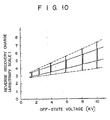
- Figures 9 and 10 show relationships between off-state voltages and turn-off times and between off-state voltages and reverse recovery charges, respectively, of these thyristors.
- solid curves correspond to the embodiment of the present invention and dotted curves correspond to the prior art.
- the thyristor according to this embodiment has a small on-state voltage, a short turn-off time and small variations in a reverse recovery charge in comparison with those of the prior art. In particular, this effect is particularly notable in a thyristor having a large off-state voltage.
- the processes shown in the present invention are merely one example, and the main feature of the present invention lies in a combination of a particular forming method of an n-emitter and gettering.
- the pnpn wafer may be annealed in an inert gas at a temperature of 1,000°C for up to 10 hours, thereby further reducing variations in the characteristics of the thyristor.
- the conditions for the n + -emitter diffusion process can be set so as to leave no inactivated n-type impurities.
- the phosphorus deposition conditions are set as follows so as to obtain the results below.
- the temperature of phosphorus diffusion is set at 900 to 1,000°C
- the surface impurity concentration becomes 5 ⁇ 10 19 to 7 ⁇ 10 19 cm- 3 .
- the temperature of phosphorus diffusion is set at 1,000 to 1,200°C
- the surface impurity concentration becomes 7 ⁇ 10 19 to 10 20 cm- 3 . Therefore, an n+-emitter having almost no defects can be obtained.
- the present invention can be employed not only in a normal thyristor, but also in a gate turn-off thyristor (GTO), a thyristor in which a reverse conducting diode is integrally formed, a light- triggered thyristor, and the like.
- GTO gate turn-off thyristor
- a thyristor in which a reverse conducting diode is integrally formed a light- triggered thyristor, and the like.
Landscapes
- Thyristors (AREA)
Claims (3)
dadurch gekennzeichnet, daß der Diffusionsprozeß des Schrittes (b) zum Bilden des n+- Emitters (15) durch eine selektive Ablagerung eines n-Typ-Fremdstoffes und eine anschließende Eintriebsstufe bei einer vorbestimmten Temperatur durchgeführt wird, wobei die Menge des aufgetragenen n-Typ-Fremdstoffes und die Eintriebstemperatur derart gesteuert sind, daß der gesamte diffundierte Fremdstoff, der den n+- Emitter bildet, elektrisch aktiviert wird.
Applications Claiming Priority (2)
| Application Number | Priority Date | Filing Date | Title |
|---|---|---|---|
| JP224075/83 | 1983-11-30 | ||
| JP58224075A JPS60117665A (ja) | 1983-11-30 | 1983-11-30 | サイリスタの製造方法 |
Publications (3)
| Publication Number | Publication Date |
|---|---|
| EP0144545A2 EP0144545A2 (de) | 1985-06-19 |
| EP0144545A3 EP0144545A3 (en) | 1987-03-25 |
| EP0144545B1 true EP0144545B1 (de) | 1990-03-21 |
Family
ID=16808164
Family Applications (1)
| Application Number | Title | Priority Date | Filing Date |
|---|---|---|---|
| EP84110190A Expired EP0144545B1 (de) | 1983-11-30 | 1984-08-27 | Diffusionsverfahren zum Herstellen eines Thyristors |
Country Status (4)
| Country | Link |
|---|---|
| US (1) | US4613381A (de) |
| EP (1) | EP0144545B1 (de) |
| JP (1) | JPS60117665A (de) |
| DE (1) | DE3481743D1 (de) |
Families Citing this family (5)
| Publication number | Priority date | Publication date | Assignee | Title |
|---|---|---|---|---|
| JPS6115366A (ja) * | 1984-06-30 | 1986-01-23 | Mitsuo Kusano | ゲ−トタ−ンオフサイリスタ及びその製造方法 |
| JPH0770476B2 (ja) * | 1985-02-08 | 1995-07-31 | 株式会社東芝 | 半導体装置の製造方法 |
| DE3941932A1 (de) * | 1989-12-19 | 1991-06-20 | Eupec Gmbh & Co Kg | Verfahren zum herstellen von anodenseitigen kurzschluessen in thyristoren |
| GB2524699C (en) * | 2013-02-07 | 2018-11-14 | Wood John | A bipolar junction transistor structure |
| CN108292669B (zh) * | 2015-09-11 | 2019-08-02 | Abb瑞士股份有限公司 | 关断型功率半导体器件及其制造方法 |
Family Cites Families (5)
| Publication number | Priority date | Publication date | Assignee | Title |
|---|---|---|---|---|
| US3821038A (en) * | 1972-05-22 | 1974-06-28 | Ibm | Method for fabricating semiconductor structures with minimum crystallographic defects |
| JPS54102864A (en) * | 1978-01-31 | 1979-08-13 | Toshiba Corp | Diffusion method for impurity |
| JPS5543863A (en) * | 1978-09-25 | 1980-03-27 | Hitachi Ltd | Manufacture of semiconductor element |
| DE3037316C2 (de) * | 1979-10-03 | 1982-12-23 | Tokyo Shibaura Denki K.K., Kawasaki, Kanagawa | Verfahren zur Herstellung von Leistungsthyristoren |
| JPS5766628A (en) * | 1980-10-13 | 1982-04-22 | Toshiba Corp | Manufacture of semiconductor device |
-
1983
- 1983-11-30 JP JP58224075A patent/JPS60117665A/ja active Pending
-
1984
- 1984-08-27 DE DE8484110190T patent/DE3481743D1/de not_active Expired - Lifetime
- 1984-08-27 EP EP84110190A patent/EP0144545B1/de not_active Expired
- 1984-08-27 US US06/644,257 patent/US4613381A/en not_active Expired - Lifetime
Also Published As
| Publication number | Publication date |
|---|---|
| US4613381A (en) | 1986-09-23 |
| JPS60117665A (ja) | 1985-06-25 |
| DE3481743D1 (de) | 1990-04-26 |
| EP0144545A2 (de) | 1985-06-19 |
| EP0144545A3 (en) | 1987-03-25 |
Similar Documents
| Publication | Publication Date | Title |
|---|---|---|
| EP0134166B1 (de) | Plättchenherstellung mittels Implantation durch Schutzschichten | |
| US4725874A (en) | Semiconductor device having protected edges | |
| EP0345435B2 (de) | Halbleiteranordnung mit hoher Durchbruchspannung und Verfahren für ihre Herstellung | |
| EP0327316A2 (de) | Halbleitervorrichtung mit zusammengesetztem Substrat, hergestellt aus zwei Halbleitersubstraten in engem Kontakt | |
| EP0299062B1 (de) | Verfahren zur herstellung dünner einzelkristallsiliciuminseln auf einem isolator | |
| US4370180A (en) | Method for manufacturing power switching devices | |
| EP0044426B1 (de) | Verfahren zum Herstellen einer integrierten Injektions-Logikschaltung | |
| JPH05347413A (ja) | 半導体装置の製造方法 | |
| US3982269A (en) | Semiconductor devices and method, including TGZM, of making same | |
| EP0160525B1 (de) | GTO-Thyristor und Verfahren zu dessen Herstellung | |
| US4151011A (en) | Process of producing semiconductor thermally sensitive switching element by selective implantation of inert ions in thyristor structure | |
| EP2006894B1 (de) | Verfahren zur Herstellung eines Halbleiterbauelements | |
| EP0144545B1 (de) | Diffusionsverfahren zum Herstellen eines Thyristors | |
| EP0180457B1 (de) | Halbleiteranordnung mit einer integrierten Schaltung und Verfahren zu deren Herstellung | |
| EP0107437B1 (de) | Verfahren zum Herstellen eines aus einem bipolaren Transistor und einer Schottky-Diode bestehenden Halbleiterbauelementes | |
| US5223442A (en) | Method of making a semiconductor device of a high withstand voltage | |
| EP0190934B1 (de) | Verfahren zum Herstellen eines Thyristors | |
| JPH0738102A (ja) | 高耐圧半導体装置の製造方法 | |
| US6146947A (en) | Insulated gate type field effect transistor and method of manufacturing the same | |
| JP2003517204A (ja) | 炭化ケイ素半導体装置においてより高い反転層移動度を得る方法 | |
| EP0101739B1 (de) | Transistor mit Heteroübergang und Verfahren zu dessen Herstellung | |
| EP0206136B1 (de) | Verfahren zum Herstellen einer Halbleiteranordnung | |
| CA1205577A (en) | Semiconductor device | |
| EP0774167B1 (de) | Leistungshalbleiteranordnung | |
| CN116547788B (zh) | 半导体装置的制造方法以及半导体装置 |
Legal Events
| Date | Code | Title | Description |
|---|---|---|---|
| PUAI | Public reference made under article 153(3) epc to a published international application that has entered the european phase |
Free format text: ORIGINAL CODE: 0009012 |
|
| 17P | Request for examination filed |
Effective date: 19840924 |
|
| AK | Designated contracting states |
Designated state(s): CH DE LI SE |
|
| PUAL | Search report despatched |
Free format text: ORIGINAL CODE: 0009013 |
|
| AK | Designated contracting states |
Kind code of ref document: A3 Designated state(s): CH DE LI SE |
|
| 17Q | First examination report despatched |
Effective date: 19881212 |
|
| RBV | Designated contracting states (corrected) |
Designated state(s): DE |
|
| GRAA | (expected) grant |
Free format text: ORIGINAL CODE: 0009210 |
|
| AK | Designated contracting states |
Kind code of ref document: B1 Designated state(s): DE |
|
| REF | Corresponds to: |
Ref document number: 3481743 Country of ref document: DE Date of ref document: 19900426 |
|
| PLBE | No opposition filed within time limit |
Free format text: ORIGINAL CODE: 0009261 |
|
| STAA | Information on the status of an ep patent application or granted ep patent |
Free format text: STATUS: NO OPPOSITION FILED WITHIN TIME LIMIT |
|
| 26N | No opposition filed | ||
| PGFP | Annual fee paid to national office [announced via postgrant information from national office to epo] |
Ref country code: DE Payment date: 19970905 Year of fee payment: 14 |
|
| PG25 | Lapsed in a contracting state [announced via postgrant information from national office to epo] |
Ref country code: DE Free format text: LAPSE BECAUSE OF NON-PAYMENT OF DUE FEES Effective date: 19990601 |