EP0142819A2 - Zugriffsteuerungsanordnung für einen Speicher mit Hardware- und Softwarebereichen - Google Patents
Zugriffsteuerungsanordnung für einen Speicher mit Hardware- und Softwarebereichen Download PDFInfo
- Publication number
- EP0142819A2 EP0142819A2 EP84113746A EP84113746A EP0142819A2 EP 0142819 A2 EP0142819 A2 EP 0142819A2 EP 84113746 A EP84113746 A EP 84113746A EP 84113746 A EP84113746 A EP 84113746A EP 0142819 A2 EP0142819 A2 EP 0142819A2
- Authority
- EP
- European Patent Office
- Prior art keywords
- address
- storage
- access control
- registration means
- access
- Prior art date
- Legal status (The legal status is an assumption and is not a legal conclusion. Google has not performed a legal analysis and makes no representation as to the accuracy of the status listed.)
- Granted
Links
Images

Classifications
-
- G—PHYSICS
- G06—COMPUTING; CALCULATING OR COUNTING
- G06F—ELECTRIC DIGITAL DATA PROCESSING
- G06F12/00—Accessing, addressing or allocating within memory systems or architectures
- G06F12/14—Protection against unauthorised use of memory or access to memory
- G06F12/1416—Protection against unauthorised use of memory or access to memory by checking the object accessibility, e.g. type of access defined by the memory independently of subject rights
- G06F12/145—Protection against unauthorised use of memory or access to memory by checking the object accessibility, e.g. type of access defined by the memory independently of subject rights the protection being virtual, e.g. for virtual blocks or segments before a translation mechanism
Definitions
- the present invention ralates to an access control system for a storage having an area for hardware and an area for software.
- a storage for example, a main storage has not only a software area (hereinafter referred to as "SA") for storing ordinary programs but also a hardware area (hereinafter referred to as "HA”) which is inaccessible to the ordinary programs and used only by hardware.
- SA software area
- HA hardware area
- the SA includes addresses lower than a boundary address
- HA hardware information
- Ordinary programs are stored in the SA, and information used by the hardware of a data processing system (that is, hardware information) is stored in the HA.
- a Japanese patent application Laid-open No. 56-124952 discloses a system for inhibiting ordinary programs from accessing the HA.
- a boundary address for partitioning a main storage into an SA and an HA is previously set in a register, and an address at which the main storage is to be accessed, is compared with the boundary address by means of a comparator.
- the access to the main storage is allowed, even when the to-be-accessed address of the main storage is greater in address number than the boundary address.
- the access mode of the system is not in the HA access mode, when it is judged by the comparator that the to-be-accessed address of the main storage is greater in address number than the boundary address, the addressing exception occurs, and the access to the main storage is inhibited.
- Such addressing-exception detecting means is provided on both the central processing unit side and the storage controller side, for the following reasons.
- a storage controller is connected to an input/output processor as well as to a central processing unit.
- the addressing-exception detecting means in the storage controller In order to check the HA access from the input/ output processor, it is required to provided the addressing-exception detecting means in the storage controller.
- the addressing-exception detecting means in the storage controller is used for checking the HA access from the central processing unit, a time necessary for detecting the addressing exception becomes long, and thus it is impossible to carry out an interrupt action successfully. Therefore it is required to provide the addressing-exception detecting means in the central processing unit.
- the HA is devided into sub-areas and the sub-areas are separated from each other in the main storage, it is required to provide two boundary registers (for start and end addresses of sub-area) and two comparators (for start and end addresses of sub-area) for each of the sub-areas. That is, the number of boundary registers (or comparators) required is twice larger than the number of hardware sub-areas, and thus the amount of harware is greatly increased.
- An object of the present invention is to provide an improved access control system for storage.
- Another object of the present invention is to provide an access control system capable of simplifying the addressing-exception detecting means.
- a data processing system In order to carry out the translation of a logical address into a real address at high speed, a data processing system includes a translation lookaside buffer (hereinafter referred to as "TLB”) for storing pairs of logical and real addresses which are frequently used. Further, in order to store a copy of data which is contained in a main storage and is frequently used, in a buffer storage (that is, a cache) and to utilize the above copy, the data processing system includes a buffer address array (hereinafter referred to as "BAA”) for holding an address at which the above data is stored in the main storage.
- TLB translation lookaside buffer
- BAA buffer address array
- each entry of the TLB or BAA has a flag for indicating whether an address set in the entry is included in the HA or not.
- the flag is read out from the TLB or B AA, and used for controlling the access to the main storage.
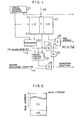
- Fig. 1 is a block diagram of an embodiment of the present invention.
- a TLB 20 has 512 entries whose addresses are assigned numbers 0 through 511, by way of example.
- Each entry of the TLB 20 includes a flag (that is, an F bit) for indicating whether a real address in the entry is included in an HA or not, in addition to the real address and a logical address.
- the F bit takes-a-value "1" or "0" according as the real address in the entry is included in the HA or SA, respectively.
- Fig. 2 shows a main storage, which is divided into an SA having lower addresses and an HA having higher addresses.
- a logical address which is given when the access to the main storage is requested is set in a logical address register 21.
- a predetermined logical operation namely, hashing
- nine bits of the logical address bits of the logical address register 21 are used to access the TLB 20, that is, to read out an entry thereof.
- a comparator 22 compares a logical address read out from the TLB 20 with upper bits of the register 21 other than the bits used for accessing the TLB 20, and outputs a logical value "1" when the upper bits of the register 21 coincide with the read-out logical address.
- the output of the comparator 22 is applied to an access control circuit 23, together with an F bit which is read out from an entry of the TLB 20 where the above real address exists.
- the access control circuit 23 is further supplied with an HA access mode bit from a signal line 13. The bit from the signal line 13 takes a value "1" when the data processing system is operated in the HA access mode, and takes a value "0" when the access mode of the system is not the HA access mode.
- Fig. 3 shows a table for explaining the operation of the access control circuit 23. That is, the meanings indicated by the combination of the inputs of the access control circuit 23 (namely, the HA access bit, the F bit, and the output of the comparator 22) and the output of the access control circuit 23 are listed in Fig. 3. Referring to Fig. 3, in the case where the output of the comparator 22 takes the level "0", the "Not in TLB” state is indicated. In this case, the output of the access control circuit 23 takes a level "0", irrespective of the values of the HA access mode bit and F bit.
- the output of the comparator 22 takes the level "1", and thus the "In TLB” state is indicated
- the output of the access control circuit 23 and the possibility of access vary depending on the values of the HA access mode bit and F bit. That is, when the F bit takes the value "0", the access to the SA is indicated, and the output of the access control circuit 23 takes the level “0” irrespective of the value of the HA access mode bit. This indicates that the "In TLB" state is utilized and the access to the main storage is allowed, as will be explained later.
- the F bit takes the value "I”
- the output of the access control circuit 23 and the possibility of access vary depending upon the value of the HA access mode bit.
- the HA access mode bit takes the value "1"
- the data processing system is operated in the HA access mode and the HA is to be accessed
- the output of the access control circuit 23 takes the level "0". That is, the "In TLB” state is utilized, and the access to the main storage is allowed.
- the HA access mode bit takes the value "0”
- the access to the HA is required in the state that the access mode of the system is not the HA access mode, and the output of the access control circuit 23 takes a level "1".
- the output of the access control circuit 23 is applied to an OR circuit 24, together with a signal which is supplied by a signal line 14 and indicates another addressing-exception generated in the data processing system.
- the OR circuit 24 delivers an output having the level "1", that is, an addressing-exception signal.
- the output of the OR circuit 24 is also applied to an AND circuit 26 through an inverter 25.
- the AND circuit 26 is closed, and therefore prevents the real address read out of the TLB 20 from being transferred to the main storage.
- the real address read out of the TLB 20 is delivered through the AND circuit 26.
- the real address thus delivered is combined with lower address bits of the logical address register 21.
- the resultant address is sent to a storage controller, and then transferred to the main storage to be used for accessing the main storage.
- an address translation step is started, and a new pair of logical and real addresses is registered in the TLB 20.
- the above address translation step is well known, and therefore further explanation thereof will be omitted.
- the new address pair is registered in the TLB 20
- an F bit which is supplied from the storage controller through a signal line 28 is registered in an entry of the TLB where the new address pair is set. That is, the storage controller includes addressing-exception detecting means shown in Fig. 4, and it is checked in the above-mentioned address translation step whether the registered real address is included in the HA or not.
- an address of the main storage which is to be accessed is set in a register 10.
- a boundary address for partitioning the main storage into the HA and SA is previously set in a register 11.
- a comparator 12 compares the contents of the register 10 with those of the register 11, and delivers an output having the level "1" or "0" depending upon whether the to-be-accessed address of the main storage is greater or not greater in address number than the boundary address, respectively.
- the potential of the singal line 13 is kept at the level "1" when a.data processing system is operated in the HA access mode, and is kept at the level "0" when the access mode of the system is not the HA access mode.
- each of those entries of the TLB 20 which contain address pairs has a flag for indicating whether the real address in the entry is included in the HA or not.
- the same flag as above-mentioned is provided in each of entries of the so-called buffer address array (namely, the BAA) for holding addresses at which data identical with those set in a buffer storage are stored in the main storage.
- the TLB or BAA is utilized ingeniously, and therefore the amount of hardware can be reduced.
- the present invention can reduce the amount of hardware in a marked degree.
- the TLB and BAA are constructed so as to permit a high-speed read operation. Accordingly, the addressing exception with respect to the HA access can be detected at high speed.
- the "Not in TLB” state or “Not in BAA” state it is necessary to use the addressing-exception detecting means included in the storage controller, and therefore a time necessary to detect the addressing exception becomes long.
- the probability of the "Not in TLB” state or “Not in BAA” state is far lower than the probability of the "In TLB” state or "In BAA” state. Accordingly, the processing speed of a data processing system is scarcely affected by the "Not in TLB” state and "Not in BAA” state.
Landscapes
- Engineering & Computer Science (AREA)
- Theoretical Computer Science (AREA)
- Computer Security & Cryptography (AREA)
- Physics & Mathematics (AREA)
- General Engineering & Computer Science (AREA)
- General Physics & Mathematics (AREA)
- Memory System Of A Hierarchy Structure (AREA)
- Storage Device Security (AREA)
Applications Claiming Priority (2)
| Application Number | Priority Date | Filing Date | Title |
|---|---|---|---|
| JP215555/83 | 1983-11-16 | ||
| JP58215555A JPS60107156A (ja) | 1983-11-16 | 1983-11-16 | デ−タ処理システム |
Publications (3)
| Publication Number | Publication Date |
|---|---|
| EP0142819A2 true EP0142819A2 (de) | 1985-05-29 |
| EP0142819A3 EP0142819A3 (en) | 1988-07-27 |
| EP0142819B1 EP0142819B1 (de) | 1992-05-20 |
Family
ID=16674364
Family Applications (1)
| Application Number | Title | Priority Date | Filing Date |
|---|---|---|---|
| EP84113746A Expired EP0142819B1 (de) | 1983-11-16 | 1984-11-14 | Zugriffsteuerungsanordnung für einen Speicher mit Hardware- und Softwarebereichen |
Country Status (4)
| Country | Link |
|---|---|
| US (1) | US4710894A (de) |
| EP (1) | EP0142819B1 (de) |
| JP (1) | JPS60107156A (de) |
| DE (1) | DE3485737D1 (de) |
Families Citing this family (9)
| Publication number | Priority date | Publication date | Assignee | Title |
|---|---|---|---|---|
| US4774653A (en) * | 1985-08-07 | 1988-09-27 | Hewlett-Packard Company | Hybrid hardware/software method and apparatus for virtual memory address translation using primary and secondary translation buffers |
| JPS62174851A (ja) * | 1986-01-29 | 1987-07-31 | Hitachi Ltd | バツフア記述制御方式 |
| JP2635310B2 (ja) * | 1986-03-04 | 1997-07-30 | 松下電器産業株式会社 | アドレス変換装置 |
| JPH0752405B2 (ja) * | 1988-12-14 | 1995-06-05 | 日本電気株式会社 | シングルチップマイクロコンピュータ |
| JPH07113898B2 (ja) * | 1989-05-09 | 1995-12-06 | 株式会社日立製作所 | 障害検出方式 |
| JPH0467243A (ja) * | 1990-07-06 | 1992-03-03 | Mitsubishi Electric Corp | データ処理装置 |
| JPH055143U (ja) * | 1991-06-29 | 1993-01-26 | 株式会社田窪工業所 | 香気発散器 |
| US5475829A (en) * | 1993-03-22 | 1995-12-12 | Compaq Computer Corp. | Computer system which overrides write protection status during execution in system management mode |
| JPH08161185A (ja) * | 1994-12-02 | 1996-06-21 | Hitachi Ltd | 仮想計算機システムのゲスト実行制御方式 |
Citations (4)
| Publication number | Priority date | Publication date | Assignee | Title |
|---|---|---|---|---|
| US4093987A (en) * | 1977-03-24 | 1978-06-06 | International Business Machines Corporation | Hardware control storage area protection method and means |
| JPS56124952A (en) * | 1980-02-20 | 1981-09-30 | Fujitsu Ltd | Information processing equipment |
| US4373179A (en) * | 1978-06-26 | 1983-02-08 | Fujitsu Limited | Dynamic address translation system |
| EP0085755A2 (de) * | 1982-02-05 | 1983-08-17 | International Business Machines Corporation | Überschreitungssteuerungen für Speicherabrufschutz |
Family Cites Families (8)
| Publication number | Priority date | Publication date | Assignee | Title |
|---|---|---|---|---|
| JPS5540950B2 (de) * | 1974-11-30 | 1980-10-21 | ||
| US4173783A (en) * | 1975-06-30 | 1979-11-06 | Honeywell Information Systems, Inc. | Method of accessing paged memory by an input-output unit |
| JPS52123834A (en) * | 1976-04-09 | 1977-10-18 | Fujitsu Ltd | Processing of memory and key information |
| US4038645A (en) * | 1976-04-30 | 1977-07-26 | International Business Machines Corporation | Non-translatable storage protection control system |
| US4500952A (en) * | 1980-05-23 | 1985-02-19 | International Business Machines Corporation | Mechanism for control of address translation by a program using a plurality of translation tables |
| US4456954A (en) * | 1981-06-15 | 1984-06-26 | International Business Machines Corporation | Virtual machine system with guest architecture emulation using hardware TLB's for plural level address translations |
| US4451884A (en) * | 1982-02-02 | 1984-05-29 | International Business Machines Corporation | Cycle stealing I/O controller with programmable offline mode of operation |
| US4573119A (en) * | 1983-07-11 | 1986-02-25 | Westheimer Thomas O | Computer software protection system |
-
1983
- 1983-11-16 JP JP58215555A patent/JPS60107156A/ja active Pending
-
1984
- 1984-11-14 EP EP84113746A patent/EP0142819B1/de not_active Expired
- 1984-11-14 DE DE8484113746T patent/DE3485737D1/de not_active Expired - Lifetime
- 1984-11-15 US US06/671,618 patent/US4710894A/en not_active Expired - Lifetime
Patent Citations (4)
| Publication number | Priority date | Publication date | Assignee | Title |
|---|---|---|---|---|
| US4093987A (en) * | 1977-03-24 | 1978-06-06 | International Business Machines Corporation | Hardware control storage area protection method and means |
| US4373179A (en) * | 1978-06-26 | 1983-02-08 | Fujitsu Limited | Dynamic address translation system |
| JPS56124952A (en) * | 1980-02-20 | 1981-09-30 | Fujitsu Ltd | Information processing equipment |
| EP0085755A2 (de) * | 1982-02-05 | 1983-08-17 | International Business Machines Corporation | Überschreitungssteuerungen für Speicherabrufschutz |
Non-Patent Citations (1)
| Title |
|---|
| PATENT ABSTRACTS OF JAPAN, vol. 5, no. 202 (P-95)[874], 22nd December 1981; & JP-A-56 124 952 (FUJITSU K.K.) 30-09-1981 * |
Also Published As
| Publication number | Publication date |
|---|---|
| EP0142819B1 (de) | 1992-05-20 |
| US4710894A (en) | 1987-12-01 |
| JPS60107156A (ja) | 1985-06-12 |
| DE3485737D1 (de) | 1992-06-25 |
| EP0142819A3 (en) | 1988-07-27 |
Similar Documents
| Publication | Publication Date | Title |
|---|---|---|
| US5257361A (en) | Method and apparatus for controlling one or more hierarchical memories using a virtual storage scheme and physical to virtual address translation | |
| CA1226372A (en) | Address translation control system | |
| EP0797149B1 (de) | Architektur und Verfahren zur gemeinsamen Benutzung von TLB-Einträgen | |
| US4985828A (en) | Method and apparatus for generating a real address multiple virtual address spaces of a storage | |
| US5101346A (en) | Virtual machine system having a plurality of real instruction processors and virtual machines, and a registration table | |
| US4654777A (en) | Segmented one and two level paging address translation system | |
| US5023777A (en) | Information processing system using domain table address extension for address translation without software modification | |
| US4483003A (en) | Fast parity checking in cache tag memory | |
| US5182805A (en) | Method and system for determining copy-on-write condition | |
| US5749093A (en) | Enhanced information processing system using cache memory indication during DMA accessing | |
| US4710894A (en) | Access control system for storage having hardware area and software area | |
| US5276829A (en) | Data processing system including cache memory for rapidly converting a logical address into a physical address using shared memory flag | |
| US5923864A (en) | Virtual storage address space access control system including auxiliary translation lookaside buffer | |
| US5319761A (en) | Directory look-aside table for a virtual storage system including means for minimizing synonym entries | |
| US6446186B1 (en) | Method, apparatus and article of manufacture for mapping physical memory in a virtual address system | |
| US4641277A (en) | System for detecting access to storage | |
| US5386530A (en) | Address translation device capable of obtaining a real address from a virtual address in a shorter time | |
| US4424564A (en) | Data processing system providing dual storage of reference bits | |
| JPS5953634B2 (ja) | 計算機システム | |
| JPS60129860A (ja) | アドレス指定例外検出方式 | |
| JPH0337217B2 (de) | ||
| JP3204098B2 (ja) | 動的アドレスデコードキャッシュ制御方式 | |
| JPH0679295B2 (ja) | アドレス変換装置 | |
| JPH077355B2 (ja) | 情報処理装置 | |
| JPH06309196A (ja) | トレース機能付情報処理装置 |
Legal Events
| Date | Code | Title | Description |
|---|---|---|---|
| PUAI | Public reference made under article 153(3) epc to a published international application that has entered the european phase |
Free format text: ORIGINAL CODE: 0009012 |
|
| AK | Designated contracting states |
Designated state(s): DE FR GB |
|
| PUAL | Search report despatched |
Free format text: ORIGINAL CODE: 0009013 |
|
| AK | Designated contracting states |
Kind code of ref document: A3 Designated state(s): DE FR GB |
|
| 17P | Request for examination filed |
Effective date: 19880728 |
|
| 17Q | First examination report despatched |
Effective date: 19900508 |
|
| GRAA | (expected) grant |
Free format text: ORIGINAL CODE: 0009210 |
|
| AK | Designated contracting states |
Kind code of ref document: B1 Designated state(s): DE FR GB |
|
| REF | Corresponds to: |
Ref document number: 3485737 Country of ref document: DE Date of ref document: 19920625 |
|
| ET | Fr: translation filed | ||
| PLBE | No opposition filed within time limit |
Free format text: ORIGINAL CODE: 0009261 |
|
| STAA | Information on the status of an ep patent application or granted ep patent |
Free format text: STATUS: NO OPPOSITION FILED WITHIN TIME LIMIT |
|
| 26N | No opposition filed | ||
| PGFP | Annual fee paid to national office [announced via postgrant information from national office to epo] |
Ref country code: FR Payment date: 20010919 Year of fee payment: 18 |
|
| PGFP | Annual fee paid to national office [announced via postgrant information from national office to epo] |
Ref country code: GB Payment date: 20011102 Year of fee payment: 18 |
|
| REG | Reference to a national code |
Ref country code: GB Ref legal event code: IF02 |
|
| PGFP | Annual fee paid to national office [announced via postgrant information from national office to epo] |
Ref country code: DE Payment date: 20020130 Year of fee payment: 18 |
|
| PG25 | Lapsed in a contracting state [announced via postgrant information from national office to epo] |
Ref country code: GB Free format text: LAPSE BECAUSE OF NON-PAYMENT OF DUE FEES Effective date: 20021114 |
|
| PG25 | Lapsed in a contracting state [announced via postgrant information from national office to epo] |
Ref country code: DE Free format text: LAPSE BECAUSE OF NON-PAYMENT OF DUE FEES Effective date: 20030603 |
|
| GBPC | Gb: european patent ceased through non-payment of renewal fee | ||
| PG25 | Lapsed in a contracting state [announced via postgrant information from national office to epo] |
Ref country code: FR Free format text: LAPSE BECAUSE OF NON-PAYMENT OF DUE FEES Effective date: 20030731 |
|
| REG | Reference to a national code |
Ref country code: FR Ref legal event code: ST |