EP0142266B1 - Memory Array - Google Patents
Memory Array Download PDFInfo
- Publication number
- EP0142266B1 EP0142266B1 EP84306928A EP84306928A EP0142266B1 EP 0142266 B1 EP0142266 B1 EP 0142266B1 EP 84306928 A EP84306928 A EP 84306928A EP 84306928 A EP84306928 A EP 84306928A EP 0142266 B1 EP0142266 B1 EP 0142266B1
- Authority
- EP
- European Patent Office
- Prior art keywords
- transistors
- emitters
- array
- emitter
- collector
- Prior art date
- Legal status (The legal status is an assumption and is not a legal conclusion. Google has not performed a legal analysis and makes no representation as to the accuracy of the status listed.)
- Expired - Lifetime
Links
Images

Classifications
-
- G—PHYSICS
- G06—COMPUTING OR CALCULATING; COUNTING
- G06F—ELECTRIC DIGITAL DATA PROCESSING
- G06F5/00—Methods or arrangements for data conversion without changing the order or content of the data handled
- G06F5/06—Methods or arrangements for data conversion without changing the order or content of the data handled for changing the speed of data flow, i.e. speed regularising or timing, e.g. delay lines, FIFO buffers; over- or underrun control therefor
- G06F5/08—Methods or arrangements for data conversion without changing the order or content of the data handled for changing the speed of data flow, i.e. speed regularising or timing, e.g. delay lines, FIFO buffers; over- or underrun control therefor having a sequence of storage locations, the intermediate ones not being accessible for either enqueue or dequeue operations, e.g. using a shift register
Definitions
- the present invention relates to a memory array.
- Memory arrays are formed by a plurality of memory cells which are typically arranged in a plurality of rows and columns. The cells in a particular row store a plurality of bits which form a single word.
- a type of memory array called a fall-through memory stack, or simply a stack.
- stacks because, in operation, a plurality of words, either data words or addresses, are sequentially stored in a first word location in the array and then propagated toward the opposite end of the array until the array is filled.
- first-in, last-out array In general, there are two types of such arrays; a first-in, last-out array and a first-in, first-out array.
- a first-in, last-out array 15 so called because out of a series or succession of words transferred to and stored in the array, the first word stored therein is the last word to be retrieved therefrom.
- a first-in, first-out array FIFO
- FIFO first-in, first-out array
- the latter type of array namely the first-in, first-out type of array, to which the present invention is directed in particular, has, heretofore, been implemented in a number of ways.
- the holding mode is defined as that mode of operation of a particular memory cell during which time it is holding data in a more or less static sense.
- the transferring mode is defined as that mode of operation during which the contents, i.e., a logical 1 or a logical 0, of a particular memory cell is being transferred to an adjacent memory cell in the same column of memory cells in the memory array.
- the contents of all memory cells in a row in a memory array are transferred concurrently to an adjacent row in the array during the transferring mode, thereby transferring an entire word from one row to an adjacent row.
- each memory cell in a row of memory cells was coupled to a single word line. Control potentials on the word line determined whether the memory cell was operating in a holding mode or in a transferring mode.
- a low going pulse was used to transfer the contents of one memory cell to another in the same column of the array; however, in practice, it was difficult to insure reliable operation over a wide range of temperature and power supply voltages. If, for example, due to temperature and power supply fluctuations, the pulse did not go low enough, no transfer would occur. If the pulse went too low, the contents of adjacent memory cells would uncontrollably transfer beyond the row in which it is desired to receive data.
- a transistor circuit of the type referred to which uses low going pulses to effect a word transfer in a first-in, first-out type memory array is shown at in Fig. 2B and described in column 6, line 1, to column 7, line 63 of U.S. Patent 4,151,609, issued on April 24, 1979 to William E Moss.
- U.S. Patent, 3,764,825 discloses a latent image random access memory which, it is suggested, could be used in a serial shift register.
- this document is silent concerning the connection between the respective collectors and emitters and also full first in first out data transfer as provided by the present invention.
- the present invention accordingly provides a memory array comprising a plurality of rows and columns of memory cells wherein each of the memory cells (0,0-4,31) has: a first and second transistor (Q1,Q2) each comprising a plurality of electrodes including a first emitter (203,213) and a second emitter (205,215), a base (202,212) and a collector (201,211); means (101,102) for coupling the second emitter (205,215) and the collector (201,211) of corresponding first and second transistors in adjacent rows; and means for applying a predetermined control potential to the first emitters of the transistors for transferring a data bit of information between the first and second transistors and the corresponding transistors in an adjacent row, characterised in that each of the first and second transistors (Q1,Q2) includes a third emitter (204,214) and in that the means for applying the predetermined control potential is arranged to change the potentials on the first and third emitters from low to high potentials to selectively transfer data between the first and the second
- the first emitters of each of the transistors in a row of the array are connected in common to a first word line
- the third emitters of each of the transistors in the row are connected in common to a second word line.
- the collector of each multiple emitter transistor is connected to a second emitter of a corresponding transistor in a memory cell in a first adjacent row of memory cells
- the second emitter is connected to the collector of a corresponding transistor in a memory cell in a second adjacent row of memory cells, the first and second adjacent rows being designated, with respect to the direction of propagation of words there-through, as downstream and upstream rows, respectively.
- the word lines of an array of the present invention are moved from a low to a high potential to effect a word transfer. This has the advantage of eliminating the dependency heretofore required on relatively stable power supply potentials and temperatures.
- a memory array 200 including a plurality of memory cells 0,0 through 4,31.
- the memory cells 0,0 through 4,31 are arranged in 32 rows with five memory cells in each row.
- the number of rows and columns of memory cells can be changed to accommodate particular applications.
- Coupling the memory cells in each row there is provided a pair of word lines. For example, coupling the memory cells to each other in the first row there is provided a pair of word lines 1,2. Coupling the memory cells to each other in the second row there is provided a pair of word lines 3,4 and so on, for a total of 32 pairs of word lines.
- each column For coupling adjacent pairs of memory cells in each column, there is provided another pair of lines.
- a plurality of lines 101 and 102 For example, coupling the memory cells in the first or left-most column there is provided a plurality of lines 101 and 102.
- a plurality of lines 103 and 104 Coupling the memory cells in the second column from the left there is provided a plurality of lines 103 and 104 and so on for a total of five pairs of lines for coupling each adjacent pair of memory cells in a column.
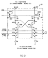
- FIG. 2 there is shown a schematic diagram of the memory cell 0,1 All other memory cells in array 200, other than those in the first row (i.e., cells 0,0; 1,0; 2,0; 3,0; 4,0), are identical to the memory cell 0,1 and therefore, only cell 0,1 will be described in detail.
- the transfer of a word to the cells can, if desired, be controlled by a single word line although two word lines are shown in Figure 2.
- memory cell 0,1 there is provided a pair of cross coupled multiple emitter Schottky transistors Q1 and Q2. Of importance, Schottky transistors need not be used, but the use of Schottky transistors provides greater speed.
- transistor Q1 there is provided a collector 201, a base 202 and three emitters 203, 204 and 205.
- transistor Q2 there is provided a collector 211, a base 212 and three emitters 213, 214 and 215.
- Coupling the collector 201 of transistor Q1 to the base 212 of transistor Q2 there is provided a 3K ohm resistor R1.
- the use of resistors R1 and R2 provides a greater voltage differential between the collectors 201 and 211 of transistors Q1 and Q2, respectively, thereby providing a greater tolerance, which in turn increases the yield of the devices.
- the transistor Q3 includes a collector 220, a base 221 and an emitter 222.
- the transistor Q4 includes a collector 223, a base 224 and an emitter 225.
- the collector 220 of transistor Q3 is coupled to the collector 201 of the transistor Q1.
- the collector 223 of the transistor Q4 is coupled to the collector 211 of the transistor Q2.
- the bases 221 and 224 of the transistors Q3 and Q4 are connected in common to a source of reference voltage VREF.
- the emitters 222 and 225 of the transistors Q3 and Q4 are connected in common to a source of potential, VCC.
- the collectors 201 and 211 of the transistors Q1 and Q2 are coupled to the corresponding second emitters 205 and 215 of the corresponding transistors Q1 and Q2 in the adjacent downstream word 0,2 (not shown) by the lines 101 and 102 respectively.
- the second emitters 205 and 215 of the memory cell 0,1 are coupled to the collectors 201 and 211 of the corresponding upstream memory cell 0,0 (not shown) by a pair of lines 101 and 102 respectively.
- All of the emitters 203 and 213 of the transistors Q1 and Q2 of each of the memory cells in a particular row of the array 200 are connected in common to the word line 3.
- the third emitters 204 and 214 in each of the memory cells in the row are connected in common to the word line 4.
- one of the two transistors Q1 and Q2 in each of the memory cells is conducting, thereby storing either a logical one (transistor Q1 on and transistor Q2 off) or a logical zero (transistor Q1 off and transistor Q2 on).
- a change in potential from a low to a high potential on both of the word lines 3 and 4 will cause the transistors Q1 and Q2 in cell 0,1 to either retain their present state of conduction or to switch between a conducting and a nonconducting state with the result that the downstream cell will contain the same data as the upstream cell.
- the potential on the collectors of the transistors Q1 and Q2 in an upstream memory cell and the state of conduction of the transistors in the downstream memory cell to which they are connected determines whether the transistors in the downstream memory cell switch between conducting and nonconducting states upon the application of predetermined word line control voltages to the latter transistors' first and second emitters.
- the data transfer operation is terminated when one or both of the word lines is brought low.
- Q1 and Q2 are assumed to be silicon bipolar Schottky transistors. All potentials are positive and are typical of the potentials used in the operation of silicon bipolar Schottky transistors.
- the lack of a change in the state of conduction of transistors Q1 and Q2 means that whatever logical value is stored by the upstream memory cell 0,0, is identical with the logical value stored by the memory cell 0,1. That is, if the upstream cell contained a logical "0" (or a logical "1") so does the memory cell 0,1 also stores a logical "0" (or a logical "1").
- the potentials assumed to exist on the second emitters 205, 215 of transistors Q1 and Q2 are reversed from those assumed in examples 1, 2 and 3. That is, the upstream cell 0,0 is assumed to contain a logical "1" and the cell 0,1 to be described contains a logical "0" with 1.2 and .6 volts on its second emitters 205 and 215 respectively.
- a further increase in the potential on the first emitters 203 and 213 from .6 to 1.1 volts results in switching the first emitter 203 and hence transistor Q1, from a conducting state to a nonconducting state.
- the second emitter 215 of transistor Q2 and, hence, the transistor Q2 is switched from a nonconducting to a conducting state.
- the logical one stored in upstream cell 0,0 is copied into cell 0,1.
- the reason why the transistors Q1 and Q2 switch states is because, as the potential on the collector of Q1 and, hence, on the base Q2 rises to a level whereat there is a .8 volt base-to-second emitter voltage for the second emitter 215 of Q2, the second emitter 215 begins conducting. As the second emitter 215 of Q2 begins conducting, the collector 211 potential thereof drops to .9 volts, i.e., .3 volts above the second emitter 215 potential of .6 volts.
- the potential on the collector 211 of Q2 drops to .9 volts, the potential on the base 202 of Q1 follows .1 volts below to a potential of .8 volts, thus turning off the first emitter 203 of the transistor Q1.
Landscapes
- Engineering & Computer Science (AREA)
- Theoretical Computer Science (AREA)
- Physics & Mathematics (AREA)
- General Engineering & Computer Science (AREA)
- General Physics & Mathematics (AREA)
- Static Random-Access Memory (AREA)
- Semiconductor Memories (AREA)
Applications Claiming Priority (2)
| Application Number | Priority Date | Filing Date | Title |
|---|---|---|---|
| US06/551,736 US4574367A (en) | 1983-11-10 | 1983-11-10 | Memory cell and array |
| US551736 | 1983-11-10 |
Publications (3)
| Publication Number | Publication Date |
|---|---|
| EP0142266A2 EP0142266A2 (en) | 1985-05-22 |
| EP0142266A3 EP0142266A3 (en) | 1987-07-01 |
| EP0142266B1 true EP0142266B1 (en) | 1993-12-29 |
Family
ID=24202465
Family Applications (1)
| Application Number | Title | Priority Date | Filing Date |
|---|---|---|---|
| EP84306928A Expired - Lifetime EP0142266B1 (en) | 1983-11-10 | 1984-10-10 | Memory Array |
Country Status (4)
| Country | Link |
|---|---|
| US (1) | US4574367A (https=) |
| EP (1) | EP0142266B1 (https=) |
| JP (1) | JPS60115093A (https=) |
| DE (2) | DE3486261T2 (https=) |
Families Citing this family (1)
| Publication number | Priority date | Publication date | Assignee | Title |
|---|---|---|---|---|
| US4922411A (en) * | 1988-12-27 | 1990-05-01 | Atmel Corporation | Memory cell circuit with supplemental current |
Family Cites Families (5)
| Publication number | Priority date | Publication date | Assignee | Title |
|---|---|---|---|---|
| US3487376A (en) * | 1965-12-29 | 1969-12-30 | Honeywell Inc | Plural emitter semiconductive storage device |
| US3764825A (en) * | 1972-01-10 | 1973-10-09 | R Stewart | Active element memory |
| SU752490A1 (ru) * | 1976-06-03 | 1980-07-30 | Предприятие П/Я В-8466 | Трехтактный регистр сдвига |
| US4151609A (en) * | 1977-10-11 | 1979-04-24 | Monolithic Memories, Inc. | First in first out (FIFO) memory |
| JPS5564685A (en) * | 1978-11-07 | 1980-05-15 | Fujitsu Ltd | Semiconductor memory unit |
-
1983
- 1983-11-10 US US06/551,736 patent/US4574367A/en not_active Expired - Lifetime
-
1984
- 1984-10-10 DE DE84306928T patent/DE3486261T2/de not_active Expired - Fee Related
- 1984-10-10 DE DE198484306928T patent/DE142266T1/de active Pending
- 1984-10-10 EP EP84306928A patent/EP0142266B1/en not_active Expired - Lifetime
- 1984-11-10 JP JP59236003A patent/JPS60115093A/ja active Granted
Also Published As
| Publication number | Publication date |
|---|---|
| JPH0430678B2 (https=) | 1992-05-22 |
| EP0142266A2 (en) | 1985-05-22 |
| DE142266T1 (de) | 1986-03-20 |
| JPS60115093A (ja) | 1985-06-21 |
| DE3486261D1 (de) | 1994-02-10 |
| EP0142266A3 (en) | 1987-07-01 |
| DE3486261T2 (de) | 1994-04-28 |
| US4574367A (en) | 1986-03-04 |
Similar Documents
| Publication | Publication Date | Title |
|---|---|---|
| US4125877A (en) | Dual port random access memory storage cell | |
| US4193127A (en) | Simultaneous read/write cell | |
| EP0024853B1 (en) | Semiconductor memory circuit including a hold current controlling circuit | |
| JP2003030980A (ja) | 半導体記憶装置 | |
| KR930000760B1 (ko) | 라인 전환 회로 및 그를 사용한 반도체 메모리 | |
| US4933905A (en) | Semiconductor memory device for reducing power dissipation during a write operation | |
| US4168539A (en) | Memory system with row clamping arrangement | |
| EP0142266B1 (en) | Memory Array | |
| EP0250930B1 (en) | Multiple rom data state, read/write memory cell | |
| US3551900A (en) | Information storage and decoder system | |
| US4035784A (en) | Asymmetrical memory cell arrangement | |
| US5508969A (en) | Adjacent row shift redundancy circuit having signal restorer coupled to programmable links | |
| US3588846A (en) | Storage cell with variable power level | |
| EP0357749B1 (en) | Bipolar ram with no write recovery time | |
| US4075690A (en) | Write enhancement circuit | |
| US4272811A (en) | Write and read control circuit for semiconductor memories | |
| US4506349A (en) | Cross-coupled transistor memory cell for MOS random access memory of reduced power dissipation | |
| EP0087919A2 (en) | A static type semiconductor memory device including a word line discharging circuit | |
| CA2109835C (en) | Differential latching inverter and random access memory using same | |
| EP0161514B1 (en) | Dual mode logic circuit | |
| KR20030063186A (ko) | 데이터 비트 기록 방법 및 회로 | |
| US4592023A (en) | Latch for storing a data bit and a store incorporating said latch | |
| EP0057556B1 (en) | Static semiconductor memory device | |
| EP0325344B1 (en) | Transfer circuit for signal lines | |
| EP0479274B1 (en) | Semiconductor memory device |
Legal Events
| Date | Code | Title | Description |
|---|---|---|---|
| PUAI | Public reference made under article 153(3) epc to a published international application that has entered the european phase |
Free format text: ORIGINAL CODE: 0009012 |
|
| AK | Designated contracting states |
Designated state(s): DE FR GB NL |
|
| TCNL | Nl: translation of patent claims filed | ||
| EL | Fr: translation of claims filed | ||
| DET | De: translation of patent claims | ||
| PUAL | Search report despatched |
Free format text: ORIGINAL CODE: 0009013 |
|
| AK | Designated contracting states |
Kind code of ref document: A3 Designated state(s): DE FR GB NL |
|
| 17P | Request for examination filed |
Effective date: 19871210 |
|
| RAP1 | Party data changed (applicant data changed or rights of an application transferred) |
Owner name: ADVANCED MICRO DEVICES, INC. |
|
| 17Q | First examination report despatched |
Effective date: 19890523 |
|
| GRAA | (expected) grant |
Free format text: ORIGINAL CODE: 0009210 |
|
| AK | Designated contracting states |
Kind code of ref document: B1 Designated state(s): DE FR GB NL |
|
| REF | Corresponds to: |
Ref document number: 3486261 Country of ref document: DE Date of ref document: 19940210 |
|
| ET | Fr: translation filed | ||
| PLBE | No opposition filed within time limit |
Free format text: ORIGINAL CODE: 0009261 |
|
| STAA | Information on the status of an ep patent application or granted ep patent |
Free format text: STATUS: NO OPPOSITION FILED WITHIN TIME LIMIT |
|
| 26N | No opposition filed | ||
| PGFP | Annual fee paid to national office [announced via postgrant information from national office to epo] |
Ref country code: DE Payment date: 20010330 Year of fee payment: 17 |
|
| PGFP | Annual fee paid to national office [announced via postgrant information from national office to epo] |
Ref country code: GB Payment date: 20010409 Year of fee payment: 17 |
|
| PGFP | Annual fee paid to national office [announced via postgrant information from national office to epo] |
Ref country code: FR Payment date: 20010427 Year of fee payment: 17 |
|
| PGFP | Annual fee paid to national office [announced via postgrant information from national office to epo] |
Ref country code: NL Payment date: 20010430 Year of fee payment: 17 |
|
| PG25 | Lapsed in a contracting state [announced via postgrant information from national office to epo] |
Ref country code: GB Free format text: LAPSE BECAUSE OF NON-PAYMENT OF DUE FEES Effective date: 20011010 |
|
| REG | Reference to a national code |
Ref country code: GB Ref legal event code: IF02 |
|
| PG25 | Lapsed in a contracting state [announced via postgrant information from national office to epo] |
Ref country code: NL Free format text: LAPSE BECAUSE OF NON-PAYMENT OF DUE FEES Effective date: 20020501 |
|
| GBPC | Gb: european patent ceased through non-payment of renewal fee |
Effective date: 20011010 |
|
| PG25 | Lapsed in a contracting state [announced via postgrant information from national office to epo] |
Ref country code: FR Free format text: LAPSE BECAUSE OF NON-PAYMENT OF DUE FEES Effective date: 20020628 |
|
| NLV4 | Nl: lapsed or anulled due to non-payment of the annual fee |
Effective date: 20020501 |
|
| PG25 | Lapsed in a contracting state [announced via postgrant information from national office to epo] |
Ref country code: DE Free format text: LAPSE BECAUSE OF NON-PAYMENT OF DUE FEES Effective date: 20020702 |
|
| REG | Reference to a national code |
Ref country code: FR Ref legal event code: ST |
|
| APAH | Appeal reference modified |
Free format text: ORIGINAL CODE: EPIDOSCREFNO |