EP0137563A2 - Umschaltungsverfahren mit automatischem Phasenausgleich der Daten über +/- 3,5 Bits und Vorrichtung zur Durchfürung des Verfahrens - Google Patents
Umschaltungsverfahren mit automatischem Phasenausgleich der Daten über +/- 3,5 Bits und Vorrichtung zur Durchfürung des Verfahrens Download PDFInfo
- Publication number
- EP0137563A2 EP0137563A2 EP84201411A EP84201411A EP0137563A2 EP 0137563 A2 EP0137563 A2 EP 0137563A2 EP 84201411 A EP84201411 A EP 84201411A EP 84201411 A EP84201411 A EP 84201411A EP 0137563 A2 EP0137563 A2 EP 0137563A2
- Authority
- EP
- European Patent Office
- Prior art keywords
- writing
- rhythm
- channel
- phase
- rhythms
- Prior art date
- Legal status (The legal status is an assumption and is not a legal conclusion. Google has not performed a legal analysis and makes no representation as to the accuracy of the status listed.)
- Granted
Links
Images
Classifications
-
- H—ELECTRICITY
- H04—ELECTRIC COMMUNICATION TECHNIQUE
- H04L—TRANSMISSION OF DIGITAL INFORMATION, e.g. TELEGRAPHIC COMMUNICATION
- H04L1/00—Arrangements for detecting or preventing errors in the information received
- H04L1/02—Arrangements for detecting or preventing errors in the information received by diversity reception
Definitions
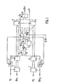
- the invention relates to a device ensuring the automatic correction of the relative position of the data signals transmitted on two channels carrying the same digital information but with a phase difference of up to a few bits, said correction being followed by switching of the lower quality channel. on the better quality channel, each of said channels being connected to the write input of a buffer memory and the write rhythms between each of said channels being re-phased by means of a phase locked loop.
- Such a device is capable of being used each time that the same digital information is routed according to two different channels in order to ensure greater security of the transmission.
- a coupler or separator directs information to the channels.
- external assessment criteria are transmitted to a Logic which determines the choice of the best quality channel; The problem is then to switch from one channel to the other without losing information.
- This device applies in particular in transmission by radio-relay systems in diversity reception systems based on the assumption of the low probability that two transmission channels will become defective simultaneously.
- the only backup channel common to the n normal channels conveys The information of the channel which becomes bad at a given time. When this channel becomes good again, the backup channel is released so that it can again temporarily replace another defective channel.
- the binary information processing units located downstream of the switching device (for example PABX if it is a telephone transmission) synchronize with the signal itself.
- the propagation times of the same information on two different transmission channels are not strictly identical; they present a difference depending on the conditions of ether crossing and all the greater the faster the speed of information (from 2 Mbits / s to 140 Mbits / s). This difference may be sufficient to introduce on reception an additional transition in the clock signal and a fluctuating offset of several bits between the information transmitted on the two channels.
- the message is truncated into a part transmitted on the first channel and into another part transmitted on the second channel. In the absence of precaution a discontinuity in the message is established since bits or bits have been deleted or added. It follows that the equipment located downstream has lost their synchronization. This defect results in the loss of a considerable amount of binary information.
- the subject of the present invention is a device making it possible to switch channels in a shorter time, without loss or without providing information on ⁇ 3.5 bits and which operates at the level of real data, ie at the output of the buffer memory, which makes it possible to achieve a simpler structure of this memory. It is thus more convenient to integrate the whole of the switching gate into a smaller pre-distributed circuit.
- the device according to the invention is remarkable in that the read output of said buffer memory is connected to an input of the switch on the data signals, the read rate being slaved to the write rate and out of phase with relation to the latter in order to ensure between the writing and the reading a sufficient time interval to effect the switching to the better quality channel and during which the writing rhythm of said better quality channel is increased, its reading rhythm remaining unchanged, so as to make up for a few bits
- the phase difference of said data signals between the two channels, the write information of each buffer memory being transmitted to a logic comparator which controls, according to the request of switching in progress, said write rhythms and the position of the switch on the data signals.
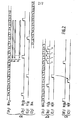
- two channels convey the same digital information at a given time, with however a phase difference of up to a few bits.
- FIGS. 2a and 2b are respectively the time diagrams relating to channels 2 and 1 in their initial state at the time of the switching request.
- FIG. 2c is the time diagram relating to channel 1 after switching.
- Channel 2 being assumed at the outset to be the one whose quality is degraded, it is proposed to switch to channel 1 whose quality is the best.
- the pace of Playing The voltage controlled oscillator is shown in Line C 1 always out of phase with respect to the rhythm H 2/8.
- the writing instant therefore moves by one bit at each writing (t 2 , t 3 %) by transferring the last 8 bits received.
- the write speed on channel 1 is maintained at H 1/7 throughout the research phase during which the evolution of data on channel 1 is the following:
- the delay or advance of this writing instant relative to the other must not exceed half the size of the buffer memory.
Applications Claiming Priority (2)
| Application Number | Priority Date | Filing Date | Title |
|---|---|---|---|
| FR8315989A FR2553244B1 (fr) | 1983-10-07 | 1983-10-07 | Dispositif de commutation avec remise en phase automatique des donnees sur 3,5 bits |
| FR8315989 | 1983-10-07 |
Publications (3)
| Publication Number | Publication Date |
|---|---|
| EP0137563A2 true EP0137563A2 (de) | 1985-04-17 |
| EP0137563A3 EP0137563A3 (en) | 1985-06-19 |
| EP0137563B1 EP0137563B1 (de) | 1989-01-04 |
Family
ID=9292927
Family Applications (1)
| Application Number | Title | Priority Date | Filing Date |
|---|---|---|---|
| EP84201411A Expired EP0137563B1 (de) | 1983-10-07 | 1984-10-04 | Umschaltungsverfahren mit automatischem Phasenausgleich der Daten über +/- 3,5 Bits und Vorrichtung zur Durchfürung des Verfahrens |
Country Status (6)
| Country | Link |
|---|---|
| US (1) | US4744095A (de) |
| EP (1) | EP0137563B1 (de) |
| JP (1) | JPS60121842A (de) |
| AU (1) | AU564860B2 (de) |
| DE (1) | DE3476005D1 (de) |
| FR (1) | FR2553244B1 (de) |
Cited By (4)
| Publication number | Priority date | Publication date | Assignee | Title |
|---|---|---|---|---|
| EP0260603A2 (de) * | 1986-09-11 | 1988-03-23 | Nec Corporation | Kanalumschaltungseinrichtung |
| EP0261601A2 (de) * | 1986-09-20 | 1988-03-30 | Fujitsu Limited | Kanalersatzschaltungssystem für ein Funkübertragungssystem von digitalen Daten |
| EP0454246A1 (de) * | 1990-04-27 | 1991-10-30 | T.R.T. Telecommunications Radioelectriques Et Telephoniques | Phasenkorrekturschaltung für Signale in einem System mit doppelten digitalen Leitungen |
| US5631927A (en) * | 1994-06-17 | 1997-05-20 | Lucent Technologies Inc. | Shifting circuit for a transmission system with multiple links |
Families Citing this family (6)
| Publication number | Priority date | Publication date | Assignee | Title |
|---|---|---|---|---|
| US5051979A (en) * | 1990-06-28 | 1991-09-24 | At&T Bell Laboratories | Method and apparatus for errorless switching |
| US5325405A (en) * | 1991-08-27 | 1994-06-28 | Motorola, Inc. | Burst mode receiver control |
| US5251210A (en) * | 1991-11-01 | 1993-10-05 | Ibm Corporation | Method and apparatus for transforming low bandwidth telecommunications channels into a high bandwidth telecommunication channel |
| US6647028B1 (en) | 1997-09-30 | 2003-11-11 | Cisco Technology, Inc. | System and method for recovering and restoring lost data in a N-channel coherent data transmission system |
| JP4359786B2 (ja) * | 2007-03-22 | 2009-11-04 | 日本電気株式会社 | データ伝送装置及びクロック切替回路 |
| US7929564B2 (en) * | 2008-03-14 | 2011-04-19 | Mediatek Inc. | System, apparatus, and method for loading bits into sub-channels |
Citations (5)
| Publication number | Priority date | Publication date | Assignee | Title |
|---|---|---|---|---|
| US4015205A (en) * | 1975-02-17 | 1977-03-29 | Nippon Electric Company, Ltd. | Baseband signal switching arrangement for diversity reception in a PCM radio communication system |
| FR2445669A1 (fr) * | 1978-12-26 | 1980-07-25 | Nippon Electric Co | Circuit de combinaison de signaux numeriques pour recepteur en diversite pour telecommunications numeriques |
| FR2462065A1 (fr) * | 1979-07-24 | 1981-02-06 | Thomson Csf | Dispositif de commutation automatique d'equipements de transmission de signaux numeriques et faisceaux hertziens comportant un tel dispositif |
| EP0060751A1 (de) * | 1981-03-13 | 1982-09-22 | Thomson-Csf | Einrichtung zur Umschaltung von Datenübertragungsstrecken |
| DE3206749A1 (de) * | 1982-02-25 | 1983-09-08 | Siemens AG, 1000 Berlin und 8000 München | Ersatzschaltung zum umschalten einer, ein digitalsignal fuehrende betriebsstrecke auf einer ersatzstrecke |
Family Cites Families (3)
| Publication number | Priority date | Publication date | Assignee | Title |
|---|---|---|---|---|
| JPS5439093B2 (de) * | 1974-08-24 | 1979-11-26 | ||
| US4349914A (en) * | 1980-04-01 | 1982-09-14 | Ford Aerospace & Communications Corp. | Bit synchronous switching system for space diversity operation |
| US4417348A (en) * | 1981-04-30 | 1983-11-22 | Bell Telephone Laboratories, Incorporated | Errorless line protection switcher |
-
1983
- 1983-10-07 FR FR8315989A patent/FR2553244B1/fr not_active Expired
-
1984
- 1984-10-04 EP EP84201411A patent/EP0137563B1/de not_active Expired
- 1984-10-04 DE DE8484201411T patent/DE3476005D1/de not_active Expired
- 1984-10-05 JP JP59209586A patent/JPS60121842A/ja active Pending
- 1984-10-05 AU AU33865/84A patent/AU564860B2/en not_active Ceased
-
1986
- 1986-08-11 US US06/895,528 patent/US4744095A/en not_active Expired - Fee Related
Patent Citations (5)
| Publication number | Priority date | Publication date | Assignee | Title |
|---|---|---|---|---|
| US4015205A (en) * | 1975-02-17 | 1977-03-29 | Nippon Electric Company, Ltd. | Baseband signal switching arrangement for diversity reception in a PCM radio communication system |
| FR2445669A1 (fr) * | 1978-12-26 | 1980-07-25 | Nippon Electric Co | Circuit de combinaison de signaux numeriques pour recepteur en diversite pour telecommunications numeriques |
| FR2462065A1 (fr) * | 1979-07-24 | 1981-02-06 | Thomson Csf | Dispositif de commutation automatique d'equipements de transmission de signaux numeriques et faisceaux hertziens comportant un tel dispositif |
| EP0060751A1 (de) * | 1981-03-13 | 1982-09-22 | Thomson-Csf | Einrichtung zur Umschaltung von Datenübertragungsstrecken |
| DE3206749A1 (de) * | 1982-02-25 | 1983-09-08 | Siemens AG, 1000 Berlin und 8000 München | Ersatzschaltung zum umschalten einer, ein digitalsignal fuehrende betriebsstrecke auf einer ersatzstrecke |
Cited By (7)
| Publication number | Priority date | Publication date | Assignee | Title |
|---|---|---|---|---|
| EP0260603A2 (de) * | 1986-09-11 | 1988-03-23 | Nec Corporation | Kanalumschaltungseinrichtung |
| EP0260603A3 (en) * | 1986-09-11 | 1989-06-28 | Nec Corporation | Channel switching system |
| EP0261601A2 (de) * | 1986-09-20 | 1988-03-30 | Fujitsu Limited | Kanalersatzschaltungssystem für ein Funkübertragungssystem von digitalen Daten |
| EP0261601A3 (en) * | 1986-09-20 | 1989-07-05 | Fujitsu Limited | Channel-system exchange system for digital data radio-communication system |
| EP0454246A1 (de) * | 1990-04-27 | 1991-10-30 | T.R.T. Telecommunications Radioelectriques Et Telephoniques | Phasenkorrekturschaltung für Signale in einem System mit doppelten digitalen Leitungen |
| FR2661579A1 (fr) * | 1990-04-27 | 1991-10-31 | Trt Telecom Radio Electr | Dispositif de mise en phase de signaux dans un systeme a doublement du conduit numerique. |
| US5631927A (en) * | 1994-06-17 | 1997-05-20 | Lucent Technologies Inc. | Shifting circuit for a transmission system with multiple links |
Also Published As
| Publication number | Publication date |
|---|---|
| US4744095A (en) | 1988-05-10 |
| EP0137563A3 (en) | 1985-06-19 |
| FR2553244A1 (fr) | 1985-04-12 |
| AU3386584A (en) | 1985-04-18 |
| EP0137563B1 (de) | 1989-01-04 |
| AU564860B2 (en) | 1987-08-27 |
| JPS60121842A (ja) | 1985-06-29 |
| FR2553244B1 (fr) | 1988-12-30 |
| DE3476005D1 (en) | 1989-02-09 |
Similar Documents
| Publication | Publication Date | Title |
|---|---|---|
| CA1240061A (fr) | Dispositifs de synchronisation de trame | |
| FR2466837A1 (fr) | Memoire tampon d'interface terrestre a acces multiples par repartition de temps pour operations entrelacees | |
| FR2590099A1 (fr) | Procede pour transmettre une image de haute definition par un canal de communication a bande etroite | |
| EP0137563A2 (de) | Umschaltungsverfahren mit automatischem Phasenausgleich der Daten über +/- 3,5 Bits und Vorrichtung zur Durchfürung des Verfahrens | |
| FR2505109A1 (fr) | Systeme de transmission numerique avec possibilite de commutation sur un canal de protection | |
| EP0037299B1 (de) | Synchronisierungsanordnung für blockweise übertragene digitale Nachrichten | |
| EP0167773B1 (de) | Verfahren zum Übertragen und Empfangen hochwertiger Tonprogramme und Empfängereinrichtung | |
| EP0249930B1 (de) | Verfahren zur Synchronisation von zwei binären Strömen | |
| FR2529040A1 (fr) | Systeme de radiocommunications a sauts de frequence, a redondance inter-paliers | |
| EP0454246B1 (de) | Phasenkorrekturschaltung für Signale in einem System mit doppelten digitalen Leitungen | |
| EP0064923B1 (de) | System zur Phasensynchronisation digitaler Datenströme und seine Verwendung bei der Umschaltung der Datenströme | |
| CH640678A5 (fr) | Procede et installation de transmission simultanee d'une onde basse frequence et d'un signal numerique mic. | |
| EP0231711A1 (de) | Verfahren und Multiplexier-Demultiplexier-Einrichtungen zur Qualitätsmessung und Fehlerlokalisierung in multiplexierten digitalen Kanälen | |
| EP0242915A1 (de) | Einrichtung zur Taktwiedergewinnung für ein Nachrichtenübertragungssystem, welche in einer Übertragungsrichtung mit dem Vielfachzugriff im Zeitmultiplexprinzip arbeitet | |
| FR2658969A1 (fr) | Systeme constitue en reseau tel qu'un systeme radiotelephonique cellulaire, permettant de mesurer le retard de transmission entre nóoeuds du reseau et de les synchroniser entre eux. | |
| EP0013341A1 (de) | System zur Zeitkompression von Sprachsignalen | |
| EP0060751B1 (de) | Einrichtung zur Umschaltung von Datenübertragungsstrecken | |
| FR2562745A1 (fr) | Systeme de synchronisation d'onde porteuse et station de base convenant pour ce systeme | |
| FR2462065A1 (fr) | Dispositif de commutation automatique d'equipements de transmission de signaux numeriques et faisceaux hertziens comportant un tel dispositif | |
| EP0396461A1 (de) | Anordnung zur Synchronisation eines pseudobinären Signals mit einem durch Phasensprung regenerierten Taktsignal | |
| EP0016678B1 (de) | Bittaktrückgewinnungs-Vorrichtung | |
| FR2710804A1 (fr) | Dispositif numérique de connexion d'une pluralité de stations de travail sur un réseau local en anneau. | |
| EP0469996B1 (de) | Verfahren und Einrichtung zur Adaptation eines Signals, welches zwischen zwei digitalen Netzwerken übermittelt wird | |
| FR2579047A1 (fr) | Procede de synchronisation par rattrapage de frequence et dispositif de mise en oeuvre du procede | |
| FR2793623A1 (fr) | Procede et dispositif de controle de la synchronisation entre deux noeuds ni-1, ni d'un reseau |
Legal Events
| Date | Code | Title | Description |
|---|---|---|---|
| PUAI | Public reference made under article 153(3) epc to a published international application that has entered the european phase |
Free format text: ORIGINAL CODE: 0009012 |
|
| AK | Designated contracting states |
Designated state(s): DE FR GB IT SE |
|
| PUAL | Search report despatched |
Free format text: ORIGINAL CODE: 0009013 |
|
| RTI1 | Title (correction) | ||
| AK | Designated contracting states |
Designated state(s): DE FR GB IT SE |
|
| 111L | Licence recorded |
Free format text: 0100 L'ETAT - ADMINISTRATION DES P.T.T. - CENTRE NATIONAL D'ETUDES DES TELECOMMUNICATIONS |
|
| 17P | Request for examination filed |
Effective date: 19851218 |
|
| 17Q | First examination report despatched |
Effective date: 19870225 |
|
| GRAA | (expected) grant |
Free format text: ORIGINAL CODE: 0009210 |
|
| AK | Designated contracting states |
Kind code of ref document: B1 Designated state(s): DE FR GB IT SE |
|
| REF | Corresponds to: |
Ref document number: 3476005 Country of ref document: DE Date of ref document: 19890209 |
|
| ITF | It: translation for a ep patent filed |
Owner name: ING. C. GREGORJ S.P.A. |
|
| GBT | Gb: translation of ep patent filed (gb section 77(6)(a)/1977) | ||
| PLBE | No opposition filed within time limit |
Free format text: ORIGINAL CODE: 0009261 |
|
| STAA | Information on the status of an ep patent application or granted ep patent |
Free format text: STATUS: NO OPPOSITION FILED WITHIN TIME LIMIT |
|
| 26N | No opposition filed | ||
| REG | Reference to a national code |
Ref country code: FR Ref legal event code: TP |
|
| ITTA | It: last paid annual fee | ||
| ITPR | It: changes in ownership of a european patent |
Owner name: CESSIONE;TRT TELECOMMUNICATIONS RADIOELECTRIQUES E |
|
| REG | Reference to a national code |
Ref country code: GB Ref legal event code: 732E |
|
| EAL | Se: european patent in force in sweden |
Ref document number: 84201411.0 |
|
| REG | Reference to a national code |
Ref country code: FR Ref legal event code: TP |
|
| REG | Reference to a national code |
Ref country code: GB Ref legal event code: 732E |
|
| PGFP | Annual fee paid to national office [announced via postgrant information from national office to epo] |
Ref country code: GB Payment date: 19960930 Year of fee payment: 13 |
|
| PGFP | Annual fee paid to national office [announced via postgrant information from national office to epo] |
Ref country code: FR Payment date: 19961022 Year of fee payment: 13 |
|
| PGFP | Annual fee paid to national office [announced via postgrant information from national office to epo] |
Ref country code: SE Payment date: 19961025 Year of fee payment: 13 |
|
| PGFP | Annual fee paid to national office [announced via postgrant information from national office to epo] |
Ref country code: DE Payment date: 19961218 Year of fee payment: 13 |
|
| REG | Reference to a national code |
Ref country code: FR Ref legal event code: TP |
|
| PG25 | Lapsed in a contracting state [announced via postgrant information from national office to epo] |
Ref country code: GB Free format text: LAPSE BECAUSE OF NON-PAYMENT OF DUE FEES Effective date: 19971004 |
|
| PG25 | Lapsed in a contracting state [announced via postgrant information from national office to epo] |
Ref country code: SE Free format text: LAPSE BECAUSE OF NON-PAYMENT OF DUE FEES Effective date: 19971005 |
|
| PG25 | Lapsed in a contracting state [announced via postgrant information from national office to epo] |
Ref country code: FR Free format text: THE PATENT HAS BEEN ANNULLED BY A DECISION OF A NATIONAL AUTHORITY Effective date: 19971031 |
|
| GBPC | Gb: european patent ceased through non-payment of renewal fee |
Effective date: 19971004 |
|
| PG25 | Lapsed in a contracting state [announced via postgrant information from national office to epo] |
Ref country code: DE Free format text: LAPSE BECAUSE OF NON-PAYMENT OF DUE FEES Effective date: 19980701 |
|
| EUG | Se: european patent has lapsed |
Ref document number: 84201411.0 |
|
| REG | Reference to a national code |
Ref country code: FR Ref legal event code: ST |