EP0137563A2 - Switching method with automatic data phase resetting over +/- 3.5 bitsand device for carrying out said method - Google Patents
Switching method with automatic data phase resetting over +/- 3.5 bitsand device for carrying out said method Download PDFInfo
- Publication number
- EP0137563A2 EP0137563A2 EP84201411A EP84201411A EP0137563A2 EP 0137563 A2 EP0137563 A2 EP 0137563A2 EP 84201411 A EP84201411 A EP 84201411A EP 84201411 A EP84201411 A EP 84201411A EP 0137563 A2 EP0137563 A2 EP 0137563A2
- Authority
- EP
- European Patent Office
- Prior art keywords
- writing
- rhythm
- channel
- phase
- rhythms
- Prior art date
- Legal status (The legal status is an assumption and is not a legal conclusion. Google has not performed a legal analysis and makes no representation as to the accuracy of the status listed.)
- Granted
Links
Images
Classifications
-
- H—ELECTRICITY
- H04—ELECTRIC COMMUNICATION TECHNIQUE
- H04L—TRANSMISSION OF DIGITAL INFORMATION, e.g. TELEGRAPHIC COMMUNICATION
- H04L1/00—Arrangements for detecting or preventing errors in the information received
- H04L1/02—Arrangements for detecting or preventing errors in the information received by diversity reception
Definitions
- the invention relates to a device ensuring the automatic correction of the relative position of the data signals transmitted on two channels carrying the same digital information but with a phase difference of up to a few bits, said correction being followed by switching of the lower quality channel. on the better quality channel, each of said channels being connected to the write input of a buffer memory and the write rhythms between each of said channels being re-phased by means of a phase locked loop.
- Such a device is capable of being used each time that the same digital information is routed according to two different channels in order to ensure greater security of the transmission.
- a coupler or separator directs information to the channels.
- external assessment criteria are transmitted to a Logic which determines the choice of the best quality channel; The problem is then to switch from one channel to the other without losing information.
- This device applies in particular in transmission by radio-relay systems in diversity reception systems based on the assumption of the low probability that two transmission channels will become defective simultaneously.
- the only backup channel common to the n normal channels conveys The information of the channel which becomes bad at a given time. When this channel becomes good again, the backup channel is released so that it can again temporarily replace another defective channel.
- the binary information processing units located downstream of the switching device (for example PABX if it is a telephone transmission) synchronize with the signal itself.
- the propagation times of the same information on two different transmission channels are not strictly identical; they present a difference depending on the conditions of ether crossing and all the greater the faster the speed of information (from 2 Mbits / s to 140 Mbits / s). This difference may be sufficient to introduce on reception an additional transition in the clock signal and a fluctuating offset of several bits between the information transmitted on the two channels.
- the message is truncated into a part transmitted on the first channel and into another part transmitted on the second channel. In the absence of precaution a discontinuity in the message is established since bits or bits have been deleted or added. It follows that the equipment located downstream has lost their synchronization. This defect results in the loss of a considerable amount of binary information.
- the subject of the present invention is a device making it possible to switch channels in a shorter time, without loss or without providing information on ⁇ 3.5 bits and which operates at the level of real data, ie at the output of the buffer memory, which makes it possible to achieve a simpler structure of this memory. It is thus more convenient to integrate the whole of the switching gate into a smaller pre-distributed circuit.
- the device according to the invention is remarkable in that the read output of said buffer memory is connected to an input of the switch on the data signals, the read rate being slaved to the write rate and out of phase with relation to the latter in order to ensure between the writing and the reading a sufficient time interval to effect the switching to the better quality channel and during which the writing rhythm of said better quality channel is increased, its reading rhythm remaining unchanged, so as to make up for a few bits
- the phase difference of said data signals between the two channels, the write information of each buffer memory being transmitted to a logic comparator which controls, according to the request of switching in progress, said write rhythms and the position of the switch on the data signals.
- two channels convey the same digital information at a given time, with however a phase difference of up to a few bits.
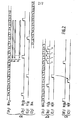
- FIGS. 2a and 2b are respectively the time diagrams relating to channels 2 and 1 in their initial state at the time of the switching request.
- FIG. 2c is the time diagram relating to channel 1 after switching.
- Channel 2 being assumed at the outset to be the one whose quality is degraded, it is proposed to switch to channel 1 whose quality is the best.
- the pace of Playing The voltage controlled oscillator is shown in Line C 1 always out of phase with respect to the rhythm H 2/8.
- the writing instant therefore moves by one bit at each writing (t 2 , t 3 %) by transferring the last 8 bits received.
- the write speed on channel 1 is maintained at H 1/7 throughout the research phase during which the evolution of data on channel 1 is the following:
- the delay or advance of this writing instant relative to the other must not exceed half the size of the buffer memory.
Abstract
Dispositif assurant la commutation de deux canaux véhiculant la même information numérique avec remise en phase automatique des données sur ±3,5 bits et comportant sur chaque canal un ensemble mémoire tampon (1, 2, 4) au rythme d'écriture Hi/Ni, un oscillateur (6) au rythme H assurant la lecture des mémoires tampon au rythme H/N et asservi en opposition de phase sur l'un ou l'autre des rythmes d'écriture, un comparateur logique (10) commandant les rythmes d'écriture Hi/Ni, l'aiguillage (8) des rythmes à l'entrée de l'oscillateur et le commutateur (5) sur les données. Dans la mémoire tampon du canal 2 supposé au départ comme étant celui dont la qualité se dégrade, les données sont converties en N trains parallèles au rythme H2/N et relues au rythme H/N de l'oscillateur. Sur le canal 1, dont la qualité est la meilleure, la fonction mémoire tampon est forcée en écriture au rythme H1/N - 1, le rythme de lecture restant inchangé, jusqu'à la coïncidence des N bits sur les deux canaux suivie de la commutation des données, du verrouillage du rythme d'écriture H1/N et de la commutation vers l'oscillateur du rythme H1/N. Application: transmission des données.Device ensuring the switching of two channels conveying the same digital information with automatic resetting of data on ± 3.5 bits and comprising on each channel a buffer memory unit (1, 2, 4) at the Hi / Ni writing rate, an oscillator (6) at rhythm H ensuring the reading of the buffer memories at rhythm H / N and controlled in phase opposition on one or other of the writing rhythms, a logic comparator (10) controlling the rhythms of Hi / Ni writing, the routing (8) of the rhythms at the input of the oscillator and the switch (5) on the data. In the buffer memory of channel 2 initially assumed to be the one whose quality is degraded, the data is converted into N trains parallel to the H2 / N rhythm and read again at the H / N rhythm of the oscillator. On channel 1, the best quality of which, the buffer memory function is forced to write at the rate H1 / N - 1, the reading rate remaining unchanged, until the N bits coincide on the two channels followed by the switching data, locking the H1 / N write rhythm and switching to the H1 / N rhythm oscillator. Application: data transmission.
Description
L'invention concerne un dispositif assurant la correction automatique de La position relative des signaux de données transmis sur deux canaux véhiculant la même information numérique mais avec un écart de phase pouvant atteindre quelques bits, Ladite correction étant suivie de la commutation du canal de moindre qualité sur Le canal de meilleure qualité, chacun desdits canaux étant relié à L'entrée d'écriture d'une mémoire tampon et Les rythmes d'écriture entre chacun desdits canaux étant remis en phase au moyen d'une boucle à verrouillage de phase.The invention relates to a device ensuring the automatic correction of the relative position of the data signals transmitted on two channels carrying the same digital information but with a phase difference of up to a few bits, said correction being followed by switching of the lower quality channel. on the better quality channel, each of said channels being connected to the write input of a buffer memory and the write rhythms between each of said channels being re-phased by means of a phase locked loop.
Un tel dispositif est susceptible d'être utilisé chaque fois qu'une même information numérique est acheminée suivant deux canaux différents afin d'assurer une plus grande sécurité de La transmission.Such a device is capable of being used each time that the same digital information is routed according to two different channels in order to ensure greater security of the transmission.
A L'émission, un coupleur ou un séparateur aiguille L'information vers Les canaux. A La réception, des critères d'appréciation extérieurs sont transmis à une Logique qui détermine le choix du canal de meilleure qualité ; Le problème est alors d'effectuer une commutation d'un canal sur L'autre sans perte d'information.On transmission, a coupler or separator directs information to the channels. At reception, external assessment criteria are transmitted to a Logic which determines the choice of the best quality channel; The problem is then to switch from one channel to the other without losing information.
Ce dispositif s'applique en particulier en transmission par faisceaux hertziens dans Les systèmes de réception en diversité basés sur L'hypothèse de la faible probabilité qu'ont deux canaux de transmission de devenir simultanément défectueux. L'unique canal de secours commun aux n canaux normaux (n étant habituellement égal à 7) véhicule L'information du canal qui devient mauvais à un instant donné. Lorsque ce canal redevient bon, Le canal de secours est Libéré pour qu'il puisse à nouveau se substituer temporairement à un autre canal défectueux.This device applies in particular in transmission by radio-relay systems in diversity reception systems based on the assumption of the low probability that two transmission channels will become defective simultaneously. The only backup channel common to the n normal channels (n being usually equal to 7) conveys The information of the channel which becomes bad at a given time. When this channel becomes good again, the backup channel is released so that it can again temporarily replace another defective channel.
Les organes de traitement de L'information binaire situés en aval du dispositif de commutation (par exemple Les autocommutateurs s'iL s'agit d'une transmission téléphonique) se synchronisent sur Le signal Lui-même. Mais Les temps de propagation d'une même information sur deux canaux de transmission différents ne sont pas rigoureusement identiques ; ils présentent un écart dépendant des conditions de traversée de L'éther et d'autant plus grand que le débit de L'information (de 2 Mbits/s à 140 Mbits/s) est plus rapide. Cet écart peut être suffisant pour introduire à La réception une transition supplémentaire dans Le signal d'horloge et un décalage fluctuant de plusieurs bits entre Les informations transmises sur Les deux canaux. A L'instant de La commutation d'un canal sur L'autre, le message est tronqué en une partie transmise sur le premier canal et en une autre partie transmise sur le second canal. En L'absence de précaution il s'établit une discontinuité dans le message puisqu'on a supprimé ou rajouté des bits. IL en résulte que Les matériels situés en aval ont perdu Leur synchronisation. Ce défaut entraîne La perte d'un nombre considérable d'informations binaires.The binary information processing units located downstream of the switching device (for example PABX if it is a telephone transmission) synchronize with the signal itself. However, the propagation times of the same information on two different transmission channels are not strictly identical; they present a difference depending on the conditions of ether crossing and all the greater the faster the speed of information (from 2 Mbits / s to 140 Mbits / s). This difference may be sufficient to introduce on reception an additional transition in the clock signal and a fluctuating offset of several bits between the information transmitted on the two channels. At the instant of switching from one channel to the other, the message is truncated into a part transmitted on the first channel and into another part transmitted on the second channel. In the absence of precaution a discontinuity in the message is established since bits or bits have been deleted or added. It follows that the equipment located downstream has lost their synchronization. This defect results in the loss of a considerable amount of binary information.
Afin de pallier ces inconvénients, divers dispositifs de commutation de canaux ont été proposés, par exemple celui décrit dans La demande de brevet européen n° 0 060 751 et qui comporte entre autres La mémoire tampon associée à chacun des canaux mentionnée dans Le préambule. Dans ce dispositif, La durée des données transmises est allongée dans un rapport n avant L'opération de commutation d'un canal sur L'autre qui a donc Lieu au niveau des données fictives, c'est-à-dire des données dont La durée est n fois plus Longue que celle des données réelles. IL en résulte une structure de mémoire tampon relativement complexe. De plus, au niveau des ordres de déphasage, Le comptage des divergences s'opère au moyen d'une fenêtre de mesure obtenue par un monostable et qui fixe un certain délai pour déphaser de 2π/n.In order to overcome these drawbacks, various channel switching devices have been proposed, for example that described in European patent application No. 0 060 751 and which comprises inter alia the buffer memory associated with each of the channels mentioned in the preamble. In this device, the duration of the transmitted data is extended in a report n before The operation of switching from one channel to the other which therefore takes place at the level of fictitious data, that is to say data whose duration is n times longer than that of the data real. This results in a relatively complex buffer structure. In addition, at the phase shift orders, the divergences are counted by means of a measurement window obtained by a monostable and which fixes a certain delay for phase shifting by 2π / n.
La présente invention a pour objet un dispositif permettant d'effectuer une commutation de canaux dans un délai plus court, sans perte ou sans apport d'information sur ± 3,5 bits et qui s'opère au niveau des données réelles c'est-à-dire en sortie de la mémoire tampon, ce qui permet de réaliser une structure plus simple de cette mémoire. IL est ainsi plus commode d'intégrer l'ensemble de La porte de commutation dans un circuit prédiffusé de plus petite taille.The subject of the present invention is a device making it possible to switch channels in a shorter time, without loss or without providing information on ± 3.5 bits and which operates at the level of real data, ie at the output of the buffer memory, which makes it possible to achieve a simpler structure of this memory. It is thus more convenient to integrate the whole of the switching gate into a smaller pre-distributed circuit.
A cet effet Le dispositif conforme à L'invention est remarquable en ce que la sortie de Lecture de ladite mémoire tampon est reliée à une entrée du commutateur sur Les signaux de données, le rythme de Lecture étant asservi au rythme d'écriture et déphasé par rapport à ce dernier afin d'assurer entre L'écriture et La Lecture un intervalle de temps suffisant pour effectuer La commutation sur le canal de meilleure qualité et pendant LequeL Le rythme d'écriture dudit canal de meilleure qualité est accru, son rythme de Lecture restant inchangé, de façon à rattraper sur quelques bits L'écart de phase desdits signaux de données entre Les deux canaux, Les informations d'écriture de chaque mémoire tampon étant transmises à un comparateur Logique qui commande, selon La demande de commutation en cours, lesdits rythmes d'écriture et La position du commutateur sur Les signaux de données.To this end, the device according to the invention is remarkable in that the read output of said buffer memory is connected to an input of the switch on the data signals, the read rate being slaved to the write rate and out of phase with relation to the latter in order to ensure between the writing and the reading a sufficient time interval to effect the switching to the better quality channel and during which the writing rhythm of said better quality channel is increased, its reading rhythm remaining unchanged, so as to make up for a few bits The phase difference of said data signals between the two channels, the write information of each buffer memory being transmitted to a logic comparator which controls, according to the request of switching in progress, said write rhythms and the position of the switch on the data signals.
La description suivante en regard des dessins annexés, Le tout donné à titre d'exemple fera bien comprendre comment L'invention peut être réalisée.
- La figure 1 est un schéma sous forme de blocs du dispositif de commutation selon un mode de réalisation de La présente invention.
- La figure 2 est un diagramme de temps représentant plusieurs signaux qui apparaissent dans le circuit de commutation conforme à L'invention.
- Figure 1 is a block diagram of the switching device according to an embodiment of the present invention.
- FIG. 2 is a time diagram representing several signals which appear in the switching circuit according to the invention.
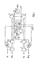
Sur Le schéma synoptique de La figure 1, deux canaux véhiculent à un moment donné La même information numérique avec toutefois un écart de phase pouvant atteindre quelques bits. Chaque canal est porteur d'un train binaire Bin, avec i = 1 pour l'un des canaux et i = 2 pour L'autre. Des critères extérieurs au dispositif conduisent à déterminer Le canal de meilleure qualité.In the block diagram of FIG. 1, two channels convey the same digital information at a given time, with however a phase difference of up to a few bits. Each channel carries a binary train Bin, with i = 1 for one of the channels and i = 2 for the other. Criteria external to the device lead to determining the best quality channel.
Le dispositif permettant d'effectuer La commutation d'un canal sur L'autre sans perte d'information est constitué par :
- 1° un dispositif mémoire tampon sur chacun des deux canaux. Ce dispositif comporte les registres 1 et 2 qui effectuent une conversion série parallèle sur Ni bits. A cet effet, les registres 1 et 2 reçoivent respectivement le signal d'horloge Hi de L'information binaire Bin, et à travers Le
diviseur 3, Le même signal d'horloge divisé par Ni. Les Ni bits en parallèle au rythme d'écriture Hi/Ni sont transmis à L'entrée d'unregistre 4 dans LequeL s'effectue une transformation parallèle série pour la lecture de l'information binaire Bin à travers L'aiguiLLage 5, l'ensemble desregistres 1, 2 et 4 formant ladite mémoire tampon. - 2° une boucle à verrouillage de phase commune aux deux canaux et constituée par un oscillateur contrôlé en
tension 6 au rythme H, dont La sortie est reliée auxregistres 4 et L'entrée à un mélangeur 7 qui reçoit par ailleurs à travers l'aiguillage 8 le signal d'horloge Hi divisé par Ni et Le signal H divisé par N à travers Le diviseur 9. On obtient ainsi selon l'invention L'asservissement en opposition de phase de l'oscillateur sur l'un ou L'autre des rythmes d'é.criture et la Lecture de La mémoire tampon au rythme H/N. - 3° un comparateur Logique 10 qui commande :
- - les rythmes d'écriture Hi/Ni pouvant être éventuellement forcés à Hi/Ni - 1,
- - l'aiguillage 8 des rythmes à L'entrée de La boucle à verrouillage de phase par le signal S1,
- - l'aiguillage 5 sur les données par le signal 52.
- 1 ° a buffer memory device on each of the two channels. This device includes
registers 1 and 2 which perform a parallel serial conversion on N i bits. To this end, theregisters 1 and 2 respectively receive the clock signal H i of the binary information Bin, and through thedivider 3, the same clock signal divided by N i . The N i bits in parallel with the writing rate H i / N i are transmitted to the entry of aregister 4 in LequeL a serial parallel transformation is carried out for the reading of the binary information Bin through the needle 5, the set ofregisters - 2 ° a phase locked loop common to the two channels and constituted by a voltage controlled
oscillator 6 at rhythm H, the output of which is connected toregisters 4 and the input to a mixer 7 which also receives through theswitch 8 the clock signal H i divided by N i and the signal H divided by N through Le divider 9. According to the invention, the servo in phase opposition of the oscillator is obtained in this way on one or the other of the writing rhythms and the reading of the buffer memory at the H / N rhythm. - 3 ° a Logic comparator 10 which controls:
- - the writing rhythms H i / N i can possibly be forced to H i / N i - 1,
- - the
routing 8 of the rhythms at the entry of the phase-locked loop by the signal S 1 , - - the switch 5 on the data by the signal 5 2 .
Ces ordres sont exécutés selon La demande de commutation en cours D et les informations d'écriture de chaque mémoire tampon transmises au comparateur 10.These orders are executed according to the current switching request D and the write information of each buffer memory transmitted to the comparator 10.
Le fonctionnement du circuit de commutation selon Le mode de réalisation de La présente invention sera décrit en Liaison avec Les diagrammes de temps de La figure 2.The operation of the switching circuit according to the embodiment of the present invention will be described in connection with the time diagrams of FIG. 2.
Les figures 2a et 2b sont respectivement Les diagrammes de temps relatifs aux canaux 2 et 1 dans leur état initial au moment de La demande de commutation.FIGS. 2a and 2b are respectively the time diagrams relating to
La figure 2c est Le diagramme de temps relatif au canal 1 après commutation.FIG. 2c is the time diagram relating to channel 1 after switching.
Le canal 2 étant supposé au départ comme étant celui dont La qualité se dégrade, on se propose d'effectuer la commutation sur Le canal 1 dont La qualité est La meilleure.Channel 2 being assumed at the outset to be the one whose quality is degraded, it is proposed to switch to channel 1 whose quality is the best.
Sur La figure 2a, La ligne A2 montre les données du canal 2, ... a-1, b-1,...h-1, ao, bo,...ho, a1, b1,...h1,... convertis dans la mémoire tampon en 8 trains parallèles (N2 = 8) au rythme d'écriture H2/8 représenté sur La ligne B2. La ligne C2 représente le rythme de lecture H/8 (N = 8) de l'oscillateur contrôlé en tension synchronisé en opposition de phase avec Le rythme d'écriture H2/8 du canal 2. La Ligne D2 montre les données du canal 2 relues au rythme H/8 = H2/8.In Figure 2a, Line A 2 shows the data for
On suppose que Les données du canal 1 représentées sur La ligne A1 de La figure 2b ont à L'instant d'écriture to une avance de phase de 1 bit sur celles du canal 2 et que le rythme d'écriture H1/8 (N1 = 8) représenté sur La Ligne B1 de La même figure a un retard de phase de 3 bits sur Le rythme d'écriture H2/8.It is assumed that the data of channel 1 represented on line A 1 of FIG. 2b have, at the time of writing t o, a phase advance of 1 bit over that of
Le rythme de Lecture de L'osciLLateur contrôlé en tension est représenté sur La Ligne C1 toujours en opposition de phase par rapport au rythme H2/8.The pace of Playing The voltage controlled oscillator is shown in Line C 1 always out of phase with respect to the rhythm H 2/8.
Lors de La demande de commutation du canal 2 vers Le canal 1, La fonction mémoire tampon du canal 1 est forcée à L'instant d'écriture t1 au rythme d'écriture H1/7 suivant La représentation en pointillés de La figure, Le rythme de lecture restant inchangé.When the channel switching
L'instant d'écriture se déplace donc d'un bit à chaque écriture (t2, t3...) en transférant Les 8 derniers bits reçus. Dans ce cas, il y a nécessairement une position parmi Les 8 possibles qui entraîne une coïncidence des 8 bits entre les sorties des deux mémoires tampon.The writing instant therefore moves by one bit at each writing (t 2 , t 3 ...) by transferring the last 8 bits received. In this case, there is necessarily a position among the 8 possible which results in a coincidence of the 8 bits between the outputs of the two buffer memories.
Cette coïncidence qui a Lieu si L'instant d'écriture dans La mémoire 1 apparaît sur Le même bit que celui pour lequel L'instant d'écriture apparaît dans La mémoire 2 se produit après un décalage de 3 bits dans Le cas représenté sur La figure 2.This coincidence which takes place if the instant of writing in memory 1 appears on the same bit as that for which the instant of writing appears in
Le rythme d'écriture sur le canal 1 est maintenu à H1/7 pendant toute la phase de recherche durant LaqueLLe l'évolution des données sur le canal 1 est La suivante :

Il faut par ailleurs que Le retard ou l'avance de cet instant d'écriture par rapport à L'autre n'excède pas la moitié de La taiLLe de La mémoire tampon.The delay or advance of this writing instant relative to the other must not exceed half the size of the buffer memory.
Dès que La coïncidence sur 8 bits est acquise, le signal d'horloge d'écriture H1/8 occupe la position représentée sur La ligne B'1 de La figure 2c. Les opérations suivantes sont alors effectuées :
- - commutation des données dans l'aiguillage 5,
- - verrouillage du rythme d'écriture à H1/8
par l'aiguillage 8, - - commutation vers l'oscillateur contrôlé en tension du rythme H1/8
par l'aiguillage 8.
- - switching of data in switch 5,
- - locking of the writing rhythm at H 1/8 by
switch 8, - - switching to the voltage controlled oscillator of the H 1/8 rhythm by the
switch 8.
Après commutation, l'oscillateur contrôlé en tension revient lentement à une position stable d'instant de lecture en opposition de phase avec L'instant d'écriture ce qui entraîne de La gigue. Cette position est représentée sur La ligne C'1 de La figure 2c.After switching, the voltage-controlled oscillator slowly returns to a stable position for the instant of reading in phase opposition with the instant of writing, which causes jitter. This position is shown on Line C ' 1 of Figure 2c.
- 1- La commutation des données a donc lieu dès la détection d'une coincidence sur 8 bits entre Les deux trajets. Sans nuire à La généralité de L'invention, il peut être ajouté un dispositif de comptage n'autorisant La commutation des données qu'après un certain nombre de coïncidences sur 8 bits.1- Data switching therefore takes place upon detection of an 8-bit coincidence between the two paths. Without detracting from the generality of the invention, a counting device can be added which authorizes the switching of the data only after a certain number of coincidences on 8 bits.
- 2- La gigue créée lors de La commutation des rythmes peut être rendue aussi faible que voulue. En effet, La gigue n'apparaît qu'après commutation des données, il suffit donc de calculer un filtre de boucle étroit dans l'oscillateur verrouillé en phase, qui amènera l'horloge de lecture H/8 à sa position de repos après un temps suffisamment long.2- The jitter created during the switching of the rhythms can be made as weak as desired. Indeed, the jitter only appears after switching the data, it is therefore sufficient to calculate a narrow loop filter in the phase locked oscillator, which will bring the H / 8 read clock to its rest position after a sufficiently long time.
- 3- La plage d'égalisation théorique est ± 4 bits, mais du fait du temps de propagation des signaux à travers les circuits Logiques, cette plage est réduite à ± 3,5 bits.3- The theoretical equalization range is ± 4 bits, but due to the signal propagation time through the logic circuits, this range is reduced to ± 3.5 bits.
Claims (3)
Applications Claiming Priority (2)
| Application Number | Priority Date | Filing Date | Title |
|---|---|---|---|
| FR8315989 | 1983-10-07 | ||
| FR8315989A FR2553244B1 (en) | 1983-10-07 | 1983-10-07 | SWITCHING DEVICE WITH AUTOMATIC DATA PHASE ON 3.5 BITS |
Publications (3)
| Publication Number | Publication Date |
|---|---|
| EP0137563A2 true EP0137563A2 (en) | 1985-04-17 |
| EP0137563A3 EP0137563A3 (en) | 1985-06-19 |
| EP0137563B1 EP0137563B1 (en) | 1989-01-04 |
Family
ID=9292927
Family Applications (1)
| Application Number | Title | Priority Date | Filing Date |
|---|---|---|---|
| EP84201411A Expired EP0137563B1 (en) | 1983-10-07 | 1984-10-04 | Switching method with automatic data phase resetting over +/- 3.5 bitsand device for carrying out said method |
Country Status (6)
| Country | Link |
|---|---|
| US (1) | US4744095A (en) |
| EP (1) | EP0137563B1 (en) |
| JP (1) | JPS60121842A (en) |
| AU (1) | AU564860B2 (en) |
| DE (1) | DE3476005D1 (en) |
| FR (1) | FR2553244B1 (en) |
Cited By (4)
| Publication number | Priority date | Publication date | Assignee | Title |
|---|---|---|---|---|
| EP0260603A2 (en) * | 1986-09-11 | 1988-03-23 | Nec Corporation | Channel switching system |
| EP0261601A2 (en) * | 1986-09-20 | 1988-03-30 | Fujitsu Limited | Channel-system switching system for digital data radio-communication system |
| EP0454246A1 (en) * | 1990-04-27 | 1991-10-30 | T.R.T. Telecommunications Radioelectriques Et Telephoniques | Phase-adjusting circuit for signals in a system with double digital links |
| US5631927A (en) * | 1994-06-17 | 1997-05-20 | Lucent Technologies Inc. | Shifting circuit for a transmission system with multiple links |
Families Citing this family (6)
| Publication number | Priority date | Publication date | Assignee | Title |
|---|---|---|---|---|
| US5051979A (en) * | 1990-06-28 | 1991-09-24 | At&T Bell Laboratories | Method and apparatus for errorless switching |
| US5325405A (en) * | 1991-08-27 | 1994-06-28 | Motorola, Inc. | Burst mode receiver control |
| US5251210A (en) * | 1991-11-01 | 1993-10-05 | Ibm Corporation | Method and apparatus for transforming low bandwidth telecommunications channels into a high bandwidth telecommunication channel |
| US6647028B1 (en) | 1997-09-30 | 2003-11-11 | Cisco Technology, Inc. | System and method for recovering and restoring lost data in a N-channel coherent data transmission system |
| JP4359786B2 (en) * | 2007-03-22 | 2009-11-04 | 日本電気株式会社 | Data transmission device and clock switching circuit |
| US7929564B2 (en) * | 2008-03-14 | 2011-04-19 | Mediatek Inc. | System, apparatus, and method for loading bits into sub-channels |
Citations (5)
| Publication number | Priority date | Publication date | Assignee | Title |
|---|---|---|---|---|
| US4015205A (en) * | 1975-02-17 | 1977-03-29 | Nippon Electric Company, Ltd. | Baseband signal switching arrangement for diversity reception in a PCM radio communication system |
| FR2445669A1 (en) * | 1978-12-26 | 1980-07-25 | Nippon Electric Co | DIGITAL SIGNAL COMBINATION CIRCUIT FOR DIVERSITY RECEIVER FOR DIGITAL TELECOMMUNICATIONS |
| FR2462065A1 (en) * | 1979-07-24 | 1981-02-06 | Thomson Csf | Switching of numeric signal equipment - using memory and coincidence detector techniques with two circuits transmitting same data under different conditions |
| EP0060751A1 (en) * | 1981-03-13 | 1982-09-22 | Thomson-Csf | Apparatus for switching data transmission channels |
| DE3206749A1 (en) * | 1982-02-25 | 1983-09-08 | Siemens AG, 1000 Berlin und 8000 München | Equivalent circuit for changeover of a digital-signal carrying operating route to an equivalent route |
Family Cites Families (3)
| Publication number | Priority date | Publication date | Assignee | Title |
|---|---|---|---|---|
| JPS5439093B2 (en) * | 1974-08-24 | 1979-11-26 | ||
| US4349914A (en) * | 1980-04-01 | 1982-09-14 | Ford Aerospace & Communications Corp. | Bit synchronous switching system for space diversity operation |
| US4417348A (en) * | 1981-04-30 | 1983-11-22 | Bell Telephone Laboratories, Incorporated | Errorless line protection switcher |
-
1983
- 1983-10-07 FR FR8315989A patent/FR2553244B1/en not_active Expired
-
1984
- 1984-10-04 EP EP84201411A patent/EP0137563B1/en not_active Expired
- 1984-10-04 DE DE8484201411T patent/DE3476005D1/en not_active Expired
- 1984-10-05 JP JP59209586A patent/JPS60121842A/en active Pending
- 1984-10-05 AU AU33865/84A patent/AU564860B2/en not_active Ceased
-
1986
- 1986-08-11 US US06/895,528 patent/US4744095A/en not_active Expired - Fee Related
Patent Citations (5)
| Publication number | Priority date | Publication date | Assignee | Title |
|---|---|---|---|---|
| US4015205A (en) * | 1975-02-17 | 1977-03-29 | Nippon Electric Company, Ltd. | Baseband signal switching arrangement for diversity reception in a PCM radio communication system |
| FR2445669A1 (en) * | 1978-12-26 | 1980-07-25 | Nippon Electric Co | DIGITAL SIGNAL COMBINATION CIRCUIT FOR DIVERSITY RECEIVER FOR DIGITAL TELECOMMUNICATIONS |
| FR2462065A1 (en) * | 1979-07-24 | 1981-02-06 | Thomson Csf | Switching of numeric signal equipment - using memory and coincidence detector techniques with two circuits transmitting same data under different conditions |
| EP0060751A1 (en) * | 1981-03-13 | 1982-09-22 | Thomson-Csf | Apparatus for switching data transmission channels |
| DE3206749A1 (en) * | 1982-02-25 | 1983-09-08 | Siemens AG, 1000 Berlin und 8000 München | Equivalent circuit for changeover of a digital-signal carrying operating route to an equivalent route |
Cited By (7)
| Publication number | Priority date | Publication date | Assignee | Title |
|---|---|---|---|---|
| EP0260603A2 (en) * | 1986-09-11 | 1988-03-23 | Nec Corporation | Channel switching system |
| EP0260603A3 (en) * | 1986-09-11 | 1989-06-28 | Nec Corporation | Channel switching system |
| EP0261601A2 (en) * | 1986-09-20 | 1988-03-30 | Fujitsu Limited | Channel-system switching system for digital data radio-communication system |
| EP0261601A3 (en) * | 1986-09-20 | 1989-07-05 | Fujitsu Limited | Channel-system exchange system for digital data radio-communication system |
| EP0454246A1 (en) * | 1990-04-27 | 1991-10-30 | T.R.T. Telecommunications Radioelectriques Et Telephoniques | Phase-adjusting circuit for signals in a system with double digital links |
| FR2661579A1 (en) * | 1990-04-27 | 1991-10-31 | Trt Telecom Radio Electr | DEVICE FOR PHASING SIGNALS IN A DIGITAL DUCT SYSTEM. |
| US5631927A (en) * | 1994-06-17 | 1997-05-20 | Lucent Technologies Inc. | Shifting circuit for a transmission system with multiple links |
Also Published As
| Publication number | Publication date |
|---|---|
| FR2553244A1 (en) | 1985-04-12 |
| EP0137563B1 (en) | 1989-01-04 |
| JPS60121842A (en) | 1985-06-29 |
| EP0137563A3 (en) | 1985-06-19 |
| FR2553244B1 (en) | 1988-12-30 |
| AU3386584A (en) | 1985-04-18 |
| DE3476005D1 (en) | 1989-02-09 |
| US4744095A (en) | 1988-05-10 |
| AU564860B2 (en) | 1987-08-27 |
Similar Documents
| Publication | Publication Date | Title |
|---|---|---|
| CA1240061A (en) | Field synchronisation devices | |
| FR2466837A1 (en) | TIME-DIVERSIFY MULTI-ACCESS TERRESTRIAL INTERFACE BUFFER MEMORY FOR INTERLACED OPERATIONS | |
| FR2590099A1 (en) | METHOD FOR TRANSMITTING A HIGH DEFINITION IMAGE THROUGH A NARROW BAND COMMUNICATION CHANNEL | |
| EP0137563A2 (en) | Switching method with automatic data phase resetting over +/- 3.5 bitsand device for carrying out said method | |
| FR2505109A1 (en) | DIGITAL TRANSMISSION SYSTEM WITH POSSIBILITY OF SWITCHING ON A PROTECTION CHANNEL | |
| EP0037299B1 (en) | Synchronisation arrangement for digital information transmitted in packets | |
| EP0167773B1 (en) | Method for transmitting and receiving high-quality audio programmes and receiving arrangement | |
| EP0249930B1 (en) | Method for synchronizing two binary streams | |
| FR2529040A1 (en) | RADIOCOMMUNICATION SYSTEM WITH FREQUENCY HOPPING WITH INTERLAYER REDUNDANCY | |
| EP0242915B1 (en) | Device for clock recovery in an information transmission system using in one transmission direction the time division multiple access principle | |
| EP0454246B1 (en) | Phase-adjusting circuit for signals in a system with double digital links | |
| EP0064923B1 (en) | System for the phase synchronization of digital data streams, and its application to the commutation of said data streams | |
| CH640678A5 (en) | METHOD AND INSTALLATION FOR THE SIMULTANEOUS TRANSMISSION OF A LOW FREQUENCY WAVE AND A MIC DIGITAL SIGNAL. | |
| EP0231711A1 (en) | Process and multiplexing/demultiplexing equipment for quality measurement and fault location in multiplexed digital channels | |
| FR2658969A1 (en) | SYSTEM CONSTITUTED IN A NETWORK SUCH AS A CELLULAR RADIOTELEPHONE SYSTEM, FOR MEASURING THE TRANSMISSION DELAY BETWEEN NODES OF THE NETWORK AND SYNCHRONIZING THEM BETWEEN THEM. | |
| EP0013341A1 (en) | Time compression system for speech signals | |
| EP0060751B1 (en) | Apparatus for switching data transmission channels | |
| FR2462065A1 (en) | Switching of numeric signal equipment - using memory and coincidence detector techniques with two circuits transmitting same data under different conditions | |
| EP0396461A1 (en) | Device for synchronising a pseudo-binary signal with a phase-hopped regenerated clock signal | |
| EP0016678B1 (en) | Clock recovery device | |
| EP0082901A1 (en) | Device for clock and data synchronization in a transmission system | |
| FR2695779A1 (en) | Method and devices for the simultaneous transmission of two heterochronous binary signals by the same medium | |
| EP0469996B1 (en) | Method and apparatus for adapting a signal transmitted between two digital networks | |
| EP0651534A1 (en) | Digital device to connect a plurality of workstations to a local ring network | |
| FR2579047A1 (en) | Method for synchronisation by frequency compensation and device for implementing the method |
Legal Events
| Date | Code | Title | Description |
|---|---|---|---|
| PUAI | Public reference made under article 153(3) epc to a published international application that has entered the european phase |
Free format text: ORIGINAL CODE: 0009012 |
|
| AK | Designated contracting states |
Designated state(s): DE FR GB IT SE |
|
| PUAL | Search report despatched |
Free format text: ORIGINAL CODE: 0009013 |
|
| RTI1 | Title (correction) | ||
| AK | Designated contracting states |
Designated state(s): DE FR GB IT SE |
|
| 111L | Licence recorded |
Free format text: 0100 L'ETAT - ADMINISTRATION DES P.T.T. - CENTRE NATIONAL D'ETUDES DES TELECOMMUNICATIONS |
|
| 17P | Request for examination filed |
Effective date: 19851218 |
|
| 17Q | First examination report despatched |
Effective date: 19870225 |
|
| GRAA | (expected) grant |
Free format text: ORIGINAL CODE: 0009210 |
|
| AK | Designated contracting states |
Kind code of ref document: B1 Designated state(s): DE FR GB IT SE |
|
| REF | Corresponds to: |
Ref document number: 3476005 Country of ref document: DE Date of ref document: 19890209 |
|
| ITF | It: translation for a ep patent filed |
Owner name: ING. C. GREGORJ S.P.A. |
|
| GBT | Gb: translation of ep patent filed (gb section 77(6)(a)/1977) | ||
| PLBE | No opposition filed within time limit |
Free format text: ORIGINAL CODE: 0009261 |
|
| STAA | Information on the status of an ep patent application or granted ep patent |
Free format text: STATUS: NO OPPOSITION FILED WITHIN TIME LIMIT |
|
| 26N | No opposition filed | ||
| REG | Reference to a national code |
Ref country code: FR Ref legal event code: TP |
|
| ITTA | It: last paid annual fee | ||
| ITPR | It: changes in ownership of a european patent |
Owner name: CESSIONE;TRT TELECOMMUNICATIONS RADIOELECTRIQUES E |
|
| REG | Reference to a national code |
Ref country code: GB Ref legal event code: 732E |
|
| EAL | Se: european patent in force in sweden |
Ref document number: 84201411.0 |
|
| REG | Reference to a national code |
Ref country code: FR Ref legal event code: TP |
|
| REG | Reference to a national code |
Ref country code: GB Ref legal event code: 732E |
|
| PGFP | Annual fee paid to national office [announced via postgrant information from national office to epo] |
Ref country code: GB Payment date: 19960930 Year of fee payment: 13 |
|
| PGFP | Annual fee paid to national office [announced via postgrant information from national office to epo] |
Ref country code: FR Payment date: 19961022 Year of fee payment: 13 |
|
| PGFP | Annual fee paid to national office [announced via postgrant information from national office to epo] |
Ref country code: SE Payment date: 19961025 Year of fee payment: 13 |
|
| PGFP | Annual fee paid to national office [announced via postgrant information from national office to epo] |
Ref country code: DE Payment date: 19961218 Year of fee payment: 13 |
|
| REG | Reference to a national code |
Ref country code: FR Ref legal event code: TP |
|
| PG25 | Lapsed in a contracting state [announced via postgrant information from national office to epo] |
Ref country code: GB Free format text: LAPSE BECAUSE OF NON-PAYMENT OF DUE FEES Effective date: 19971004 |
|
| PG25 | Lapsed in a contracting state [announced via postgrant information from national office to epo] |
Ref country code: SE Free format text: LAPSE BECAUSE OF NON-PAYMENT OF DUE FEES Effective date: 19971005 |
|
| PG25 | Lapsed in a contracting state [announced via postgrant information from national office to epo] |
Ref country code: FR Free format text: THE PATENT HAS BEEN ANNULLED BY A DECISION OF A NATIONAL AUTHORITY Effective date: 19971031 |
|
| GBPC | Gb: european patent ceased through non-payment of renewal fee |
Effective date: 19971004 |
|
| PG25 | Lapsed in a contracting state [announced via postgrant information from national office to epo] |
Ref country code: DE Free format text: LAPSE BECAUSE OF NON-PAYMENT OF DUE FEES Effective date: 19980701 |
|
| EUG | Se: european patent has lapsed |
Ref document number: 84201411.0 |
|
| REG | Reference to a national code |
Ref country code: FR Ref legal event code: ST |