EP0137291A2 - Solarzellen aus amorphem Silizium - Google Patents
Solarzellen aus amorphem Silizium Download PDFInfo
- Publication number
- EP0137291A2 EP0137291A2 EP84110395A EP84110395A EP0137291A2 EP 0137291 A2 EP0137291 A2 EP 0137291A2 EP 84110395 A EP84110395 A EP 84110395A EP 84110395 A EP84110395 A EP 84110395A EP 0137291 A2 EP0137291 A2 EP 0137291A2
- Authority
- EP
- European Patent Office
- Prior art keywords
- amorphous silicon
- conductive film
- solar cell
- transparent conductive
- cell according
- Prior art date
- Legal status (The legal status is an assumption and is not a legal conclusion. Google has not performed a legal analysis and makes no representation as to the accuracy of the status listed.)
- Granted
Links
Images


Classifications
-
- H—ELECTRICITY
- H10—SEMICONDUCTOR DEVICES; ELECTRIC SOLID-STATE DEVICES NOT OTHERWISE PROVIDED FOR
- H10F—INORGANIC SEMICONDUCTOR DEVICES SENSITIVE TO INFRARED RADIATION, LIGHT, ELECTROMAGNETIC RADIATION OF SHORTER WAVELENGTH OR CORPUSCULAR RADIATION
- H10F10/00—Individual photovoltaic cells, e.g. solar cells
- H10F10/10—Individual photovoltaic cells, e.g. solar cells having potential barriers
- H10F10/17—Photovoltaic cells having only PIN junction potential barriers
-
- H—ELECTRICITY
- H10—SEMICONDUCTOR DEVICES; ELECTRIC SOLID-STATE DEVICES NOT OTHERWISE PROVIDED FOR
- H10F—INORGANIC SEMICONDUCTOR DEVICES SENSITIVE TO INFRARED RADIATION, LIGHT, ELECTROMAGNETIC RADIATION OF SHORTER WAVELENGTH OR CORPUSCULAR RADIATION
- H10F71/00—Manufacture or treatment of devices covered by this subclass
- H10F71/138—Manufacture of transparent electrodes, e.g. transparent conductive oxides [TCO] or indium tin oxide [ITO] electrodes
-
- Y—GENERAL TAGGING OF NEW TECHNOLOGICAL DEVELOPMENTS; GENERAL TAGGING OF CROSS-SECTIONAL TECHNOLOGIES SPANNING OVER SEVERAL SECTIONS OF THE IPC; TECHNICAL SUBJECTS COVERED BY FORMER USPC CROSS-REFERENCE ART COLLECTIONS [XRACs] AND DIGESTS
- Y02—TECHNOLOGIES OR APPLICATIONS FOR MITIGATION OR ADAPTATION AGAINST CLIMATE CHANGE
- Y02E—REDUCTION OF GREENHOUSE GAS [GHG] EMISSIONS, RELATED TO ENERGY GENERATION, TRANSMISSION OR DISTRIBUTION
- Y02E10/00—Energy generation through renewable energy sources
- Y02E10/50—Photovoltaic [PV] energy
- Y02E10/548—Amorphous silicon PV cells
Definitions
- This invention relates to the art of solar energy and more particularly, to amorphous silicon solar cells with improved light absorption efficiency and reflection- preventing or anti-reflective effect.
- ITO indium and tin oxide
- superposition of a plurality of amorphous silicon layers on the transparent electrode is generally carried out by a plasma CVD method or the like in which a gas such as monosilane (SiH 4 ) is decomposed under a low vacuum.
- a gas such as monosilane (SiH 4 ) is decomposed under a low vacuum.
- SiH 4 monosilane
- the severe decomposition conditions will cause indium and tin oxide to deteriorate.
- the iT0 electrode is currently coated on one surface thereof with Sn0 2 which is stable against plasma though lower in conductivity than ITO.
- the Sn0 2 -coated transparent electrode has been usually assessed with respect to electrical conductivity, stability against plasma and transparency, so that it has been generally accepted that the transparent electrode should preferably be as smooth as possible on the surfaces thereof. In this connection, however, according to our experiments where the surface condition of transparent electrode was changed, it was found that the absorption efficiency of light was better in rough surface than in smooth surface.
- a typical prior art solar cell comprising plural amorphous silicon layers has such a construction as particularly shown in Fig. 1.
- a solar cell S comprises a glass substrate 1, on which are superposed a transparent conductive film 2, a plurality of amorphous silicon layers, 3, 4, 5 and a metal electrode 6 in this order.
- the transparent conductive film 2 formed directly on the glass substrate has not only a function of withdrawing an output voltage of the cell to outside, but also a function as a anti-reflective film in order to reduce the reflectivity of incident light.
- the transparent conductive film made of indium oxide and tin oxide has a refractive index of about 2
- the amorphous silicon layers 3, 4, 5 have each a refractive index of about ⁇ 4.0. Because the tranparent conductive film 2 has such a refractive index value which almost satisfies the conditions of amplitude of non-reflection, proper choice of the film thickness will result in a small reflectivity at a certain wavelength as will be particularly seen from Fig. 2.
- the conductive film has the reflection- preventive effect at a certain wavelength, it exhibits a large reflectivity against incident light at different wavelengths, with the disadvantage that incident light covering a wide range of wavelengths cannot be effectively utilized.
- the reason why the transparent conductive film in the construction of known solar cells has the anti-reflective effect only at a certain wavelength is due to the fact that the transparent conductive film is formed of a single layer. If the conductive film is made of a multi-layered structure comprising layers having different refractive indices, a wider range of wavelengths will be covered for the anti-reflective effect.
- the present invention is characterized by a conductive transparent film which has micro columns or fine crystals formed at least one surface thereof. Because of the presence of micro columns on the surface of the film; light passed through a transparent glass substrate can be efficiently absorbed thereby improving the light absorption efficiency.
- the coarse grains on the surface are actually made of fine crystals or so-called micro columns of indium oxide and/or tin oxide.
- a first amorphous silicon layer is formed on the cosrse grain-bearing surface, the micro columns are filled in the silicon layer to form an intermediate layer where the micro columns and the amorphous silicon are admixed.
- This intermediate layer serves to prevent reflection of light passed through the transparent conductive film because the intermediate layer has a refractive index between the indices of the conductive layer and the amorphous silicon layer.
- the micro columns-bearing transparent conductive film may be applied to a solar cell of the type which makes use of a metal substrate, instead of the glass substrate, with similar results.
- An amorphous silicon solar cell S of the Pin type includes a glass substrate 1 and a transparent conductive film 2 formed on the substrate a by vacuum evaporation. On the film 2 are formed a plurality of silicon layers including, for example, a p-amorphous silicon layer 3, an i-amorphous silicon layer 4 and a n-amorphous silicon layer 5. Finally, a metal electrode 6 is formed on the n-amorphous silicon layer 5. Light is passed from the side of the glass substrate 1 as shown.
- the transparent conductive film 2 is formed on the glass substrate a by vacuum evaporation of indium oxide with or without further deposition of tin oxide.
- the transparent conductive film is finished to be as smooth as possible.
- the conductive film is preferred to be rough in view of light absorption efficiency.
- indium oxide and/or tin oxide is vacuum evaporated by any known techniques, such as an electron beam vacuum evaporation, under properly controlled conditions by which micro columns or fine crystals are developed on the surface of the conductive film 2.
- the feed of oxygen and the evaporation speed are controlled so that fine crystals or micro columns having a maximum height of 800 to 1200 angstrom are formed on the conductive film 2 which has usually a thickness of from 800 to 1200 angstrom.
- These evaporation conditions are very minute and should be experiementally confirmed.
- the vacuum evaporation conditions useful in the present invention are as follows: the feed of oxygen is 2 to 5 cc/min.; the evaporation speed is from 5 to 10 angstrom/sec. the temperature of substrate is from 300to400°C; and the evaporation time is from 1 to 4 minutes.
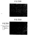
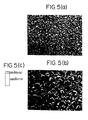
- Figs. 3 through 6 Each film consists of an indium and tin oxide layer of 800 angstrom in thickness and a tin oxide layer of 200 angstrom in thickness as particularly shown in Figs. 3(c), 4(c), 5(c) and 6(b).
- the microphotographs of Figs. 3(a) and 3(b) indicate a smooth transparent conductive film obtained according to a known procedure, revealing that the surface is very smooth.
- the magnifications in Figs. 3(a) and 3(b) are indicated as 50.4 KX and 99.8 KX which mean 50.4 x 10 3 and 99.8 x 10 3 magnifications, respectively. This is also applied to the other microphotographs.
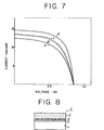
- the output characteristic of the known solar cell using the conductive film shown in Fig. 3 is indicated as curve a in Fig. 7.
- the solar cells of the invention using the conductive films shown in Figs. 4 through 6 have the output characteristic curves b, c and d, respectively. From the results of Fig. 7, it will be noted that rougher surfaces result in better output characteristic.
- the known solar cell as a is poorer than the solar cells of the present invention in all the characteristics. This is considered due to the fact that the rough or irregular surface of the conductive film contributes to reduce the reflection loss and increase the light absorption efficiency as compared with the smooth conductive film surface.
- the transparent conductive film having irregular or rough fine crystals or micro columns formed thereon may also be applied to a solar cell of the type which comprises a metal substrate such as SUS, a plurality of amorphous silicon layers superposed on the substrate, the transparent conductive film, and a metal electrode.
- a metal substrate such as SUS
- a plurality of amorphous silicon layers superposed on the substrate the transparent conductive film
- a metal electrode such as SUS
- an intermediate layer is established between the conductive film and the first silicon layer.
- the intermediate layer is made of indium oxide and/or tin oxide and the amorphous silicon.
- the refractive index of the intermediate layer 2' depends on the the mixing ratio of the oxide and the amorphous silicon and is intermediate between 2 and 4. An approximate value of the refractive index of the intermediate layer can be calculated according to the Maxwell-Garnet equation.
- the intermediate layer 2' if a filling rate of the micro columns or crystalline grains of the transparent conductive film 2 in the intermediate layer 2' increases, the refractive index of the intermediate layer 2' comes close to the refractive index of the conductive film 2. On the other hand, when the filling rate decreases, the refractive index of the intermediate layer 2' becomes close to the refractive index of the amorphous silicon layer. In order to reduce the refelectivity between the conductive film and the amorphous silicon layer, the intermediate layer 2' should preferably have a refractive index of about 3.0. In order to attain such a value, formation of crystalline grains is properly controlled by controlling the evaporation conditions, by which an optimum filling rate can be achieved.
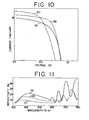
- three samples are fabricated by vacuum evaporating on a glass substrate indium oxide and then tin oxide under conditions of a feed of oxygen of10 cc/min. , an evaporation speed of 1 angstrom/sec.and a substrate temperature of 250°C (sample A), a feed of oxygen of 3 cc/min., an evaporation speed of 8 angstrom/sec.and a substrate temperature of 350°C (sample B), and a feed of oxygen of 1 cc/min. , an evaporation speed of 15 angstrom/sec.and a substrate temperature of 420°C (sample C).
- Figs. 9(a) through 9(c) These samples are subjected to electron microscopic observation with a magnification of 50 K X and microphotographs thereof are shown in Figs. 9(a) through 9(c).
- the sample A of Fig. 9(a) has a smooth surface and is a known conductive film.
- These samples are subsequently formed with a plurality of amorphous silicon layers and a metal electrode as usual.
- the output characteristic and reflectivity of these samples are measured with the results shown in Figs. 10 and 11, respectively.
- rougher surfaces of the conductive film result in a lower reflectivity over a wider range of wavelength and a higher output current or short-circuit current.
Landscapes
- Photovoltaic Devices (AREA)
Applications Claiming Priority (2)
| Application Number | Priority Date | Filing Date | Title |
|---|---|---|---|
| JP58176464A JPS6068663A (ja) | 1983-09-26 | 1983-09-26 | アモルフアスシリコン太陽電池 |
| JP176464/83 | 1983-09-26 |
Publications (3)
| Publication Number | Publication Date |
|---|---|
| EP0137291A2 true EP0137291A2 (de) | 1985-04-17 |
| EP0137291A3 EP0137291A3 (en) | 1986-07-30 |
| EP0137291B1 EP0137291B1 (de) | 1989-08-02 |
Family
ID=16014141
Family Applications (1)
| Application Number | Title | Priority Date | Filing Date |
|---|---|---|---|
| EP84110395A Expired EP0137291B1 (de) | 1983-09-26 | 1984-08-31 | Solarzellen aus amorphem Silizium |
Country Status (4)
| Country | Link |
|---|---|
| US (1) | US4746372A (de) |
| EP (1) | EP0137291B1 (de) |
| JP (1) | JPS6068663A (de) |
| DE (1) | DE3479272D1 (de) |
Cited By (4)
| Publication number | Priority date | Publication date | Assignee | Title |
|---|---|---|---|---|
| EP0213045B1 (de) * | 1985-08-20 | 1991-01-23 | Saint-Gobain Vitrage International | Verfahren zum Niederschlagen einer Siliziumdioxydbeschichtung mit einer unregelmässigen Oberfläche auf einem Glassubstrat |
| WO2000028603A1 (en) * | 1998-11-06 | 2000-05-18 | Pacific Solar Pty. Limited | TEXTURING OF GLASS BY SiO2 FILM |
| CN102254961A (zh) * | 2011-05-28 | 2011-11-23 | 惠州市易晖太阳能科技有限公司 | 一种太阳能电池专用绒面导电玻璃及其制备方法与应用 |
| EP2372777A3 (de) * | 2007-04-26 | 2012-05-30 | Guardian Industries Corp. | Frontelektrode mit transparenter leitender Beschichtung auf einem geätzten Glassubstrat für ein Photovoltaik-Element und Herstellungsverfahren dafür |
Families Citing this family (10)
| Publication number | Priority date | Publication date | Assignee | Title |
|---|---|---|---|---|
| US4808462A (en) * | 1987-05-22 | 1989-02-28 | Glasstech Solar, Inc. | Solar cell substrate |
| US5078803A (en) * | 1989-09-22 | 1992-01-07 | Siemens Solar Industries L.P. | Solar cells incorporating transparent electrodes comprising hazy zinc oxide |
| EP1929542A1 (de) * | 2005-08-30 | 2008-06-11 | Pilkington Group Limited | Lichtdurchlässigkeitsoptimierte beschichtete glasartikel für eine solarzelle und herstellungsverfahren |
| US8203073B2 (en) | 2006-11-02 | 2012-06-19 | Guardian Industries Corp. | Front electrode for use in photovoltaic device and method of making same |
| US8076571B2 (en) | 2006-11-02 | 2011-12-13 | Guardian Industries Corp. | Front electrode for use in photovoltaic device and method of making same |
| DE102007047088A1 (de) | 2007-10-01 | 2009-04-09 | Buskühl, Martin, Dr. | Fotovoltaik-Modul mit wenigstens einer Solarzelle |
| WO2009120330A2 (en) * | 2008-03-25 | 2009-10-01 | Corning Incorporated | Substrates for photovoltaics |
| DE112009001642B4 (de) * | 2008-07-07 | 2016-09-22 | Mitsubishi Electric Corp. | Dünnschichtsolarzelle und Verfahren zu deren Herstellung |
| US20110308585A1 (en) * | 2010-06-16 | 2011-12-22 | International Business Machines Corporation | Dual transparent conductive material layer for improved performance of photovoltaic devices |
| CN103872166A (zh) * | 2014-03-31 | 2014-06-18 | 惠州市易晖太阳能科技有限公司 | 一种铜铟镓硒薄膜太阳能电池的陷光结构及其制备方法 |
Family Cites Families (14)
| Publication number | Priority date | Publication date | Assignee | Title |
|---|---|---|---|---|
| IN152814B (de) * | 1978-08-08 | 1984-04-14 | Westinghouse Electric Corp | |
| US4281208A (en) * | 1979-02-09 | 1981-07-28 | Sanyo Electric Co., Ltd. | Photovoltaic device and method of manufacturing thereof |
| DE3048381C2 (de) * | 1980-12-22 | 1985-09-05 | Messerschmitt-Bölkow-Blohm GmbH, 8000 München | Dünnschicht-Solarzelle |
| JPS57157578A (en) * | 1981-03-23 | 1982-09-29 | Sumitomo Electric Ind Ltd | Active crystalline silicon thin film photovoltaic element |
| DE3280112D1 (de) * | 1981-07-17 | 1990-03-15 | Kanegafuchi Chemical Ind | Amorpher halbleiter und photovoltaische einrichtung aus amorphem silizium. |
| JPS5857756A (ja) * | 1981-10-01 | 1983-04-06 | Agency Of Ind Science & Technol | 非晶質太陽電池 |
| US4554727A (en) * | 1982-08-04 | 1985-11-26 | Exxon Research & Engineering Company | Method for making optically enhanced thin film photovoltaic device using lithography defined random surfaces |
| US4532537A (en) * | 1982-09-27 | 1985-07-30 | Rca Corporation | Photodetector with enhanced light absorption |
| US4599482A (en) * | 1983-03-07 | 1986-07-08 | Semiconductor Energy Lab. Co., Ltd. | Semiconductor photoelectric conversion device and method of making the same |
| JPS6034076A (ja) * | 1983-08-05 | 1985-02-21 | Taiyo Yuden Co Ltd | 非晶質シリコン太陽電池 |
| JPH0680837B2 (ja) * | 1983-08-29 | 1994-10-12 | 通商産業省工業技術院長 | 光路を延長した光電変換素子 |
| US4689438A (en) * | 1984-10-17 | 1987-08-25 | Sanyo Electric Co., Ltd. | Photovoltaic device |
| JPH0614554B2 (ja) * | 1985-03-22 | 1994-02-23 | 工業技術院長 | 薄膜太陽電池の製造方法 |
| US4683160A (en) * | 1985-05-09 | 1987-07-28 | Exxon Research And Engineering Company | Solar cells with correlated roughness substrate |
-
1983
- 1983-09-26 JP JP58176464A patent/JPS6068663A/ja active Pending
-
1984
- 1984-08-31 EP EP84110395A patent/EP0137291B1/de not_active Expired
- 1984-08-31 DE DE8484110395T patent/DE3479272D1/de not_active Expired
-
1986
- 1986-04-18 US US06/853,322 patent/US4746372A/en not_active Expired - Lifetime
Cited By (7)
| Publication number | Priority date | Publication date | Assignee | Title |
|---|---|---|---|---|
| EP0213045B1 (de) * | 1985-08-20 | 1991-01-23 | Saint-Gobain Vitrage International | Verfahren zum Niederschlagen einer Siliziumdioxydbeschichtung mit einer unregelmässigen Oberfläche auf einem Glassubstrat |
| WO2000028603A1 (en) * | 1998-11-06 | 2000-05-18 | Pacific Solar Pty. Limited | TEXTURING OF GLASS BY SiO2 FILM |
| WO2000028602A1 (en) * | 1998-11-06 | 2000-05-18 | Pacific Solar Pty Limited | Thin films with light trapping |
| US6420647B1 (en) | 1998-11-06 | 2002-07-16 | Pacific Solar Pty Limited | Texturing of glass by SiO2 film |
| US6538195B1 (en) | 1998-11-06 | 2003-03-25 | Pacific Solar Pty Limited | Thin films with light trapping |
| EP2372777A3 (de) * | 2007-04-26 | 2012-05-30 | Guardian Industries Corp. | Frontelektrode mit transparenter leitender Beschichtung auf einem geätzten Glassubstrat für ein Photovoltaik-Element und Herstellungsverfahren dafür |
| CN102254961A (zh) * | 2011-05-28 | 2011-11-23 | 惠州市易晖太阳能科技有限公司 | 一种太阳能电池专用绒面导电玻璃及其制备方法与应用 |
Also Published As
| Publication number | Publication date |
|---|---|
| US4746372A (en) | 1988-05-24 |
| EP0137291B1 (de) | 1989-08-02 |
| DE3479272D1 (en) | 1989-09-07 |
| JPS6068663A (ja) | 1985-04-19 |
| EP0137291A3 (en) | 1986-07-30 |
Similar Documents
| Publication | Publication Date | Title |
|---|---|---|
| EP0137291B1 (de) | Solarzellen aus amorphem Silizium | |
| EP0234222B1 (de) | Sonnenbatterie | |
| EP1100130B3 (de) | Silizium dünnschicht photoelektrische vorrichtung | |
| EP1142031B1 (de) | Dünnschichtsolarzelle auf Glas mit Siliziumdioxid-Texturierung und Herstellungsverfahren | |
| US4694116A (en) | Thin-film solar cell | |
| EP1189288B1 (de) | Photoelektrische umwandlungsanordnung | |
| US4592129A (en) | Method of making an integral, multiple layer antireflection coating by hydrogen ion implantation | |
| US4338482A (en) | Photovoltaic cell | |
| WO1999010933A1 (fr) | Transducteur photoelectrique a couche mince | |
| KR100295432B1 (ko) | 광전변환소자 | |
| JPS60208813A (ja) | 光電変換装置とその製造方法 | |
| JPH02245702A (ja) | 反射防止膜及びその製作方法 | |
| BRPI0616268A2 (pt) | substrato transparente, utilizaÇço do substrato, e, cÉlula solar | |
| JPS6233479A (ja) | 太陽電池 | |
| JPH07321362A (ja) | 光起電力装置 | |
| EP2351091B1 (de) | Photoelektrische Mehrfachsperrschichtanordnung und Prozess zu ihrer Herstellung | |
| US7718091B2 (en) | Coating which is applied to substrate, a solar cell, and method for applying the coating to the substrate | |
| US5064477A (en) | Radiant energy sensitive device and method | |
| JP3025392B2 (ja) | 薄膜太陽電池とその製造方法 | |
| JPS61120480A (ja) | 光電変換装置 | |
| JP2007266096A (ja) | 太陽電池及びその製造方法 | |
| JPS59125669A (ja) | 太陽電池 | |
| JPS6152992B2 (de) | ||
| JPH0575153A (ja) | 光電変換素子用透明導電膜及びその製造方法 | |
| Yates et al. | Optimization of solar cell performance using atmospheric pressure chemical vapour deposition deposited TCOs |
Legal Events
| Date | Code | Title | Description |
|---|---|---|---|
| PUAI | Public reference made under article 153(3) epc to a published international application that has entered the european phase |
Free format text: ORIGINAL CODE: 0009012 |
|
| 17P | Request for examination filed |
Effective date: 19840831 |
|
| AK | Designated contracting states |
Designated state(s): DE FR GB |
|
| PUAL | Search report despatched |
Free format text: ORIGINAL CODE: 0009013 |
|
| AK | Designated contracting states |
Kind code of ref document: A3 Designated state(s): DE FR GB |
|
| 17Q | First examination report despatched |
Effective date: 19880915 |
|
| GRAA | (expected) grant |
Free format text: ORIGINAL CODE: 0009210 |
|
| AK | Designated contracting states |
Kind code of ref document: B1 Designated state(s): DE FR GB |
|
| REF | Corresponds to: |
Ref document number: 3479272 Country of ref document: DE Date of ref document: 19890907 |
|
| ET | Fr: translation filed | ||
| PLBI | Opposition filed |
Free format text: ORIGINAL CODE: 0009260 |
|
| 26 | Opposition filed |
Opponent name: BSG TECHNISCHE BERATUNGS-GESELLSCHAFT MBH Effective date: 19900502 |
|
| PGFP | Annual fee paid to national office [announced via postgrant information from national office to epo] |
Ref country code: FR Payment date: 19930805 Year of fee payment: 10 |
|
| PGFP | Annual fee paid to national office [announced via postgrant information from national office to epo] |
Ref country code: GB Payment date: 19930823 Year of fee payment: 10 Ref country code: DE Payment date: 19930823 Year of fee payment: 10 |
|
| RDAG | Patent revoked |
Free format text: ORIGINAL CODE: 0009271 |
|
| STAA | Information on the status of an ep patent application or granted ep patent |
Free format text: STATUS: PATENT REVOKED |
|
| 27W | Patent revoked |
Effective date: 19940922 |
|
| GBPR | Gb: patent revoked under art. 102 of the ep convention designating the uk as contracting state |
Free format text: 940922 |