EP0137291A2 - Amorphous silicon solar cells - Google Patents
Amorphous silicon solar cells Download PDFInfo
- Publication number
- EP0137291A2 EP0137291A2 EP84110395A EP84110395A EP0137291A2 EP 0137291 A2 EP0137291 A2 EP 0137291A2 EP 84110395 A EP84110395 A EP 84110395A EP 84110395 A EP84110395 A EP 84110395A EP 0137291 A2 EP0137291 A2 EP 0137291A2
- Authority
- EP
- European Patent Office
- Prior art keywords
- amorphous silicon
- conductive film
- solar cell
- transparent conductive
- cell according
- Prior art date
- Legal status (The legal status is an assumption and is not a legal conclusion. Google has not performed a legal analysis and makes no representation as to the accuracy of the status listed.)
- Granted
Links
Images


Classifications
-
- H—ELECTRICITY
- H10—SEMICONDUCTOR DEVICES; ELECTRIC SOLID-STATE DEVICES NOT OTHERWISE PROVIDED FOR
- H10F—INORGANIC SEMICONDUCTOR DEVICES SENSITIVE TO INFRARED RADIATION, LIGHT, ELECTROMAGNETIC RADIATION OF SHORTER WAVELENGTH OR CORPUSCULAR RADIATION
- H10F10/00—Individual photovoltaic cells, e.g. solar cells
- H10F10/10—Individual photovoltaic cells, e.g. solar cells having potential barriers
- H10F10/17—Photovoltaic cells having only PIN junction potential barriers
-
- H—ELECTRICITY
- H10—SEMICONDUCTOR DEVICES; ELECTRIC SOLID-STATE DEVICES NOT OTHERWISE PROVIDED FOR
- H10F—INORGANIC SEMICONDUCTOR DEVICES SENSITIVE TO INFRARED RADIATION, LIGHT, ELECTROMAGNETIC RADIATION OF SHORTER WAVELENGTH OR CORPUSCULAR RADIATION
- H10F71/00—Manufacture or treatment of devices covered by this subclass
- H10F71/138—Manufacture of transparent electrodes, e.g. transparent conductive oxides [TCO] or indium tin oxide [ITO] electrodes
-
- Y—GENERAL TAGGING OF NEW TECHNOLOGICAL DEVELOPMENTS; GENERAL TAGGING OF CROSS-SECTIONAL TECHNOLOGIES SPANNING OVER SEVERAL SECTIONS OF THE IPC; TECHNICAL SUBJECTS COVERED BY FORMER USPC CROSS-REFERENCE ART COLLECTIONS [XRACs] AND DIGESTS
- Y02—TECHNOLOGIES OR APPLICATIONS FOR MITIGATION OR ADAPTATION AGAINST CLIMATE CHANGE
- Y02E—REDUCTION OF GREENHOUSE GAS [GHG] EMISSIONS, RELATED TO ENERGY GENERATION, TRANSMISSION OR DISTRIBUTION
- Y02E10/00—Energy generation through renewable energy sources
- Y02E10/50—Photovoltaic [PV] energy
- Y02E10/548—Amorphous silicon PV cells
Definitions
- This invention relates to the art of solar energy and more particularly, to amorphous silicon solar cells with improved light absorption efficiency and reflection- preventing or anti-reflective effect.
- ITO indium and tin oxide
- superposition of a plurality of amorphous silicon layers on the transparent electrode is generally carried out by a plasma CVD method or the like in which a gas such as monosilane (SiH 4 ) is decomposed under a low vacuum.
- a gas such as monosilane (SiH 4 ) is decomposed under a low vacuum.
- SiH 4 monosilane
- the severe decomposition conditions will cause indium and tin oxide to deteriorate.
- the iT0 electrode is currently coated on one surface thereof with Sn0 2 which is stable against plasma though lower in conductivity than ITO.
- the Sn0 2 -coated transparent electrode has been usually assessed with respect to electrical conductivity, stability against plasma and transparency, so that it has been generally accepted that the transparent electrode should preferably be as smooth as possible on the surfaces thereof. In this connection, however, according to our experiments where the surface condition of transparent electrode was changed, it was found that the absorption efficiency of light was better in rough surface than in smooth surface.
- a typical prior art solar cell comprising plural amorphous silicon layers has such a construction as particularly shown in Fig. 1.
- a solar cell S comprises a glass substrate 1, on which are superposed a transparent conductive film 2, a plurality of amorphous silicon layers, 3, 4, 5 and a metal electrode 6 in this order.
- the transparent conductive film 2 formed directly on the glass substrate has not only a function of withdrawing an output voltage of the cell to outside, but also a function as a anti-reflective film in order to reduce the reflectivity of incident light.
- the transparent conductive film made of indium oxide and tin oxide has a refractive index of about 2
- the amorphous silicon layers 3, 4, 5 have each a refractive index of about ⁇ 4.0. Because the tranparent conductive film 2 has such a refractive index value which almost satisfies the conditions of amplitude of non-reflection, proper choice of the film thickness will result in a small reflectivity at a certain wavelength as will be particularly seen from Fig. 2.
- the conductive film has the reflection- preventive effect at a certain wavelength, it exhibits a large reflectivity against incident light at different wavelengths, with the disadvantage that incident light covering a wide range of wavelengths cannot be effectively utilized.
- the reason why the transparent conductive film in the construction of known solar cells has the anti-reflective effect only at a certain wavelength is due to the fact that the transparent conductive film is formed of a single layer. If the conductive film is made of a multi-layered structure comprising layers having different refractive indices, a wider range of wavelengths will be covered for the anti-reflective effect.
- the present invention is characterized by a conductive transparent film which has micro columns or fine crystals formed at least one surface thereof. Because of the presence of micro columns on the surface of the film; light passed through a transparent glass substrate can be efficiently absorbed thereby improving the light absorption efficiency.
- the coarse grains on the surface are actually made of fine crystals or so-called micro columns of indium oxide and/or tin oxide.
- a first amorphous silicon layer is formed on the cosrse grain-bearing surface, the micro columns are filled in the silicon layer to form an intermediate layer where the micro columns and the amorphous silicon are admixed.
- This intermediate layer serves to prevent reflection of light passed through the transparent conductive film because the intermediate layer has a refractive index between the indices of the conductive layer and the amorphous silicon layer.
- the micro columns-bearing transparent conductive film may be applied to a solar cell of the type which makes use of a metal substrate, instead of the glass substrate, with similar results.
- An amorphous silicon solar cell S of the Pin type includes a glass substrate 1 and a transparent conductive film 2 formed on the substrate a by vacuum evaporation. On the film 2 are formed a plurality of silicon layers including, for example, a p-amorphous silicon layer 3, an i-amorphous silicon layer 4 and a n-amorphous silicon layer 5. Finally, a metal electrode 6 is formed on the n-amorphous silicon layer 5. Light is passed from the side of the glass substrate 1 as shown.
- the transparent conductive film 2 is formed on the glass substrate a by vacuum evaporation of indium oxide with or without further deposition of tin oxide.
- the transparent conductive film is finished to be as smooth as possible.
- the conductive film is preferred to be rough in view of light absorption efficiency.
- indium oxide and/or tin oxide is vacuum evaporated by any known techniques, such as an electron beam vacuum evaporation, under properly controlled conditions by which micro columns or fine crystals are developed on the surface of the conductive film 2.
- the feed of oxygen and the evaporation speed are controlled so that fine crystals or micro columns having a maximum height of 800 to 1200 angstrom are formed on the conductive film 2 which has usually a thickness of from 800 to 1200 angstrom.
- These evaporation conditions are very minute and should be experiementally confirmed.
- the vacuum evaporation conditions useful in the present invention are as follows: the feed of oxygen is 2 to 5 cc/min.; the evaporation speed is from 5 to 10 angstrom/sec. the temperature of substrate is from 300to400°C; and the evaporation time is from 1 to 4 minutes.
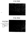
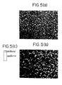
- Figs. 3 through 6 Each film consists of an indium and tin oxide layer of 800 angstrom in thickness and a tin oxide layer of 200 angstrom in thickness as particularly shown in Figs. 3(c), 4(c), 5(c) and 6(b).
- the microphotographs of Figs. 3(a) and 3(b) indicate a smooth transparent conductive film obtained according to a known procedure, revealing that the surface is very smooth.
- the magnifications in Figs. 3(a) and 3(b) are indicated as 50.4 KX and 99.8 KX which mean 50.4 x 10 3 and 99.8 x 10 3 magnifications, respectively. This is also applied to the other microphotographs.
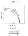
- the output characteristic of the known solar cell using the conductive film shown in Fig. 3 is indicated as curve a in Fig. 7.
- the solar cells of the invention using the conductive films shown in Figs. 4 through 6 have the output characteristic curves b, c and d, respectively. From the results of Fig. 7, it will be noted that rougher surfaces result in better output characteristic.
- the known solar cell as a is poorer than the solar cells of the present invention in all the characteristics. This is considered due to the fact that the rough or irregular surface of the conductive film contributes to reduce the reflection loss and increase the light absorption efficiency as compared with the smooth conductive film surface.
- the transparent conductive film having irregular or rough fine crystals or micro columns formed thereon may also be applied to a solar cell of the type which comprises a metal substrate such as SUS, a plurality of amorphous silicon layers superposed on the substrate, the transparent conductive film, and a metal electrode.
- a metal substrate such as SUS
- a plurality of amorphous silicon layers superposed on the substrate the transparent conductive film
- a metal electrode such as SUS
- an intermediate layer is established between the conductive film and the first silicon layer.
- the intermediate layer is made of indium oxide and/or tin oxide and the amorphous silicon.
- the refractive index of the intermediate layer 2' depends on the the mixing ratio of the oxide and the amorphous silicon and is intermediate between 2 and 4. An approximate value of the refractive index of the intermediate layer can be calculated according to the Maxwell-Garnet equation.
- the intermediate layer 2' if a filling rate of the micro columns or crystalline grains of the transparent conductive film 2 in the intermediate layer 2' increases, the refractive index of the intermediate layer 2' comes close to the refractive index of the conductive film 2. On the other hand, when the filling rate decreases, the refractive index of the intermediate layer 2' becomes close to the refractive index of the amorphous silicon layer. In order to reduce the refelectivity between the conductive film and the amorphous silicon layer, the intermediate layer 2' should preferably have a refractive index of about 3.0. In order to attain such a value, formation of crystalline grains is properly controlled by controlling the evaporation conditions, by which an optimum filling rate can be achieved.
- three samples are fabricated by vacuum evaporating on a glass substrate indium oxide and then tin oxide under conditions of a feed of oxygen of10 cc/min. , an evaporation speed of 1 angstrom/sec.and a substrate temperature of 250°C (sample A), a feed of oxygen of 3 cc/min., an evaporation speed of 8 angstrom/sec.and a substrate temperature of 350°C (sample B), and a feed of oxygen of 1 cc/min. , an evaporation speed of 15 angstrom/sec.and a substrate temperature of 420°C (sample C).
- Figs. 9(a) through 9(c) These samples are subjected to electron microscopic observation with a magnification of 50 K X and microphotographs thereof are shown in Figs. 9(a) through 9(c).
- the sample A of Fig. 9(a) has a smooth surface and is a known conductive film.
- These samples are subsequently formed with a plurality of amorphous silicon layers and a metal electrode as usual.
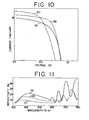
- the output characteristic and reflectivity of these samples are measured with the results shown in Figs. 10 and 11, respectively.
- rougher surfaces of the conductive film result in a lower reflectivity over a wider range of wavelength and a higher output current or short-circuit current.
Landscapes
- Photovoltaic Devices (AREA)
Abstract
Description
- This invention relates to the art of solar energy and more particularly, to amorphous silicon solar cells with improved light absorption efficiency and reflection- preventing or anti-reflective effect.
- For the fabrication of amorphous silicon solar cells, it is the usual practice to use indium and tin oxide (ITO) as a transparent electrode because of the excellent conductivity thereof. However, superposition of a plurality of amorphous silicon layers on the transparent electrode is generally carried out by a plasma CVD method or the like in which a gas such as monosilane (SiH4) is decomposed under a low vacuum. The severe decomposition conditions will cause indium and tin oxide to deteriorate. To avoid this, the iT0 electrode is currently coated on one surface thereof with Sn02 which is stable against plasma though lower in conductivity than ITO. The Sn02-coated transparent electrode has been usually assessed with respect to electrical conductivity, stability against plasma and transparency, so that it has been generally accepted that the transparent electrode should preferably be as smooth as possible on the surfaces thereof. In this connection, however, according to our experiments where the surface condition of transparent electrode was changed, it was found that the absorption efficiency of light was better in rough surface than in smooth surface.
- A typical prior art solar cell comprising plural amorphous silicon layers has such a construction as particularly shown in Fig. 1. A solar cell S comprises a glass substrate 1, on which are superposed a transparent conductive film 2, a plurality of amorphous silicon layers, 3, 4, 5 and a metal electrode 6 in this order. The transparent conductive film 2 formed directly on the glass substrate has not only a function of withdrawing an output voltage of the cell to outside, but also a function as a anti-reflective film in order to reduce the reflectivity of incident light.
- While the transparent conductive film made of indium oxide and tin oxide has a refractive index of about 2, the
amorphous silicon layers - However, while the conductive film has the reflection- preventive effect at a certain wavelength, it exhibits a large reflectivity against incident light at different wavelengths, with the disadvantage that incident light covering a wide range of wavelengths cannot be effectively utilized. The reason why the transparent conductive film in the construction of known solar cells has the anti-reflective effect only at a certain wavelength is due to the fact that the transparent conductive film is formed of a single layer. If the conductive film is made of a multi-layered structure comprising layers having different refractive indices, a wider range of wavelengths will be covered for the anti-reflective effect. This technique has already been carried out in camera lenses but application of the conductive film of the multi-layered structure needs a material having a refractive index, n, intermediate between those of the amorphous silicon layer and the transparent conductive film, i.e. 2<n<4. In addition, such a material should be conductive and optically transparent. Thus, choice of such material is practically difficult.
- It is an object of the invention to provide an amorphous silicon solar cell which comprises a transparent conductive film having coarse grains on the surfaces thereof whereby the light absorption efficiency of the conductive film is improved over the efficiency of a smooth transparent conductive film used in known solar cells.
- It is another object of the invention to provide an amorphous silicon solar cell which comprises an anti-reflective layer between a transparent conductive film and a plurality of amorphous silicon layers whereby reflectivity of incident light over a wide range of wavelengths can be suppressed to an extent.
- It is a further object of the invention to provide an amorphous silicon solar cell which is much improved in ' output current or short-circuit current.
- Broadly, the present invention is characterized by a conductive transparent film which has micro columns or fine crystals formed at least one surface thereof. Because of the presence of micro columns on the surface of the film; light passed through a transparent glass substrate can be efficiently absorbed thereby improving the light absorption efficiency. The coarse grains on the surface are actually made of fine crystals or so-called micro columns of indium oxide and/or tin oxide. When a first amorphous silicon layer is formed on the cosrse grain-bearing surface, the micro columns are filled in the silicon layer to form an intermediate layer where the micro columns and the amorphous silicon are admixed. This intermediate layer serves to prevent reflection of light passed through the transparent conductive film because the intermediate layer has a refractive index between the indices of the conductive layer and the amorphous silicon layer. The micro columns-bearing transparent conductive film may be applied to a solar cell of the type which makes use of a metal substrate, instead of the glass substrate, with similar results.
-
- Fig. 1 is a schematic sectional view of a typical construction of a conventional amorphous silicon solar cell;
- Fig. 2 is a graphical representation of the relation between reflectivity and wavelength for different thicknesses of transparent conductive film;
- Figs. 3(a) and 3(b) are microphotographs of a surface structure of a known transparent conductive film and Fig. 3(c) is a schematic view showing a thickness of the conductive film;
- Figs. 4(a) to 4(c) through 6(a) and 6(b) are similar to Figs. 3(a) to 3(c), respectively, in which Figs. 4(a), 4(b), 5(a), 5(b) and 6(a) show microphotographs of transparent conductive films of solar cells of the present invention and Figs. 4(c), 5(c) and 6(b) show thicknesses of the films;
- Fig. 7 is a graphical representation of output characteristics of solar cells using transparent conductive films indicated in Figs. 3 through 6, respectively;
- Fig. 8 is a schematic sectional view of a solar cell illustrating an intermediate layer formed between a transparent conductive film and an amorphous silicon layer according to the present invention;
- Figs. 9(a) through 9(c) are microphotographs of transparent conductive films formed under different treating conditions;
- Fig. 10 is a graphical representation of the relation between electric current and voltage of solar cells using the transparent conductive films shown in Figs. 9(a) through 9(c), respectively; and
- Fig. 11 is a graphical representation of the r-lation between reflectivity and wavelength for solar cells using the transparent conductive films of Figs. 9(a) through 9(c), respectively.
- The general construction of an amorphous silicon solar cell according to the invention is similar to known solar cells and is particularly illustrated with reference to Fig. 1. An amorphous silicon solar cell S of the Pin type includes a glass substrate 1 and a transparent conductive film 2 formed on the substrate a by vacuum evaporation. On the film 2 are formed a plurality of silicon layers including, for example, a p-
amorphous silicon layer 3, an i-amorphous silicon layer 4 and a n-amorphous silicon layer 5. Finally, a metal electrode 6 is formed on the n-amorphous silicon layer 5. Light is passed from the side of the glass substrate 1 as shown. - In the practice of the invention, the transparent conductive film 2 is formed on the glass substrate a by vacuum evaporation of indium oxide with or without further deposition of tin oxide. In the known practice, it generally accepted that the transparent conductive film is finished to be as smooth as possible. However, we have found that the conductive film is preferred to be rough in view of light absorption efficiency. In order to make the surface rough, indium oxide and/or tin oxide is vacuum evaporated by any known techniques, such as an electron beam vacuum evaporation, under properly controlled conditions by which micro columns or fine crystals are developed on the surface of the conductive film 2. More particularly, the feed of oxygen and the evaporation speed are controlled so that fine crystals or micro columns having a maximum height of 800 to 1200 angstrom are formed on the conductive film 2 which has usually a thickness of from 800 to 1200 angstrom. These evaporation conditions are very minute and should be experiementally confirmed. Usually, the vacuum evaporation conditions useful in the present invention are as follows: the feed of oxygen is 2 to 5 cc/min.; the evaporation speed is from 5 to 10 angstrom/sec. the temperature of substrate is from 300to400°C; and the evaporation time is from 1 to 4 minutes.
- Under different vacuum evaporation conditions, transparent conductive films having different micro columns are formed on glass substrates. The microphotographs of these films are shown in Figs. 3 through 6. Each film consists of an indium and tin oxide layer of 800 angstrom in thickness and a tin oxide layer of 200 angstrom in thickness as particularly shown in Figs. 3(c), 4(c), 5(c) and 6(b). The microphotographs of Figs. 3(a) and 3(b) indicate a smooth transparent conductive film obtained according to a known procedure, revealing that the surface is very smooth. In the photographs, the magnifications in Figs. 3(a) and 3(b) are indicated as 50.4 KX and 99.8 KX which mean 50.4 x 10 3 and 99.8 x 10³ magnifications, respectively. This is also applied to the other microphotographs.
- As will be seen from Figs. 4(a), 4(b), 5(a), 5(b) and 6(a) showing the microphotographs of the conductive films of the invention, cubic or column grains or crystals are formed on the film surface which is thus made rough.
- On the conductive films as shown in these figures are further formed a plurality of silicon layers and a metal electrode to obtain solar cells having such a construction as shown in Fig. 1.
- These cells are each subjected to measurement of an output characteristic. The output characteristic of the known solar cell using the conductive film shown in Fig. 3 is indicated as curve a in Fig. 7. The solar cells of the invention using the conductive films shown in Figs. 4 through 6 have the output characteristic curves b, c and d, respectively. From the results of Fig. 7, it will be noted that rougher surfaces result in better output characteristic.
- The characteristics of the solar cells including release voltage, Voc, short-circuit current, Isc, curve factor, FF, and conversion efficiency, h, are shown in Table below. In the table, sample Nos. a, b. c and d correspond to the solar cells using the conductive films indicated in Figs. 3 through 6, respectively.

- Thus, the known solar cell as a is poorer than the solar cells of the present invention in all the characteristics. This is considered due to the fact that the rough or irregular surface of the conductive film contributes to reduce the reflection loss and increase the light absorption efficiency as compared with the smooth conductive film surface.
- The transparent conductive film having irregular or rough fine crystals or micro columns formed thereon may also be applied to a solar cell of the type which comprises a metal substrate such as SUS, a plurality of amorphous silicon layers superposed on the substrate, the transparent conductive film, and a metal electrode. In this case, although the order of the superposed layers is different from the solar cell using glass substrate, similar results are obtained.
- Especially, when the plurality of amorphous silicon layers are formed on the micro column-bearing conductive film, an intermediate layer is established between the conductive film and the first silicon layer. This is particularly shown in Fig. 8 in which the plurality of amorphous silicon layers are generally indicated at 3' and the intermediate layer is indicated at 2'. The intermediate layer is made of indium oxide and/or tin oxide and the amorphous silicon. The refractive index of the intermediate layer 2' depends on the the mixing ratio of the oxide and the amorphous silicon and is intermediate between 2 and 4. An approximate value of the refractive index of the intermediate layer can be calculated according to the Maxwell-Garnet equation. According to the Maxwell-Garnet equation, if a filling rate of the micro columns or crystalline grains of the transparent conductive film 2 in the intermediate layer 2' increases, the refractive index of the intermediate layer 2' comes close to the refractive index of the conductive film 2. On the other hand, when the filling rate decreases, the refractive index of the intermediate layer 2' becomes close to the refractive index of the amorphous silicon layer. In order to reduce the refelectivity between the conductive film and the amorphous silicon layer, the intermediate layer 2' should preferably have a refractive index of about 3.0. In order to attain such a value, formation of crystalline grains is properly controlled by controlling the evaporation conditions, by which an optimum filling rate can be achieved.
- In order to confirm the effect of the intermediate layer, three samples are fabricated by vacuum evaporating on a glass substrate indium oxide and then tin oxide under conditions of a feed of oxygen of10 cc/min. , an evaporation speed of 1 angstrom/sec.and a substrate temperature of 250°C (sample A), a feed of oxygen of 3 cc/min., an evaporation speed of 8 angstrom/sec.and a substrate temperature of 350°C (sample B), and a feed of oxygen of 1 cc/min. , an evaporation speed of 15 angstrom/sec.and a substrate temperature of 420°C (sample C). These samples are subjected to electron microscopic observation with a magnification of 50 KX and microphotographs thereof are shown in Figs. 9(a) through 9(c). The sample A of Fig. 9(a) has a smooth surface and is a known conductive film. These samples are subsequently formed with a plurality of amorphous silicon layers and a metal electrode as usual. The output characteristic and reflectivity of these samples are measured with the results shown in Figs. 10 and 11, respectively. As will be clearly seen from Figs. 10 and 11, rougher surfaces of the conductive film result in a lower reflectivity over a wider range of wavelength and a higher output current or short-circuit current.
Claims (13)
Applications Claiming Priority (2)
| Application Number | Priority Date | Filing Date | Title |
|---|---|---|---|
| JP176464/83 | 1983-09-26 | ||
| JP58176464A JPS6068663A (en) | 1983-09-26 | 1983-09-26 | Amorphous silicon solar cell |
Publications (3)
| Publication Number | Publication Date |
|---|---|
| EP0137291A2 true EP0137291A2 (en) | 1985-04-17 |
| EP0137291A3 EP0137291A3 (en) | 1986-07-30 |
| EP0137291B1 EP0137291B1 (en) | 1989-08-02 |
Family
ID=16014141
Family Applications (1)
| Application Number | Title | Priority Date | Filing Date |
|---|---|---|---|
| EP84110395A Expired EP0137291B1 (en) | 1983-09-26 | 1984-08-31 | Amorphous silicon solar cells |
Country Status (4)
| Country | Link |
|---|---|
| US (1) | US4746372A (en) |
| EP (1) | EP0137291B1 (en) |
| JP (1) | JPS6068663A (en) |
| DE (1) | DE3479272D1 (en) |
Cited By (4)
| Publication number | Priority date | Publication date | Assignee | Title |
|---|---|---|---|---|
| EP0213045B1 (en) * | 1985-08-20 | 1991-01-23 | Saint-Gobain Vitrage International | Process for depositing a silica coating with an irregular surface on a glass substrate |
| WO2000028603A1 (en) * | 1998-11-06 | 2000-05-18 | Pacific Solar Pty. Limited | TEXTURING OF GLASS BY SiO2 FILM |
| CN102254961A (en) * | 2011-05-28 | 2011-11-23 | 惠州市易晖太阳能科技有限公司 | Conductive suede glass special for solar cells, and preparation method and application thereof |
| EP2372777A3 (en) * | 2007-04-26 | 2012-05-30 | Guardian Industries Corp. | Front electrode including transparent conductive coating on patterned glass substrate for use in photovoltaic device and method of making same |
Families Citing this family (10)
| Publication number | Priority date | Publication date | Assignee | Title |
|---|---|---|---|---|
| US4808462A (en) * | 1987-05-22 | 1989-02-28 | Glasstech Solar, Inc. | Solar cell substrate |
| US5078803A (en) * | 1989-09-22 | 1992-01-07 | Siemens Solar Industries L.P. | Solar cells incorporating transparent electrodes comprising hazy zinc oxide |
| MY160173A (en) | 2005-08-30 | 2017-02-28 | Pilkington Group Ltd | Light transmittance optimizing coated glass article for solar cell and method for making |
| US8203073B2 (en) | 2006-11-02 | 2012-06-19 | Guardian Industries Corp. | Front electrode for use in photovoltaic device and method of making same |
| US8076571B2 (en) | 2006-11-02 | 2011-12-13 | Guardian Industries Corp. | Front electrode for use in photovoltaic device and method of making same |
| DE102007047088A1 (en) | 2007-10-01 | 2009-04-09 | Buskühl, Martin, Dr. | Photovoltaic module with at least one solar cell |
| WO2009120330A2 (en) * | 2008-03-25 | 2009-10-01 | Corning Incorporated | Substrates for photovoltaics |
| JP5127925B2 (en) * | 2008-07-07 | 2013-01-23 | 三菱電機株式会社 | Thin film solar cell and manufacturing method thereof |
| US20110308585A1 (en) * | 2010-06-16 | 2011-12-22 | International Business Machines Corporation | Dual transparent conductive material layer for improved performance of photovoltaic devices |
| CN103872166A (en) * | 2014-03-31 | 2014-06-18 | 惠州市易晖太阳能科技有限公司 | Light trapping structure of copper indium gallium selenium thin film solar cell and preparation method thereof |
Family Cites Families (14)
| Publication number | Priority date | Publication date | Assignee | Title |
|---|---|---|---|---|
| IN152814B (en) * | 1978-08-08 | 1984-04-14 | Westinghouse Electric Corp | |
| US4281208A (en) * | 1979-02-09 | 1981-07-28 | Sanyo Electric Co., Ltd. | Photovoltaic device and method of manufacturing thereof |
| DE3048381C2 (en) * | 1980-12-22 | 1985-09-05 | Messerschmitt-Bölkow-Blohm GmbH, 8000 München | Thin film solar cell |
| JPS57157578A (en) * | 1981-03-23 | 1982-09-29 | Sumitomo Electric Ind Ltd | Active crystalline silicon thin film photovoltaic element |
| DE3280112D1 (en) * | 1981-07-17 | 1990-03-15 | Kanegafuchi Chemical Ind | AMORPHOUS SEMICONDUCTOR AND PHOTOVOLTAIC DEVICE MADE OF AMORPHIC SILICON. |
| JPS5857756A (en) * | 1981-10-01 | 1983-04-06 | Agency Of Ind Science & Technol | Amorphous silicon solar battery |
| US4554727A (en) * | 1982-08-04 | 1985-11-26 | Exxon Research & Engineering Company | Method for making optically enhanced thin film photovoltaic device using lithography defined random surfaces |
| US4532537A (en) * | 1982-09-27 | 1985-07-30 | Rca Corporation | Photodetector with enhanced light absorption |
| US4599482A (en) * | 1983-03-07 | 1986-07-08 | Semiconductor Energy Lab. Co., Ltd. | Semiconductor photoelectric conversion device and method of making the same |
| JPS6034076A (en) * | 1983-08-05 | 1985-02-21 | Taiyo Yuden Co Ltd | Amorphous silicon solar cell |
| JPH0680837B2 (en) * | 1983-08-29 | 1994-10-12 | 通商産業省工業技術院長 | Photoelectric conversion element with extended optical path |
| US4689438A (en) * | 1984-10-17 | 1987-08-25 | Sanyo Electric Co., Ltd. | Photovoltaic device |
| JPH0614554B2 (en) * | 1985-03-22 | 1994-02-23 | 工業技術院長 | Method of manufacturing thin film solar cell |
| US4683160A (en) * | 1985-05-09 | 1987-07-28 | Exxon Research And Engineering Company | Solar cells with correlated roughness substrate |
-
1983
- 1983-09-26 JP JP58176464A patent/JPS6068663A/en active Pending
-
1984
- 1984-08-31 EP EP84110395A patent/EP0137291B1/en not_active Expired
- 1984-08-31 DE DE8484110395T patent/DE3479272D1/en not_active Expired
-
1986
- 1986-04-18 US US06/853,322 patent/US4746372A/en not_active Expired - Lifetime
Cited By (7)
| Publication number | Priority date | Publication date | Assignee | Title |
|---|---|---|---|---|
| EP0213045B1 (en) * | 1985-08-20 | 1991-01-23 | Saint-Gobain Vitrage International | Process for depositing a silica coating with an irregular surface on a glass substrate |
| WO2000028603A1 (en) * | 1998-11-06 | 2000-05-18 | Pacific Solar Pty. Limited | TEXTURING OF GLASS BY SiO2 FILM |
| WO2000028602A1 (en) * | 1998-11-06 | 2000-05-18 | Pacific Solar Pty Limited | Thin films with light trapping |
| US6420647B1 (en) | 1998-11-06 | 2002-07-16 | Pacific Solar Pty Limited | Texturing of glass by SiO2 film |
| US6538195B1 (en) | 1998-11-06 | 2003-03-25 | Pacific Solar Pty Limited | Thin films with light trapping |
| EP2372777A3 (en) * | 2007-04-26 | 2012-05-30 | Guardian Industries Corp. | Front electrode including transparent conductive coating on patterned glass substrate for use in photovoltaic device and method of making same |
| CN102254961A (en) * | 2011-05-28 | 2011-11-23 | 惠州市易晖太阳能科技有限公司 | Conductive suede glass special for solar cells, and preparation method and application thereof |
Also Published As
| Publication number | Publication date |
|---|---|
| US4746372A (en) | 1988-05-24 |
| EP0137291A3 (en) | 1986-07-30 |
| JPS6068663A (en) | 1985-04-19 |
| EP0137291B1 (en) | 1989-08-02 |
| DE3479272D1 (en) | 1989-09-07 |
Similar Documents
| Publication | Publication Date | Title |
|---|---|---|
| EP0137291B1 (en) | Amorphous silicon solar cells | |
| EP0234222B1 (en) | Solar battery | |
| EP1100130B1 (en) | Silicon-base thin-film photoelectric device | |
| EP1142031B1 (en) | Thin film silicon solar cell on glass having a texturing silicon dioxide layer and manufacturing method | |
| US4694116A (en) | Thin-film solar cell | |
| EP1189288B1 (en) | Photoelectric conversion device | |
| US4592129A (en) | Method of making an integral, multiple layer antireflection coating by hydrogen ion implantation | |
| US4338482A (en) | Photovoltaic cell | |
| WO1999010933A1 (en) | Thin film photoelectric transducer | |
| KR100295432B1 (en) | Photoelectric conversion element | |
| JPS60208813A (en) | Photoelectric converting device and manufacture therefor | |
| JPH02245702A (en) | Anti-reflection film and its manufacturing method | |
| BRPI0616268A2 (en) | transparent substrate, substrate utilization, and solar cell | |
| JPS6233479A (en) | solar cells | |
| JPH07321362A (en) | Photovoltaic device | |
| EP2351091B1 (en) | Multiple-junction photoelectric device and its production process | |
| US7718091B2 (en) | Coating which is applied to substrate, a solar cell, and method for applying the coating to the substrate | |
| US5064477A (en) | Radiant energy sensitive device and method | |
| JP3025392B2 (en) | Thin film solar cell and manufacturing method | |
| JPS61120480A (en) | Photoelectric converter | |
| JP2007266096A (en) | Solar cell and its manufacturing method | |
| JPS59125669A (en) | Solar battery | |
| JPS6152992B2 (en) | ||
| JPH0575153A (en) | Transparent conductive film for photoelectric conversion element and its production | |
| Yates et al. | Optimization of solar cell performance using atmospheric pressure chemical vapour deposition deposited TCOs |
Legal Events
| Date | Code | Title | Description |
|---|---|---|---|
| PUAI | Public reference made under article 153(3) epc to a published international application that has entered the european phase |
Free format text: ORIGINAL CODE: 0009012 |
|
| 17P | Request for examination filed |
Effective date: 19840831 |
|
| AK | Designated contracting states |
Designated state(s): DE FR GB |
|
| PUAL | Search report despatched |
Free format text: ORIGINAL CODE: 0009013 |
|
| AK | Designated contracting states |
Kind code of ref document: A3 Designated state(s): DE FR GB |
|
| 17Q | First examination report despatched |
Effective date: 19880915 |
|
| GRAA | (expected) grant |
Free format text: ORIGINAL CODE: 0009210 |
|
| AK | Designated contracting states |
Kind code of ref document: B1 Designated state(s): DE FR GB |
|
| REF | Corresponds to: |
Ref document number: 3479272 Country of ref document: DE Date of ref document: 19890907 |
|
| ET | Fr: translation filed | ||
| PLBI | Opposition filed |
Free format text: ORIGINAL CODE: 0009260 |
|
| 26 | Opposition filed |
Opponent name: BSG TECHNISCHE BERATUNGS-GESELLSCHAFT MBH Effective date: 19900502 |
|
| PGFP | Annual fee paid to national office [announced via postgrant information from national office to epo] |
Ref country code: FR Payment date: 19930805 Year of fee payment: 10 |
|
| PGFP | Annual fee paid to national office [announced via postgrant information from national office to epo] |
Ref country code: GB Payment date: 19930823 Year of fee payment: 10 Ref country code: DE Payment date: 19930823 Year of fee payment: 10 |
|
| RDAG | Patent revoked |
Free format text: ORIGINAL CODE: 0009271 |
|
| STAA | Information on the status of an ep patent application or granted ep patent |
Free format text: STATUS: PATENT REVOKED |
|
| 27W | Patent revoked |
Effective date: 19940922 |
|
| GBPR | Gb: patent revoked under art. 102 of the ep convention designating the uk as contracting state |
Free format text: 940922 |