EP0136022A2 - Dynamischer Randomspeicher - Google Patents
Dynamischer Randomspeicher Download PDFInfo
- Publication number
- EP0136022A2 EP0136022A2 EP84305446A EP84305446A EP0136022A2 EP 0136022 A2 EP0136022 A2 EP 0136022A2 EP 84305446 A EP84305446 A EP 84305446A EP 84305446 A EP84305446 A EP 84305446A EP 0136022 A2 EP0136022 A2 EP 0136022A2
- Authority
- EP
- European Patent Office
- Prior art keywords
- transistor
- amplifier
- node
- output
- signal
- Prior art date
- Legal status (The legal status is an assumption and is not a legal conclusion. Google has not performed a legal analysis and makes no representation as to the accuracy of the status listed.)
- Granted
Links
Images


Classifications
-
- G—PHYSICS
- G11—INFORMATION STORAGE
- G11C—STATIC STORES
- G11C7/00—Arrangements for writing information into, or reading information out from, a digital store
- G11C7/10—Input/output [I/O] data interface arrangements, e.g. I/O data control circuits, I/O data buffers
- G11C7/1051—Data output circuits, e.g. read-out amplifiers, data output buffers, data output registers, data output level conversion circuits
- G11C7/106—Data output latches
-
- G—PHYSICS
- G11—INFORMATION STORAGE
- G11C—STATIC STORES
- G11C11/00—Digital stores characterised by the use of particular electric or magnetic storage elements; Storage elements therefor
- G11C11/21—Digital stores characterised by the use of particular electric or magnetic storage elements; Storage elements therefor using electric elements
- G11C11/34—Digital stores characterised by the use of particular electric or magnetic storage elements; Storage elements therefor using electric elements using semiconductor devices
- G11C11/40—Digital stores characterised by the use of particular electric or magnetic storage elements; Storage elements therefor using electric elements using semiconductor devices using transistors
- G11C11/401—Digital stores characterised by the use of particular electric or magnetic storage elements; Storage elements therefor using electric elements using semiconductor devices using transistors forming cells needing refreshing or charge regeneration, i.e. dynamic cells
- G11C11/4063—Auxiliary circuits, e.g. for addressing, decoding, driving, writing, sensing or timing
- G11C11/407—Auxiliary circuits, e.g. for addressing, decoding, driving, writing, sensing or timing for memory cells of the field-effect type
- G11C11/409—Read-write [R-W] circuits
- G11C11/4091—Sense or sense/refresh amplifiers, or associated sense circuitry, e.g. for coupled bit-line precharging, equalising or isolating
-
- G—PHYSICS
- G11—INFORMATION STORAGE
- G11C—STATIC STORES
- G11C7/00—Arrangements for writing information into, or reading information out from, a digital store
- G11C7/06—Sense amplifiers; Associated circuits, e.g. timing or triggering circuits
- G11C7/062—Differential amplifiers of non-latching type, e.g. comparators, long-tailed pairs
-
- G—PHYSICS
- G11—INFORMATION STORAGE
- G11C—STATIC STORES
- G11C7/00—Arrangements for writing information into, or reading information out from, a digital store
- G11C7/10—Input/output [I/O] data interface arrangements, e.g. I/O data control circuits, I/O data buffers
- G11C7/1051—Data output circuits, e.g. read-out amplifiers, data output buffers, data output registers, data output level conversion circuits
- G11C7/1069—I/O lines read out arrangements
Definitions
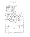
- the present invention relates to a dynamic random access memory (hereinafter referred to as a "d - RAM”), and more particularly to that which is capable of maintaining the level of output data during the hidden-refresh operation.
- a dynamic random access memory hereinafter referred to as a "d - RAM”
- the reference numeral 11 designates a pre-amplifier intended to amplify data which is read out from a memory cell accessed by an address signal from the outside. The detailed construction thereof is shown in Figure 2.
- the reference numeral 12 designates a main-amplifier intended to amplify the output of the pre-amplifier 11, and output the amplified signal as an output data Do. The detailed construction thereof is shown in Figure 3.
- the reference numeral 13 designates a driver circuit intended to output a driving signal for driving the main-amplifier 12 to the node N3.
- the driver circuit 13 which is constituted by internal transistors Ql, Q2, Q3 and internal nodes Nl, N2, the drain of the transistor Ql is connected to the power supply (Vcc) terminal, and the source thereof is connected to the third node N3 at which the driving signal is obtained.
- the drain of the transistor Q2 is connected to the third node N3, the source thereof is connected to the earth (Vss), and the gate thereof is connected to the drain of the transistor Q3.
- the drain of the transistor Q3 is connected to the first node Nl, the source thereof is connected to the earth (Vss), and the gate thereof is connected to the second node N2.
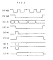
- Figure 4 which shows a timing diagram in a so-called hidden-refresh mode
- the (a) shows an inverted signal of Row Address Strobe signal (hereinafter referred to as RAS)
- the (b) shows an inverted signal of Column Address Strobe signal (hereinafter referred to as "CAS")
- the (c) shows an address signal Ai from the outside
- the (d) shows a signal at the internal node Nl
- the (e) shows a signal at the internal node N2
- the (f) shows a driving signal at the internal node N3
- the (g) and (h) show the outputs D and from the pre-amplifier 11, respectively
- the (i) shows the output data Do.
- the hidden-refresh is operated in such a manner that when the RAS signal falls down on a condition that the CAS signal is low, refreshs of all the memory cells which have the row address designated by the row address signal are executed and completed at the timing when the RAS signal rises up.
- the timing when the CAS signal falls down while the RAS signal is low data of the memory cell which has the row and column address designated by the address signal at that timing is output from the memory as the output data Do.
- the "hidden-refresh" means that the refreshs of memory cells are excecuted while data is output from the memory normally.
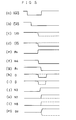
- the (a) shows the RAS signal
- the (b) shows the CAS signal
- the (c) and (d) show the signals of the I/O bus line 23 and I/O bus line 24 respectively
- the (e) shows a set signal Os input to the pre-amplifier 11
- the (f) shows a signal at the node N4
- the (g) shows a signal ⁇ c input to the pre-amplifier 11
- the (h) and (i) shows the outputs D and 0 from the pre-amplifier 11 respectively
- the (j) shows the driving output at the node N3
- the (k) and (1) show signals at the node N7 and N8 respectively
- the (m) shows the data output Do of the driving circuit 13.
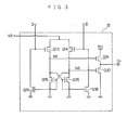
- the information stored in the memory cell selected among the memory cells of the memory cell array 21 is transmitted to the I/O bus line 23 and I/O bus line 24 as complimentary signals (refer to Figure 5 (c), (d)) through the I/O control circuit 22.
- the I/O bus line 23 and the I/O bus line 24 are connected to the drains of the transistors Q5 and Q6 respectively, both of which constitute a flip-flop in the pre-amplifier 11.
- the flip-flop is activated by the rising of a set signal Os (refer to Figure 5 (e)) input to the pre-amplifier 11 which signal turns on the transistor Q21, thereby making the node N4 discharge.
- the nodes N5 and N6 are pre-charged to a high voltage through the transistors Q7 and Q8 by the pre-charge signal ⁇ p, respectively.
- the I/O bus line 23 is at "H” (high level)
- the I/O bus line 24 is at "L” (low level)
- these signals are amplified by the flip-flop, then the transistor Q9 is turned off, the transistor Q10 is turned on, and the node N6 is discharged to the earth through the transistors Q10 and Q21.
- the transistor Qll which connects between the node N5 and the output D, and the transistor Q12 which connects between the node N6 and the output are both cut-off transistors which enhances the boot-strap effect of the main-amplifier 12.
- the voltage at the driving output node N3 rises at the timing when the outputs D, D of the pre-amplifier 11 are transmitted to the gates of the transistors Q13, Q14, whereby the voltages of the nodes N7, N8 are determined in accordance with the outputs D, D ⁇ of the pre-amplifier 11 (refer to Figure 5 (k), (1)).
- the voltages of the nodes N7, N8 are amplified by the transistors Q15, Q16 in flip-flop connection.
- the transistors Q17 and Q18 are arranged so as to discharge completely the gate voltage of either of the transistors Q13 and Q14 which is in OFF state. Either of the output transistors Q19, Q20 is turned on in accordance with the voltage of the nodes N7, N8, thereby determining the level of data output Do (refer to Figure 5 (m)).
- the mode shown in Figure 4 is that where the CAS signal is made "L" in the first cycle, the column addresses are taken out to execute a read-out cycle, thereby maintaining the output data Do as it is, and thereafter the RAS-only-refresh is continued with the CAS signal being held at "L” in the usual RAS-only-refresh mode. Meanwhile, the output data Do from the main-amplifier 12 is held.
- the voltage of the node N2 which is connected to the gate of the transistor Q3 which is arranged so as to place the node N1 to the earth which node (Nl) is connected to the gate of the transistor Q2, will become “L” at the rising of the RAS signal shown in Figure 4 (a), as apparent from Figure 4 (e), with keeping the state "L” during the hidden-refresh mode. Accordingly, the "L” level of the node N1 (refer to Figure 4 (d)) is an unstable one which is not connected to the earth (Vss) during the hidden-refresh.
- the voltage of the node N1 varies to the plus side caused by the coupling of noise voltages which arises accompanied with the circuit operation of the RAS system circuit, thereby decreasing the voltage of the driving output N3.
- the outputs D and 0 of the pre-amplifier 11 (refer to Figure 4 (g), (h)) are reset by the rising of the RAS signal (refer to Figure 4 (a)).
- the present invention is directed to solve the problems pointed out above, and has for its object to provide a dynamic random access memory capable of holding the level of output data in the hidden-refresh operation.
- a d-RAM wherein a transistor, to the gate whereof the driving output is supplied, is connected between the gate of the driving transistor of the driver circuit and the earth, whereby a latch circuit is constituted between the node of the driving output and the gate of the driving transistor.
- the reference character Q4 designates a transistor to the gate whereof the driving output at the node N3 is supplied, with the drain thereof being connected to the node Nl, and with the source thereof being connected to the earth (Vss).
- the drain of the transistor Ql is connected to the power supply (Vcc) terminal and the source thereof is connected to the third node N3 whereat the driving output is obtained.
- the drain of the transistor (first transistor) Q2 is connected to the third node N3, the source thereof is connected to the earth (Vss), and the gate thereof is connected to the drain of the transistor (second transistor) Q4.
- the drain of the transistor Q3 is connected to the node Nl, the source thereof is connected to the earth (Vss), and the gate thereof is connected to the second node N2.
- the transistor Q4 is held at its ON state while the driving output N3 is held "H” after the outputs D, D of the pre-amplifier 11 are reset, whereby the node N1 is connected to the earth (Vss), and the voltage of the node N1 does not arise, regardless of the couplings of noises accompanied with the operation of the RAS system circuit.
- the transistor Q2 is held at its OFF state during the hidden-refresh operation, whereby the driving output N3 is held at "H” and the output data Do from the main-amplifier 12 is maintained at its level. This is caused by the function of the latch circuit constituted by the nodes Nl, N2 and transistors Q4, Q2.
- a latch is constituted between the node whereat the driving output is obtained and the gate of the driving transistor, thereby realizing a d-RAM wherein the level of output data does not decrease in the hidden-refresh operation.
Landscapes
- Engineering & Computer Science (AREA)
- Microelectronics & Electronic Packaging (AREA)
- Computer Hardware Design (AREA)
- Dram (AREA)
Applications Claiming Priority (2)
| Application Number | Priority Date | Filing Date | Title |
|---|---|---|---|
| JP58156701A JPS6050694A (ja) | 1983-08-26 | 1983-08-26 | ダイナミツク・ランダム・アクセス・メモリ |
| JP156701/83 | 1983-08-26 |
Publications (3)
| Publication Number | Publication Date |
|---|---|
| EP0136022A2 true EP0136022A2 (de) | 1985-04-03 |
| EP0136022A3 EP0136022A3 (en) | 1986-12-10 |
| EP0136022B1 EP0136022B1 (de) | 1990-07-25 |
Family
ID=15633443
Family Applications (1)
| Application Number | Title | Priority Date | Filing Date |
|---|---|---|---|
| EP84305446A Expired - Lifetime EP0136022B1 (de) | 1983-08-26 | 1984-08-09 | Dynamischer Randomspeicher |
Country Status (4)
| Country | Link |
|---|---|
| US (1) | US4641281A (de) |
| EP (1) | EP0136022B1 (de) |
| JP (1) | JPS6050694A (de) |
| DE (1) | DE3482806D1 (de) |
Cited By (1)
| Publication number | Priority date | Publication date | Assignee | Title |
|---|---|---|---|---|
| GB2326496A (en) * | 1997-06-20 | 1998-12-23 | Hyundai Electronics Ind | A semiconductor device having a electric charge amplifier for amplifying bit line electric charge |
Families Citing this family (2)
| Publication number | Priority date | Publication date | Assignee | Title |
|---|---|---|---|---|
| JPS60248560A (ja) * | 1984-05-22 | 1985-12-09 | Fuji Photo Film Co Ltd | 集積束受渡し方法 |
| US5745914A (en) * | 1996-02-09 | 1998-04-28 | International Business Machines Corporation | Technique for converting system signals from one address configuration to a different address configuration |
Family Cites Families (4)
| Publication number | Priority date | Publication date | Assignee | Title |
|---|---|---|---|---|
| US4039861A (en) * | 1976-02-09 | 1977-08-02 | International Business Machines Corporation | Cross-coupled charge transfer sense amplifier circuits |
| JPS5922316B2 (ja) * | 1976-02-24 | 1984-05-25 | 株式会社東芝 | ダイナミツクメモリ装置 |
| JPS56130885A (en) * | 1980-03-18 | 1981-10-14 | Fujitsu Ltd | Address buffer circuit |
| JPS5782281A (en) * | 1980-11-07 | 1982-05-22 | Hitachi Ltd | Output level storage circuit |
-
1983
- 1983-08-26 JP JP58156701A patent/JPS6050694A/ja active Pending
-
1984
- 1984-08-08 US US06/638,675 patent/US4641281A/en not_active Expired - Lifetime
- 1984-08-09 DE DE8484305446T patent/DE3482806D1/de not_active Expired - Lifetime
- 1984-08-09 EP EP84305446A patent/EP0136022B1/de not_active Expired - Lifetime
Cited By (3)
| Publication number | Priority date | Publication date | Assignee | Title |
|---|---|---|---|---|
| GB2326496A (en) * | 1997-06-20 | 1998-12-23 | Hyundai Electronics Ind | A semiconductor device having a electric charge amplifier for amplifying bit line electric charge |
| US6226207B1 (en) | 1997-06-20 | 2001-05-01 | Hyundai Electronics Industries Co., Ltd. | Semiconductor device having an electric charge amplifier for amplifying bit line electric charge |
| GB2326496B (en) * | 1997-06-20 | 2002-02-20 | Hyundai Electronics Ind | A semiconductor device having a electric charge amplifier for amplifying bit line electric charge |
Also Published As
| Publication number | Publication date |
|---|---|
| EP0136022A3 (en) | 1986-12-10 |
| US4641281A (en) | 1987-02-03 |
| JPS6050694A (ja) | 1985-03-20 |
| EP0136022B1 (de) | 1990-07-25 |
| DE3482806D1 (de) | 1990-08-30 |
Similar Documents
| Publication | Publication Date | Title |
|---|---|---|
| JP2663838B2 (ja) | 半導体集積回路装置 | |
| US5007024A (en) | Semiconductor memory device with sense amplifier controller | |
| JP3101298B2 (ja) | 半導体メモリ装置 | |
| JPH0713857B2 (ja) | 半導体記憶装置 | |
| US4837465A (en) | Single rail CMOS register array and sense amplifier circuit therefor | |
| JPH0241109B2 (de) | ||
| US5323345A (en) | Semiconductor memory device having read/write circuitry | |
| KR100297717B1 (ko) | 반도체메모리의입출력선프리차아지회로및이를사용하는반도체메모리 | |
| US4722074A (en) | Semiconductor storage unit with I/O bus precharging and equalization | |
| JPH05282868A (ja) | 半導体記憶装置 | |
| JPS633394B2 (de) | ||
| US5014246A (en) | Semiconductor memory device having shared sense amplifier and operating method thereof | |
| JPS6288197A (ja) | ダイナミツクランダムアクセスメモリ装置 | |
| US4238841A (en) | Dynamic semiconductor memory read/write access circuit | |
| US4734889A (en) | Semiconductor memory | |
| US4992983A (en) | Semiconductor memory device with an improved write control circuit | |
| US4380055A (en) | Static RAM memory cell | |
| JPH0636556A (ja) | ダイナミックram | |
| US4641281A (en) | Dynamic random access memory with hidden refresh control | |
| US4792924A (en) | Single rail CMOS register array and sense amplifier circuit therefor | |
| US4583202A (en) | Semiconductor memory device | |
| JP2786420B2 (ja) | データリード/ライト方法及びその装置 | |
| US5469392A (en) | Semiconductor memory | |
| JP2523736B2 (ja) | 半導体記憶装置 | |
| JP2792258B2 (ja) | ダイナミックramの読み出し回路 |
Legal Events
| Date | Code | Title | Description |
|---|---|---|---|
| PUAI | Public reference made under article 153(3) epc to a published international application that has entered the european phase |
Free format text: ORIGINAL CODE: 0009012 |
|
| AK | Designated contracting states |
Designated state(s): DE FR GB |
|
| PUAL | Search report despatched |
Free format text: ORIGINAL CODE: 0009013 |
|
| AK | Designated contracting states |
Kind code of ref document: A3 Designated state(s): DE FR GB |
|
| 17P | Request for examination filed |
Effective date: 19870223 |
|
| 17Q | First examination report despatched |
Effective date: 19880324 |
|
| GRAA | (expected) grant |
Free format text: ORIGINAL CODE: 0009210 |
|
| AK | Designated contracting states |
Kind code of ref document: B1 Designated state(s): DE FR GB |
|
| REF | Corresponds to: |
Ref document number: 3482806 Country of ref document: DE Date of ref document: 19900830 |
|
| ET | Fr: translation filed | ||
| PLBE | No opposition filed within time limit |
Free format text: ORIGINAL CODE: 0009261 |
|
| STAA | Information on the status of an ep patent application or granted ep patent |
Free format text: STATUS: NO OPPOSITION FILED WITHIN TIME LIMIT |
|
| 26N | No opposition filed | ||
| REG | Reference to a national code |
Ref country code: GB Ref legal event code: 746 Effective date: 19950809 |
|
| REG | Reference to a national code |
Ref country code: FR Ref legal event code: D6 |
|
| REG | Reference to a national code |
Ref country code: GB Ref legal event code: IF02 |
|
| PGFP | Annual fee paid to national office [announced via postgrant information from national office to epo] |
Ref country code: GB Payment date: 20030806 Year of fee payment: 20 |
|
| PGFP | Annual fee paid to national office [announced via postgrant information from national office to epo] |
Ref country code: FR Payment date: 20030808 Year of fee payment: 20 |
|
| PGFP | Annual fee paid to national office [announced via postgrant information from national office to epo] |
Ref country code: DE Payment date: 20030822 Year of fee payment: 20 |
|
| PG25 | Lapsed in a contracting state [announced via postgrant information from national office to epo] |
Ref country code: GB Free format text: LAPSE BECAUSE OF EXPIRATION OF PROTECTION Effective date: 20040808 |
|
| REG | Reference to a national code |
Ref country code: GB Ref legal event code: PE20 |