EP0130871B1 - Procédé de fabrication d'un tube de télévision en couleurs à faible réflectance de l'écran pour la lumière ambiante - Google Patents
Procédé de fabrication d'un tube de télévision en couleurs à faible réflectance de l'écran pour la lumière ambiante Download PDFInfo
- Publication number
- EP0130871B1 EP0130871B1 EP84401209A EP84401209A EP0130871B1 EP 0130871 B1 EP0130871 B1 EP 0130871B1 EP 84401209 A EP84401209 A EP 84401209A EP 84401209 A EP84401209 A EP 84401209A EP 0130871 B1 EP0130871 B1 EP 0130871B1
- Authority
- EP
- European Patent Office
- Prior art keywords
- film
- internal face
- antireflection layer
- face
- edge
- Prior art date
- Legal status (The legal status is an assumption and is not a legal conclusion. Google has not performed a legal analysis and makes no representation as to the accuracy of the status listed.)
- Expired
Links
- 238000000034 method Methods 0.000 title claims description 15
- 238000004519 manufacturing process Methods 0.000 title description 4
- XLYOFNOQVPJJNP-UHFFFAOYSA-N water Chemical compound O XLYOFNOQVPJJNP-UHFFFAOYSA-N 0.000 claims abstract description 22
- 239000000126 substance Substances 0.000 claims abstract description 19
- 239000000463 material Substances 0.000 claims abstract description 7
- OKTJSMMVPCPJKN-UHFFFAOYSA-N Carbon Chemical compound [C] OKTJSMMVPCPJKN-UHFFFAOYSA-N 0.000 claims description 22
- 229910002804 graphite Inorganic materials 0.000 claims description 22
- 239000010439 graphite Substances 0.000 claims description 22
- 239000000243 solution Substances 0.000 claims description 13
- 230000001590 oxidative effect Effects 0.000 claims description 11
- 230000000694 effects Effects 0.000 claims description 6
- 230000005855 radiation Effects 0.000 claims description 6
- 238000000151 deposition Methods 0.000 claims description 4
- 238000001816 cooling Methods 0.000 claims description 3
- 238000010790 dilution Methods 0.000 claims description 3
- 239000012895 dilution Substances 0.000 claims description 3
- 238000009792 diffusion process Methods 0.000 claims description 2
- 239000007800 oxidant agent Substances 0.000 claims 1
- 238000009877 rendering Methods 0.000 claims 1
- MHAJPDPJQMAIIY-UHFFFAOYSA-N Hydrogen peroxide Chemical compound OO MHAJPDPJQMAIIY-UHFFFAOYSA-N 0.000 abstract description 9
- 239000008367 deionised water Substances 0.000 abstract description 9
- 229910021641 deionized water Inorganic materials 0.000 abstract description 9
- OAICVXFJPJFONN-UHFFFAOYSA-N Phosphorus Chemical compound [P] OAICVXFJPJFONN-UHFFFAOYSA-N 0.000 abstract description 3
- 230000008021 deposition Effects 0.000 abstract description 3
- 239000011248 coating agent Substances 0.000 abstract 1
- 238000000576 coating method Methods 0.000 abstract 1
- 230000001066 destructive effect Effects 0.000 abstract 1
- 238000005510 radiation hardening Methods 0.000 abstract 1
- 229920002120 photoresistant polymer Polymers 0.000 description 8
- 230000003667 anti-reflective effect Effects 0.000 description 5
- 239000011521 glass Substances 0.000 description 5
- XAGFODPZIPBFFR-UHFFFAOYSA-N aluminium Chemical compound [Al] XAGFODPZIPBFFR-UHFFFAOYSA-N 0.000 description 3
- 229910052782 aluminium Inorganic materials 0.000 description 3
- 230000015572 biosynthetic process Effects 0.000 description 2
- 238000010586 diagram Methods 0.000 description 2
- 238000001035 drying Methods 0.000 description 2
- 230000007935 neutral effect Effects 0.000 description 2
- 239000000725 suspension Substances 0.000 description 2
- 238000005406 washing Methods 0.000 description 2
- 239000003086 colorant Substances 0.000 description 1
- 238000005286 illumination Methods 0.000 description 1
- 239000011159 matrix material Substances 0.000 description 1
- 238000005507 spraying Methods 0.000 description 1
- 238000009736 wetting Methods 0.000 description 1
Images
Classifications
-
- G—PHYSICS
- G03—PHOTOGRAPHY; CINEMATOGRAPHY; ANALOGOUS TECHNIQUES USING WAVES OTHER THAN OPTICAL WAVES; ELECTROGRAPHY; HOLOGRAPHY
- G03F—PHOTOMECHANICAL PRODUCTION OF TEXTURED OR PATTERNED SURFACES, e.g. FOR PRINTING, FOR PROCESSING OF SEMICONDUCTOR DEVICES; MATERIALS THEREFOR; ORIGINALS THEREFOR; APPARATUS SPECIALLY ADAPTED THEREFOR
- G03F7/00—Photomechanical, e.g. photolithographic, production of textured or patterned surfaces, e.g. printing surfaces; Materials therefor, e.g. comprising photoresists; Apparatus specially adapted therefor
- G03F7/16—Coating processes; Apparatus therefor
-
- H—ELECTRICITY
- H01—ELECTRIC ELEMENTS
- H01J—ELECTRIC DISCHARGE TUBES OR DISCHARGE LAMPS
- H01J9/00—Apparatus or processes specially adapted for the manufacture, installation, removal, maintenance of electric discharge tubes, discharge lamps, or parts thereof; Recovery of material from discharge tubes or lamps
- H01J9/20—Manufacture of screens on or from which an image or pattern is formed, picked up, converted or stored; Applying coatings to the vessel
- H01J9/22—Applying luminescent coatings
- H01J9/227—Applying luminescent coatings with luminescent material discontinuously arranged, e.g. in dots or lines
- H01J9/2278—Application of light absorbing material, e.g. between the luminescent areas
Definitions
- the invention relates to a method of manufacturing a color television tube with low screen reflectance.
- the screen of a color television tube is formed mainly of vertical bands of phosphors intended to emit light of colors, respectively red, green and blue, when they are excited by beams of electrons produced by the cannons inside the tube.
- These luminescent bands are usually not contiguous; they are separated by neutral bands, that is to say devoid of phosphor. All of these strips are covered with a layer of aluminum which makes it possible, in particular, to reflect towards the front, that is to say towards the spectator, the light emitted towards the rear by the phosphors. But this layer of aluminum constitutes in the neutral zones a mirror which reflects the ambient light and which, thus deteriorates the quality - especially the contrast - of the image.
- an anti-reflective black layer is deposited between the strips of phosphors, before the aluminum layer is formed.
- This black layer deposition operation to which the invention relates, is called the "Matrix process" - see, for example, EP-A-0 077 976.
- the black anti-reflective layer is also deposited on the internal face of the rim, or skirt, of the slab (front part of the tube on which the screen is formed) which connects this slab to the conical part of the tube. Indeed, reflections of the ambient light on this edge could be annoying for the spectator especially when this edge is apparent, that is to say outside the cabinet of the television receiver.
- the invention improves the known method so as to remedy this drawback. It therefore provides on the internal face of the edge of the slab with a regular and thick black anti-reflective layer; furthermore, the process according to the invention is inexpensive and easily usable for mass production.
- the internal face of the front panel (slab and its rim) of the tube is first washed and dried.
- a photosensitive substance called “photoresist” is applied to this internal face which has the property of hardening when it is illuminated by ultraviolet (UV) radiation and, if it has not been illuminated, of being able to be removed by washing at the water.
- UV radiation ultraviolet
- the deposited photosensitive substance is then dried, then the zones of this substance which are located at the future locations of the luminescent bands are exposed to UV radiation; the water is then developed. It then remains on the internal face of the slab only cured bands at the locations where the phosphor bands will be deposited later.
- Water-suspended graphite is then applied to the inside of the front panel. This graphite therefore covers both the strips of hardened photosensitive material, the glass in principle exposed between these strips, as well as the rim.
- the invention is based on the assumption that the poor quality of the graphite deposit on the rim has the following origin: when exposed to ultraviolet radiation, scattered light reaches this rim, which causes the formation of a thin layer, or film, of hardened photoresist on this edge. This film is not regular and may present blisters, bubbles or cracks, unsightly for the viewer after depositing the graphite. Finally during the last development operation, the oxidizing solution attacks this film, which alters the graphite layer which covers it.
- the invention as characterized in claim 1 provides means for making uniform, and preferably thinner, the film of hardened photosensitive substance on the rim and / or means, deposited after the application of graphite, which make it possible to reduce, or cancel, the effect of the oxidizing solution on the film of hardened photosensitive substance remaining on the flange.
- water preferably deionized
- water preferably deionized
- the photoresist adheres more easily to the glass and thus produces on the rim, after UV illumination, a film of photosensitive substance which is more uniform and can be thinner.
- the cured photosensitive film does not show blisters or cracks as is the case with the process of the prior art.
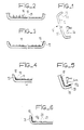
- the front panel 10 (FIG. 1) of a color television tube is constituted by a panel 11 on the internal face 12 of which the luminescent substances are deposited, as well as by a flange 13 intended to be connected to the conical part (not shown) of the tube.
- the glass 10 which is still bare, is first washed and dried of the panel 10. Then according to the invention, deionized water 14 (FIG. 1) is sprayed onto the face. internal 12a of rim 13.
- a solution of photosensitive material 15 (FIG. 2) is applied to the internal faces 12 and 12a.
- This photoresist 15 is then dried and then exposed, in a manner known per se, to ultraviolet (UV) light 16 at the locations where the phosphors will be deposited later.
- UV light 16 ultraviolet
- the parts 17 of the photoresist which have been exposed to ultraviolet radiation 16 are then hardened and insoluble in water.
- the jet of deionized water 14 makes it possible, relative to the prior art, to avoid the formation, in the film 18, of bubbles or cracks which are, after subsequent application of graphite, unsightly for the spectator.
- deionized water 14a (FIG. 5) is again sprayed onto the layer 19a of graphite covering the internal face of the rim or skirt 13.
Landscapes
- Physics & Mathematics (AREA)
- General Physics & Mathematics (AREA)
- Engineering & Computer Science (AREA)
- Manufacturing & Machinery (AREA)
- Formation Of Various Coating Films On Cathode Ray Tubes And Lamps (AREA)
- Vessels, Lead-In Wires, Accessory Apparatuses For Cathode-Ray Tubes (AREA)
- Cathode-Ray Tubes And Fluorescent Screens For Display (AREA)
Description
- L'invention est relative à un procédé de fabrication d'un tube de télévision en couleurs à faible réflectance de l'écran.
- L'écran d'un tube de télévision en couleurs est formé principalement de bandes verticales de luminophores destinés à émettre de la lumière de couleurs, respectivement rouge, verte et bleue, lorsqu'ils sont excités par des faisceaux d'électrons produits par les canons à l'intérieur du tube. Ces bandes luminescentes ne sont habituellement pas jointives ; elles sont séparées par des bandes neutres, c'est-à-dire dépourvues de luminophore. L'ensemble de ces bandes est recouvert d'une couche d'aluminium qui permet, notamment, de réfléchir vers l'avant, c'est-à-dire vers le spectateur, la lumière émise vers l'arrière par les luminophores. Mais cette couche d'aluminium constitue dans les zones neutres un miroir qui réfléchit la lumière ambiante et qui, ainsi altère la qualité - surtout lé contraste - de l'image. Pour remédier à cet inconvénient, on dépose, entre les bandes de luminophores, avant la formation de la couche d'aluminium, une couche noire antiréfléchissante, notamment en graphite. Cette opération de dépôt de couche noire, à laquelle se rapporte l'invention, est appelée « procédé Matrix » - voir, par exemple, EP-A-0 077 976.
- La couche noire antiréfléchissante- est également déposée sur la face interne du rebord, ou jupe, de la dalle (partie avant du tube sur laquelle est formé l'écran) qui raccorde cette dalle à la partie conique du tube. En effet, des reflets de la lumière ambiante sur ce rebord pourraient être gênants pour le spectateur surtout lorsque ce rebord est apparent, c'est-à-dire extérieur à l'ébénisterie du récepteur de télévision.
- On a constaté que le procédé connu de formation de la couche noire antiréfléchissante donnait parfois des résultats peu satisfaisants, le dépôt n'étant pas toujours régulier, pouvant même présenter des cloques ou craquelures. De plus, cette couche noire n'est pas suffisamment épaisse.
- L'invention perfectionne le procédé connu de façon à remédier à cet inconvénient. Elle fournit donc sur la face interne du rebord de la dalle une couche noire antiréfléchissante régulière et épaisse ; en outre le procédé selon l'invention est peu onéreux- et aisément utilisable pour une fabrication en grande série.
- Pour bien comprendre l'invention, avant d'exposer le perfectionnement, on rappelle tout d'abord comment est réalisé le procédé connu de formation des couches antiréfléchissantes.
- La face interne du panneau avant (dalle et son rebord) du tube est d'abord lavée et séchée.
- Puis, on applique sur cette face interne une substance photosensible appelée « photorésist » qui présente la propriété de durcir lorsqu'elle est illuminée par un rayonnement ultraviolet (UV) et, si elle n'a pas été illuminée, de pouvoir être éliminée par lavage à l'eau. La substance photosensible déposée est ensuite séchée, puis on expose aux rayonnements UV les zones de cette substance qui sont situées aux futurs emplacements des bandes luminescentes ; on procède ensuite au développement à l'eau. Il ne reste alors sur la face interne de la dalle que des bandes durcies aux emplacements où seront déposées ultérieurement les bandes de phosphores. Du graphite en suspension dans l'eau est ensuite appliqué sur la face interne du panneau avant. Ce graphite recouvre donc à la fois les bandes de matière photosensible durcie, le verre en principe à nu entre ces bandes, ainsi que le rebord.
- Après séchage, on projette une solution oxydante à base d'eau oxygénée H202 dont le but est d'attaquer chimiquement la substance photosensible durcie restant sur le verre, sous la couche de graphite. Enfin après un dernier développement, qui consiste à injecter de l'eau sous pression, le photorésist durci qui a été attaqué chimiquement par la solution oxydante se détache du verre, emmenant avec lui le graphite qui le recouvre. Il ne reste, alors, sur la dalle et sur le rebord que du graphite aux endroits voulus, c'est-à-dire aux emplacements entre les bandes de phosphores et sur rebord.
- L'invention repose sur l'hypothèse que la qualité médiocre du dépôt de graphite sur le rebord a l'origine suivante : lors de l'exposition au rayonnement ultraviolet, de la lumière diffusée atteint ce rebord, ce qui provoque la formation d'une mince couche, ou pellicule, de photorésist durci sur ce rebord. Cette pellicule n'est pas régulière et peut présenter des cloques, bulles ou craquelures, inesthétiques pour le spectateur après dépôt du graphite. Enfin lors de la dernière opération de développement, la solution oxydante attaque cette pellicule, ce qui altère la couche de graphite qui la recouvre.
- Pour remédier à cet inconvénient, c'est-à-dire pour obtenir une couche de graphite d'excellente qualité sur le rebord, l'invention telle qu'elle est caractérisée dans la revendication 1 prévoit des moyens pour rendre uniforme, et de préférence plus fine, la pellicule de substance photosensible durcie sur le rebord et/ou des moyens, déposés après l'application du graphite, qui permettent de réduire, ou annuler, l'effet de la solution oxydante sur la pellicule de substance photosensible durcie restant sur le rebord.
- Dans une réalisation, avant l'application de la substance photosensible on projette de l'eau, de préférence déionisée, sur le rebord. On a constaté qu'avec cette disposition le photorésist adhère plus aisément au verre et on produit ainsi sur le rebord, après l'illumination UV, une pellicule de substance photosensible plus uniforme et peut être plus fine. Autrement dit, la pellicule de substance photosensible durcie ne présente pas de cloques ou craquelures comme c'est le cas avec le procédé de la technique antérieure.
- On peut également utiliser de l'eau, de préférence déionisée, projetée sur la couche de graphite séchée, avant l'application de la solution oxydante (par exemple à base d'eau oxygénée), afin de réduire l'activité de cette solution oxydante sur la pellicule de photorésist durcie déposée sur le rebord, sous le graphite.
- D'autres caractéristiques de l'invention apparaîtront avec la description de l'un des ses modes de réalisation, celle-ci étant effectuée en se référant aux dessins ci-annexés sur lesquels :
- la figure 1 illustre une étape du procédé selon l'invention.
- les figures 2 à 4 sont des schémas montrant d'autres étapes, classiques, du procédé de dépôt de graphite sur la face interne du panneau avant d'un tube de télévision en couleurs,
- la figure 5 montre une étape du procédé selon l'invention et
- la figure 6 est un schéma dudit panneau après la mise en oeuvre du procédé de l'invention.
- Le panneau avant 10 (figure 1) d'un tube de télévision en couleurs est constitué par une dalle 11 sur la face interne 12 de laquelle sont déposées les substances luminescentes, ainsi que par un rebord 13 destiné à être raccordé à la partie conique (non représentée) du tube.
- Pour la fabrication de l'écran, on procède d'abord au lavage et au séchage du verre, encore à nu, du panneau 10. Ensuite selon l'invention, on projette de l'eau déionisée 14 (figure 1) sur la face interne 12a du rebord 13.
- Après cette projection d'eau déionisée 14 sur la face interne du rebord 13 on applique une solution de matière photosensible 15 (figure 2) sur les faces internes 12 et 12a. Ce photorésist 15 est ensuite séché puis exposé, de façon en soi connue, à de la lumière ultraviolette (UV) 16 aux emplacements où seront déposés ultérieurement les luminophores. Les parties 17 du photorésist qui ont été exposées au rayonnement ultraviolet 16 sont alors durcies et insolubles dans l'eau.
- On procède ensuite au développement de la substance photosensible 15 qui consiste à projeter de l'eau sur les faces internes 12 et 12a. Il ne reste alors (figure 3) que les zones 17 qui ont été illuminées. Toutefois les inventeurs ont constaté qu'il subsiste, malgré tout, une mince couche ou pellicule 18 de matière photosensible durcie aux emplacements qui n'ont pas été illuminés volontairement, notamment sur la face interne 12a du rebord 13. Cette pellicule 18, plus mince que les bandes 17, est probablement due à une diffusion, presque inévitable, de lumière ultraviolette vers le rebord. Cependant avec le mouillage préalable de ladite face interne 12a du rebord 13 à l'aide d'eau déionisée 14 cette pellicule 18 est, par rapport à une pellicule obtenue sans projection préalable d'eau déionisée, plus uniforme et probablement plus mince.
- De plus, le jet d'eau déionisée 14 (figure 1) permet, par rapport à la technique antérieure, d'éviter la formation, dans la pellicule 18, de bulles ou craquelures qui sont, après application ultérieure de graphite, inesthétiques pour le spectateur.
- Après développement de la matière photosensible, on répand une suspension de graphite noir sur les surfaces 12 et 12a recouvertes des bandes 17 et de la pellicule 18.
- Cette suspension est ensuite séchée et on obtient un dépôt de graphite 19 (figure 4) sur la face interne du panneau 10, à la fois sur les bandes 17 et entre celles-ci.
- Après ce séchage, selon l'invention, on projette de nouveau de l'eau déionisée 14a (figure 5) sur la couche 19a de graphite recouvrant la face interne du rebord ou jupe 13.
- Ensuite une solution d'eau oxygénée H202 est appliquée sur les faces internes 12 et 12a pour détruire, par attaque chimique, les bandes 17 de substance photosensible. Après un développement qui consiste en un lavage à l'eau sous pression, ces bandes 17 sont entraînées par le jet d'eau et entraînent avec elles le graphite qui les recouvre. Il ne reste ainsi sur la dalle que les bandes de graphite 20 (figure 6) déposées entre les bandes 17, c'est-à-dire entre les emplacements 21 où seront déposés ultérieurement les phosphores. La couche 19a de graphite sur le rebord 13 reste de bonne qualité grâce à la projection d'eau déionisée 14a qui a permis, par dilution et par refroidissement, de réduire l'activité chimique de l'eau oxygénée sur la pellicule sousjacente 18 de photorésist.
Claims (4)
Priority Applications (1)
| Application Number | Priority Date | Filing Date | Title |
|---|---|---|---|
| AT84401209T ATE31591T1 (de) | 1983-06-24 | 1984-06-13 | Verfahren zur herstellung von farbfernsehroehren mit geringer schirmzurueckstrahlung des umgebungslichtes. |
Applications Claiming Priority (2)
| Application Number | Priority Date | Filing Date | Title |
|---|---|---|---|
| FR8310498 | 1983-06-24 | ||
| FR8310498A FR2547950B1 (fr) | 1983-06-24 | 1983-06-24 | Procede de fabrication d'un tube de television en couleurs a faible reflectance de l'ecran pour la lumiere ambiante et tube obtenu par ce procede |
Publications (2)
| Publication Number | Publication Date |
|---|---|
| EP0130871A1 EP0130871A1 (fr) | 1985-01-09 |
| EP0130871B1 true EP0130871B1 (fr) | 1987-12-23 |
Family
ID=9290153
Family Applications (1)
| Application Number | Title | Priority Date | Filing Date |
|---|---|---|---|
| EP84401209A Expired EP0130871B1 (fr) | 1983-06-24 | 1984-06-13 | Procédé de fabrication d'un tube de télévision en couleurs à faible réflectance de l'écran pour la lumière ambiante |
Country Status (6)
| Country | Link |
|---|---|
| US (1) | US4533610A (fr) |
| EP (1) | EP0130871B1 (fr) |
| JP (1) | JPS6014729A (fr) |
| AT (1) | ATE31591T1 (fr) |
| DE (1) | DE3468291D1 (fr) |
| FR (1) | FR2547950B1 (fr) |
Families Citing this family (1)
| Publication number | Priority date | Publication date | Assignee | Title |
|---|---|---|---|---|
| WO2018221348A1 (fr) | 2017-05-30 | 2018-12-06 | デンカ株式会社 | Fibre de cheveux artificiels |
Family Cites Families (12)
| Publication number | Priority date | Publication date | Assignee | Title |
|---|---|---|---|---|
| GB1243663A (en) * | 1968-02-02 | 1971-08-25 | Kodak Ltd | Manufacture of coated layers |
| US3712815A (en) * | 1970-06-30 | 1973-01-23 | Westinghouse Electric Corp | Method of manufacturing a display screen |
| US3788846A (en) * | 1971-06-28 | 1974-01-29 | Rca Corp | Method for printing negative tolerance matrix screen structure for a cathode-ray tube |
| JPS4924573A (fr) * | 1972-06-30 | 1974-03-05 | ||
| JPS5144473A (ja) * | 1974-10-14 | 1976-04-16 | Hitachi Ltd | Buratsukumatoritsukusutaipuno karaajuzokanyokeikomenno seizohoho |
| US3998638A (en) * | 1975-05-22 | 1976-12-21 | Westinghouse Electric Corporation | Method of developing opaquely coated sensitized matrix with a solution containing sodium meta-silicate |
| JPS5922340B2 (ja) * | 1975-06-04 | 1984-05-25 | 株式会社日立製作所 | カラ−受像管けい光面製造方法 |
| JPS5546410A (en) * | 1978-09-29 | 1980-04-01 | Hitachi Ltd | Constructing method of fluorescent screen for color picture tube |
| US4234669A (en) * | 1979-03-27 | 1980-11-18 | Rca Corporation | CRT Screen structure produced by photographic method |
| JPS56132742A (en) * | 1980-03-19 | 1981-10-17 | Toshiba Corp | Formation of phosphor surface for color-picture tube |
| JPS56132741A (en) * | 1980-03-19 | 1981-10-17 | Hitachi Ltd | Formation of phosphor surface for color-picture tube |
| DE3142261A1 (de) * | 1981-10-24 | 1983-05-05 | Standard Elektrik Lorenz Ag, 7000 Stuttgart | Verfahren zur erzeugung einer schwarzmatrixschicht zwischen den leuchtflaechen auf der innenseite der wannen von farbbildroehren |
-
1983
- 1983-06-24 FR FR8310498A patent/FR2547950B1/fr not_active Expired
-
1984
- 1984-06-13 DE DE8484401209T patent/DE3468291D1/de not_active Expired
- 1984-06-13 AT AT84401209T patent/ATE31591T1/de not_active IP Right Cessation
- 1984-06-13 EP EP84401209A patent/EP0130871B1/fr not_active Expired
- 1984-06-21 US US06/622,824 patent/US4533610A/en not_active Expired - Lifetime
- 1984-06-22 JP JP59129033A patent/JPS6014729A/ja active Pending
Also Published As
| Publication number | Publication date |
|---|---|
| FR2547950B1 (fr) | 1986-01-31 |
| DE3468291D1 (en) | 1988-02-04 |
| EP0130871A1 (fr) | 1985-01-09 |
| FR2547950A1 (fr) | 1984-12-28 |
| US4533610A (en) | 1985-08-06 |
| JPS6014729A (ja) | 1985-01-25 |
| ATE31591T1 (de) | 1988-01-15 |
Similar Documents
| Publication | Publication Date | Title |
|---|---|---|
| FR2751127A1 (fr) | Procede de formation de nervures de barrage, et panneau d'affichage a decharge dans un plasma | |
| KR950000345B1 (ko) | 음극선관 | |
| EP0313448B1 (fr) | Procédé de métallisation d'un écran luminescent | |
| EP0130871A1 (fr) | Procédé de fabrication d'un tube de télévision en couleurs à faible réflectance de l'écran pour la lumière ambiante | |
| JPH07201287A (ja) | カラー陰極線管の蛍光面及びその製造方法 | |
| US5547411A (en) | Method of manufacturing color cathode ray tube screen | |
| FR2569048A1 (fr) | Procede de fabrication d'un ecran luminescent pour un tube image en couleurs | |
| JPH11339683A (ja) | 陰極線管およびその製造方法 | |
| US5723170A (en) | Method of forming fluorescent screen of cathode ray tube | |
| US4369241A (en) | Method of forming a fluorescent screen of a black matrix type color picture tube | |
| US4855200A (en) | Fluorescent screens of color picture tubes and manufacturing method therefor | |
| GB2221087A (en) | Method of manufacturing phosphor screens for cathode ray tubes | |
| JPH047055B2 (fr) | ||
| FR2758206A1 (fr) | Procede de fabrication d'une cathode a emission de champ | |
| JP3483577B2 (ja) | フラットパネルディスプレー構造における平面アルミニウム層の製造法 | |
| FR2747838A1 (fr) | Composition formant un film fluorescent destine a un affichage et procede de formation d'un film fluorescent destine a un affichage | |
| JPH08298073A (ja) | カラー陰極線管蛍光面の製造方法 | |
| JPS59937B2 (ja) | カラ−受像管けい光面製造方法 | |
| KR20010065042A (ko) | 칼라 브라운관의 형광면 및 그의 제조 방법 | |
| JPH02247954A (ja) | 陰極線管螢光面用フィルミング材料 | |
| JPH11162346A (ja) | 蛍光面におけるブラックストライプの形成方法 | |
| JP2517007B2 (ja) | カラ―受像管用蛍光面 | |
| FR2797991A1 (fr) | Panneau d'affichage au plasma a contraste et colorimetrie ameliorees et procede fabrication d'un tel panneau | |
| JPS59219832A (ja) | カラ−受像管螢光面の形成方法 | |
| JPS6232570B2 (fr) |
Legal Events
| Date | Code | Title | Description |
|---|---|---|---|
| PUAI | Public reference made under article 153(3) epc to a published international application that has entered the european phase |
Free format text: ORIGINAL CODE: 0009012 |
|
| AK | Designated contracting states |
Designated state(s): AT DE FR GB IT NL |
|
| 17P | Request for examination filed |
Effective date: 19850131 |
|
| GRAA | (expected) grant |
Free format text: ORIGINAL CODE: 0009210 |
|
| AK | Designated contracting states |
Kind code of ref document: B1 Designated state(s): AT DE FR GB IT NL |
|
| REF | Corresponds to: |
Ref document number: 31591 Country of ref document: AT Date of ref document: 19880115 Kind code of ref document: T |
|
| ITF | It: translation for a ep patent filed | ||
| REF | Corresponds to: |
Ref document number: 3468291 Country of ref document: DE Date of ref document: 19880204 |
|
| GBT | Gb: translation of ep patent filed (gb section 77(6)(a)/1977) | ||
| PLBE | No opposition filed within time limit |
Free format text: ORIGINAL CODE: 0009261 |
|
| STAA | Information on the status of an ep patent application or granted ep patent |
Free format text: STATUS: NO OPPOSITION FILED WITHIN TIME LIMIT |
|
| 26N | No opposition filed | ||
| PG25 | Lapsed in a contracting state [announced via postgrant information from national office to epo] |
Ref country code: AT Effective date: 19890613 |
|
| ITTA | It: last paid annual fee | ||
| PGFP | Annual fee paid to national office [announced via postgrant information from national office to epo] |
Ref country code: GB Payment date: 19980429 Year of fee payment: 15 |
|
| PGFP | Annual fee paid to national office [announced via postgrant information from national office to epo] |
Ref country code: DE Payment date: 19980615 Year of fee payment: 15 |
|
| PGFP | Annual fee paid to national office [announced via postgrant information from national office to epo] |
Ref country code: NL Payment date: 19980630 Year of fee payment: 15 |
|
| PG25 | Lapsed in a contracting state [announced via postgrant information from national office to epo] |
Ref country code: GB Free format text: LAPSE BECAUSE OF NON-PAYMENT OF DUE FEES Effective date: 19990613 |
|
| PGFP | Annual fee paid to national office [announced via postgrant information from national office to epo] |
Ref country code: FR Payment date: 19990927 Year of fee payment: 16 |
|
| PG25 | Lapsed in a contracting state [announced via postgrant information from national office to epo] |
Ref country code: NL Free format text: LAPSE BECAUSE OF NON-PAYMENT OF DUE FEES Effective date: 20000101 |
|
| GBPC | Gb: european patent ceased through non-payment of renewal fee |
Effective date: 19990613 |
|
| NLV4 | Nl: lapsed or anulled due to non-payment of the annual fee |
Effective date: 20000101 |
|
| PG25 | Lapsed in a contracting state [announced via postgrant information from national office to epo] |
Ref country code: DE Free format text: LAPSE BECAUSE OF NON-PAYMENT OF DUE FEES Effective date: 20000503 |
|
| PG25 | Lapsed in a contracting state [announced via postgrant information from national office to epo] |
Ref country code: FR Free format text: LAPSE BECAUSE OF NON-PAYMENT OF DUE FEES Effective date: 20010228 |
|
| REG | Reference to a national code |
Ref country code: FR Ref legal event code: ST |